Wide Dynamic Range CMOS Potentiostat for Amperometric Chemical Sensor

Abstract
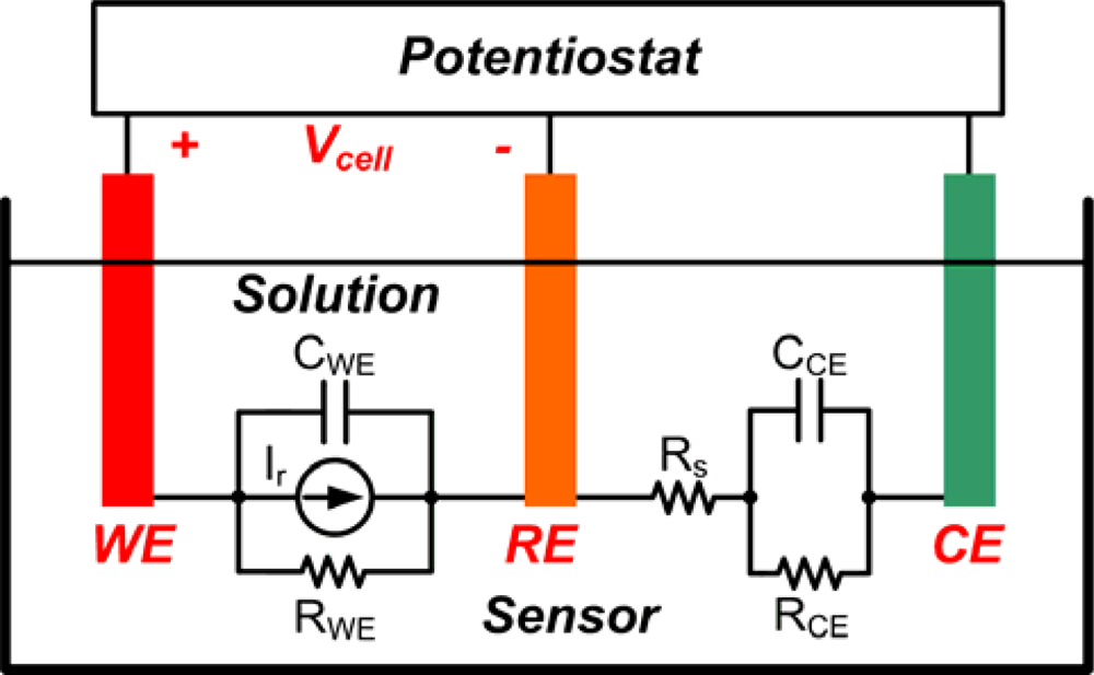
:1. Introduction
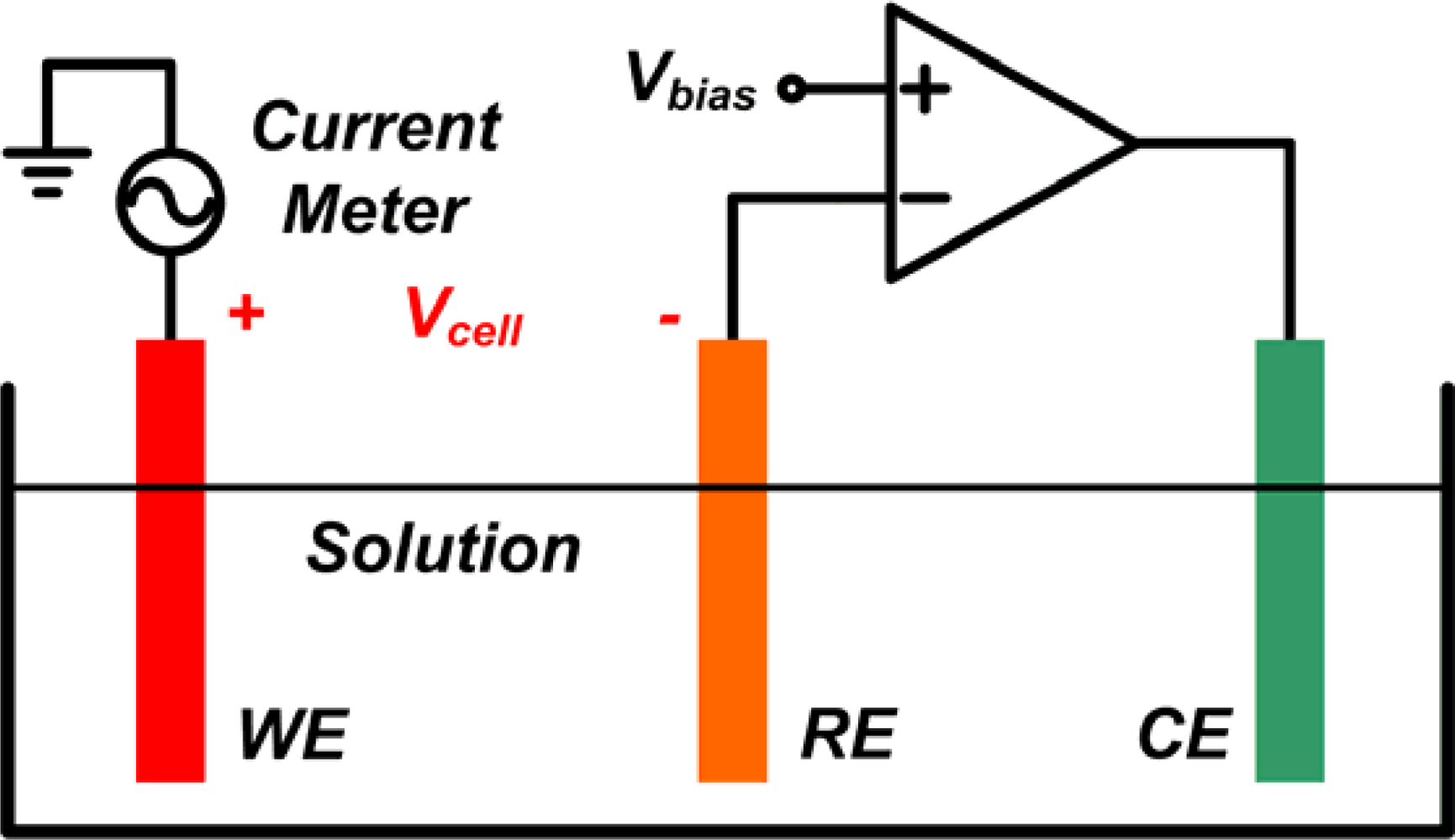
1.1. Potential Control Configuration
1.2. Current Measurement Configuration
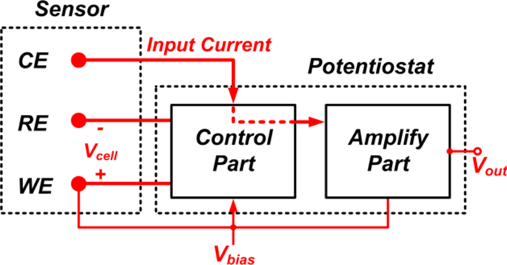
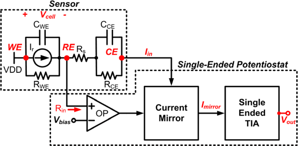
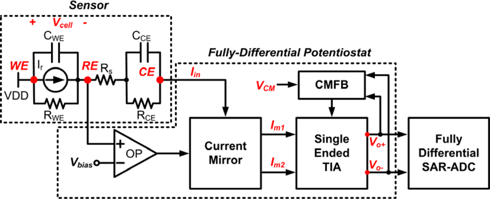
2. Proposed Potentiostat Topology
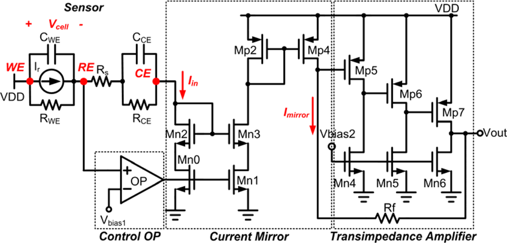
2.1. Single-ended Potentiostat
a) Control Part
b) Amplifying Part
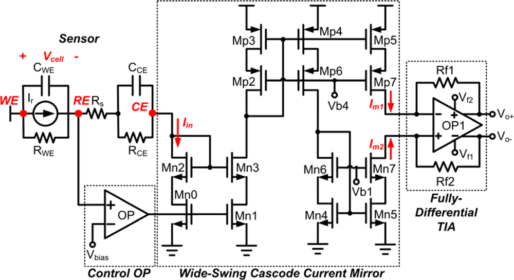
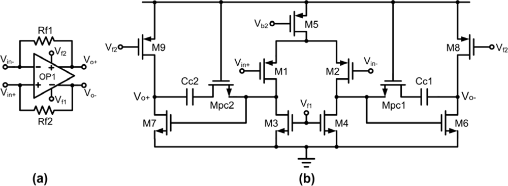
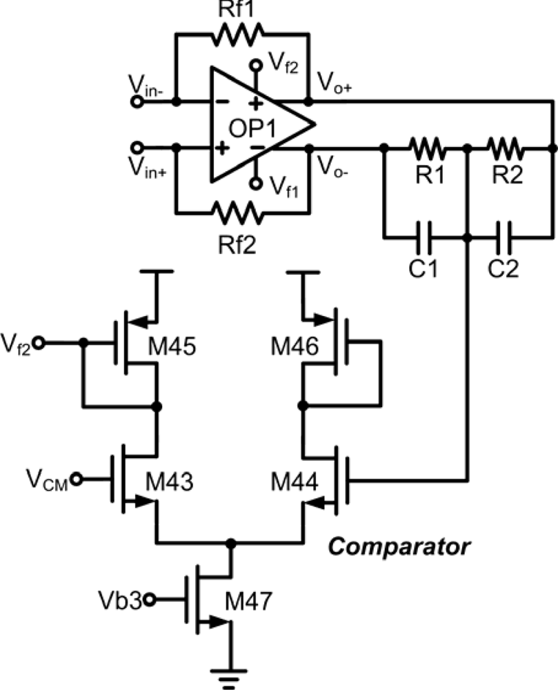
2.2. Fully-differential Potentiostat
a) Wide-Swing Cascode Current Mirror
b) Fully-differential Transimpedance Amplifier
3. Measurement Results and Discussion
3.1. Measurement Results for Single-ended Potentiostat
3.2. Measurement Results for Fully-differential Potentiostat
4. Conclusions
Acknowledgments
References
- Busoni, L.; Carla, M.; Lanzi, L. A comparison between potentiostatic circuits with grounded work or auxiliary electrode. Rev. Scient. Instrum 2002, 73, 1921–1923. [Google Scholar]
- Fidler, J.C.; Penrose, W.R.; Bobis, J.P. A potentiostat based on a voltage-controlled current source for use with amperometric gas sensors. IEEE Trans. Instrum. Measure 1992, 41, 308–310. [Google Scholar]
- Chung, W.Y.; Paglinawan, A.C.; Wang, Y.-H.; Kuo, T.T. A 600 μm read-out circuit with potentiostat for amperometric chemical sensors and glucose meter applications. Proceedings of IEEE Conference on Electron Devices and Solid-State Circuits, Tainan, Taiwan, December 20–22, 2007; pp. 1087–1090.
- Jichun, Z.; Trombly, N.; Mason, A. A low noise readout circuit for integrated electrochemical biosensor arrays. Processing of IEEE Sensors, Vienna, Austria, October 24–27, 2004; pp. 36–39.
- Reay, R.J.; Kounaves, S.P.; Kovacs, G.T.A. An integrated CMOS potentiostat for miniaturized electroanalytical instrumentation. Proceedings of IEEE International Solid-State Circuits Conference, San Francisco, CA, USA, February 24–27, 1994; pp. 162–163.
- Iniewski, K. VLSI Circuits for Biomedical Applications, 1st ed; Artech House: Boston, MA, USA, 2008; pp. 272–275. [Google Scholar]
- Genov, R.; Stanacevic, M.; Naware, M.; Cauwenberghs, G.; Thakor, N.V. 16-channel integrated potentiostat for distributed neurochemical sensing. IEEE Trans. Circ. Syst. I: Regular Papers 2006, 53, 2371–2376. [Google Scholar]
- Ayers, S.; Gillis, K.D.; Lindau, M.; Minch, B.A. Design of a CMOS potentiostat circuit for electrochemical detector arrays. IEEE Trans. Circ. Syst. I: Regular Papers 2007, 54, 736–744. [Google Scholar]
- Hasan, S.M.R. Stability analysis and novel compensation of a CMOS current-feedback potentiostat circuit for electrochemical sensors. IEEE Sens. J 2007, 7, 814–824. [Google Scholar]
- Narula, H.S.; Harris, J.G. A time-based VLSI potentiostat for ion current measurements. IEEE Sens. J 2006, 6, 239–247. [Google Scholar]
- Turner, R.F.B.; Harrison, D.J.; Baltes, H.P. A CMOS potentiostat for amperometric chemical sensors. IEEE J. Solid-State Circuits 1987, 22, 473–478. [Google Scholar]
- Narula, H.S.; Harris, J.G. Integrated VLSI potentiostat for cyclic voltammetry in electrolytic reactions. Proceedings of IEEE Computer Society Annual Symposium on VLSI, Lafayette, LA, USA, February 19–20, 2004; pp. 268–270.
- Stanacevic, M.; Murari, K.; Rege, A.; Cauwenberghs, G.; Thakor, N.V. VLSI potentiostat array with oversampling gain modulation for wide-range neurotransmitter sensing. IEEE Trans. Biomed. Circ. Syst 2007, 1, 63–72. [Google Scholar]
- Ahmadi, M.M.; Jullien, G.A. A very low power CMOS potentiostat for bioimplantable applications. Proceedings of Fifth International Workshop on System-on-Chip for Real-Time Applications, Banff, Alberta, Canada, July 20–24, 2004; pp. 184–189.
- Sauerbrey, J.; Schmitt-Landsiedel, D.; Thewes, R. A 0.5-V 1-uW successive approximation ADC. IEEE J. Solid-State Circuits 2003, 38, 1261–1265. [Google Scholar]
- Kakerow, R.G.; Kappert, H.; Spiegel, E.; Manoli, Y. Low-power single-chip CMOS potentiostat. Proceedings of the 8th International Conference on Solid-State Sensors and Actuators, Stockholm, Sweden, June 25–29, 1995; pp. 142–145.
- Martin, S.M.; Gebara, F.H.; Strong, T.D.; Brown, R.B. A fully differential potentiostat. IEEE Sens. J 2009, 9, 135–142. [Google Scholar]
- Ahmadi, M.M.; Jullien, G.A. Current-mirror-based potentiostats for three-electrode amperometric electrochemical sensors. IEEE Trans. Circ. Syst. I: Regular Papers 2009, 56, 1339–1348. [Google Scholar]


| IEEE IWSOC’05 [14] | IEEE ICSSA’95[16] | IEEE Sensors J.’09 [17] | IEEE ITCAS’09 [18] | This Work (SE) | This Work (FD) | |
|---|---|---|---|---|---|---|
| Year | 2005 | 1995 | 2009 | 2009 | 2009 | 2009 |
| Power Supply (V) | 1.8 | 5 | ± 0.9V | 1.8 | 1.8 | 1.8 |
| Process (um) | 0.18 | 1 | 0.18 | 0.18 | 0.18 | 0.18 |
| Irange (A) | 1 n∼200 n | 0.1 n∼0.5 u | X | 1 n∼1 u | 10 n∼10 u | 500 p ∼ 10 u |
| Dynamic Range (dB) | 46.02 | 73.98 | 63 | 60 | 60 | 86 |
| Ireadout Electrode | CE | WE | WE | CE | CE | CE |
| Control Part | SE | SE | FD | SE | SE | SE |
| Readout Circuit | SE | SE | FD | SE | SE | FD |
| Output Signal | Freq. | VDT | VCT | Freq. | VCT | VCT |
| Core Area (mm2) | 0.04 | 0.6 | 0.45 | 0.02 | 0.013 | 0.066 |
© 2010 by the authors; licensee Molecular Diversity Preservation International, Basel, Switzerland. This article is an open access article distributed under the terms and conditions of the Creative Commons Attribution license (http://creativecommons.org/licenses/by/3.0/).
Share and Cite
Wang, W.-S.; Kuo, W.-T.; Huang, H.-Y.; Luo, C.-H. Wide Dynamic Range CMOS Potentiostat for Amperometric Chemical Sensor. Sensors 2010, 10, 1782-1797. https://doi.org/10.3390/s100301782
Wang W-S, Kuo W-T, Huang H-Y, Luo C-H. Wide Dynamic Range CMOS Potentiostat for Amperometric Chemical Sensor. Sensors. 2010; 10(3):1782-1797. https://doi.org/10.3390/s100301782
Chicago/Turabian StyleWang, Wei-Song, Wei-Ting Kuo, Hong-Yi Huang, and Ching-Hsing Luo. 2010. "Wide Dynamic Range CMOS Potentiostat for Amperometric Chemical Sensor" Sensors 10, no. 3: 1782-1797. https://doi.org/10.3390/s100301782