Article

An Analog Multilayer Perceptron Neural Network for a Portable Electronic Nose

Department of Electrical Engineering, National Tsing Hua University, No. 101, Sec. 2, Kuang-Fu Road, 30013 Hsinchu, Taiwan
*
Author to whom correspondence should be addressed.
Sensors 2013, 13(1), 193-207; https://doi.org/10.3390/s130100193
Submission received: 10 November 2012 / Revised: 17 December 2012 / Accepted: 19 December 2012 / Published: 24 December 2012

Abstract

:
This study examines an analog circuit comprising a multilayer perceptron neural network (MLPNN). This study proposes a low-power and small-area analog MLP circuit to implement in an E-nose as a classifier, such that the E-nose would be relatively small, power-efficient, and portable. The analog MLP circuit had only four input neurons, four hidden neurons, and one output neuron. The circuit was designed and fabricated using a 0.18 μm standard CMOS process with a 1.8 V supply. The power consumption was 0.553 mW, and the area was approximately 1.36 × 1.36 mm2. The chip measurements showed that this MLPNN successfully identified the fruit odors of bananas, lemons, and lychees with 91.7% accuracy.

1. Introduction

The artificial olfactory system, also referred to as the electronic nose (E-nose) system, has been used in numerous applications. These include air quality monitoring, food quality control [1], hazardous gas detection, medical treatment and health care [2], and diagnostics [3]. An E-nose system comprises a sensor array, a signal processing unit, and a pattern recognition system. During recent decades a substantial amount of research and development has been reported on E-nose systems. Because of the complex classification algorithms embedded in the pattern recognition system, a central processing unit (CPU) is usually required [1,2]. Consequently, the majority of E-nose systems is large and consumes considerable power. However, heavy and power-hungry equipment is inconvenient to use, and designing a low-power small device would be preferable. Some researchers and companies [46] have used microprocessors or field-programmable gate arrays (FPGAs) as a computational cell to develop portable E-noses, but these systems are still too power-intensive and large. To further reduce the power consumption and device area, analog VLSI implementation of the learning algorithm for E-nose application has been proposed [714].
The multilayer perceptron neural network (MLPNN) is an algorithm that has been continuously developed for many years. Consequently, when VLSI implementation of a learning algorithm is necessary, MLPNN is a common choice. In 1986, Hopfield and Tank proposed the first analog MLPNN circuit [10]. Since then, several analog VLSI implementations of MLPNN have been proposed [1114]. Some have focused on the improvement of the multiplier [1418] and some have attempted to design a nonlinear synapse to remove the analog multiplier [19,20]. However, the power consumption for most of the MLPNN circuits range from a few milliwatts to a few hundred milliwatts [1114]. This power consumption is still too high for portable applications. Consequently, an MLPNN circuit with considerably lower power consumption (lower than 1 mW) is required when an MLPNN is being implemented in a portable E-nose.
This study implemented a low power MLPNN by analog VLSI circuit to serve as a classification unit in an E-nose. Neural networks is one of the most popular algorithms used in an E-nose system [2,5], because it can recognize and identify odor signal patterns. A typical MLPNN contains one input layer; one or more hidden layer(s), depending on the application; and an output layer. Apart from the input layer, both the hidden and output layers contain several neurons with nonlinear activation functions, which constitute the signal processing unit. Synapses connect the neurons of different layers, and a weight unit is included in each synapse. The weight units and the outputs of neurons determine the input of neurons in subsequent layers. An analog circuit realizes a nonlinear function with a simple structure [15]. Thus, implementing an analog MLPNN circuit reduces the need for power and the size of the pattern recognition unit required to build an E-nose.
The weight adaptation algorithm used in this study was the back propagation (BP) learning algorithm [21]. This algorithm allows the weights to be adjusted so that the MLP network can learn the target function; that is, pattern recognition. The details of the MLPNN and BP algorithms are provided below.
The input of a neuron can be represented as:
a j H = i = 1 n I W j i H X i I
where ajH is the input of the jth hidden neuron; WjiH represents the weight of the synapse that connects the jth hidden neuron and the ith input neuron; XiI represents the output of the ith input neuron; and nI is the number of input neurons. Neuron output is determined by its input and activation function. The hyper tangent function is one of the most commonly used activation functions. This function can be easily implemented by analog VLSI with small chip area and power consumption. Consequently, the hyper tangent activation was chosen for this work. By choosing hyper tangent activation function, the neuron output is:
X j H = tan h ( a j H ) + b j
where XjH is the output of the jth hidden neuron, and bj represents the bias value.
Similar to the hidden neuron, the input of the kth output neuron is:
a k O = j = 1 n H W k j O X j H
The output of the kth output neuron XkO is:
X k O = tan h ( a k O ) + c k
where ck represents the bias value.
After calculating the output XkO of the output neuron, we derived the adapting value by comparing the circuit output XkO with target output Xt.
According to the BP algorithm, the general weight update value ΔW is derived by:
Δ W = η E p a a W
where a represents the neuron input; η is the learning rate, and Ep is the error term derived from the comparison between circuit output XkO and target Xt. In the following content, we used the mean square error and assumed that there was a single output neuron. Consequently, XkO was simplified to XO.
The order of weight adaptation proceeds from the output layer to the input layer. When deriving ΔW in each layer, repeatedly differentiating the error by weight is unnecessary because certain computations have already been performed in later layers (for the hidden layer, the later layer is the output layer). The later layer propagates the computation to the previous layer; this propagating value is called the “back propagation error.” For the output layer, the BP error δO is:
δ O = E p a O = ( X t X O ) × D O
where DO represents the differentiation of the output neuron's activation function. For the hidden layer, the BP error of the jth hidden neuron δ j H is:
δ j H = E p a j H = δ O × W j O × D j H
From Equations (1), (3), (5), (6) and (7), ΔWjO and ΔWjiH are derived as Equations (8) and (9), respectively:
Δ W j O = η × ( X t X O ) × D O × a O W j O = η ( X t X O ) × D O × X j H
Δ W j i H = η × ( δ O × W j O × D j H ) × a j H W j i H = η × ( δ O × W j O × D j H ) × X i I
The MLPNN was trained by adapting the weights according to Equation (10). During the training phase, the new weight Wnew in a synapse was acquired from the previous weight Wold in the same synapse plus the weight update value ΔW:
W new = W old + Δ W
The rest of this paper is organized as follows: Section 2 describes the system architecture, Section 3 presents the measurement results, and Section 4 presents the conclusion.

2. Architecture and Implementation

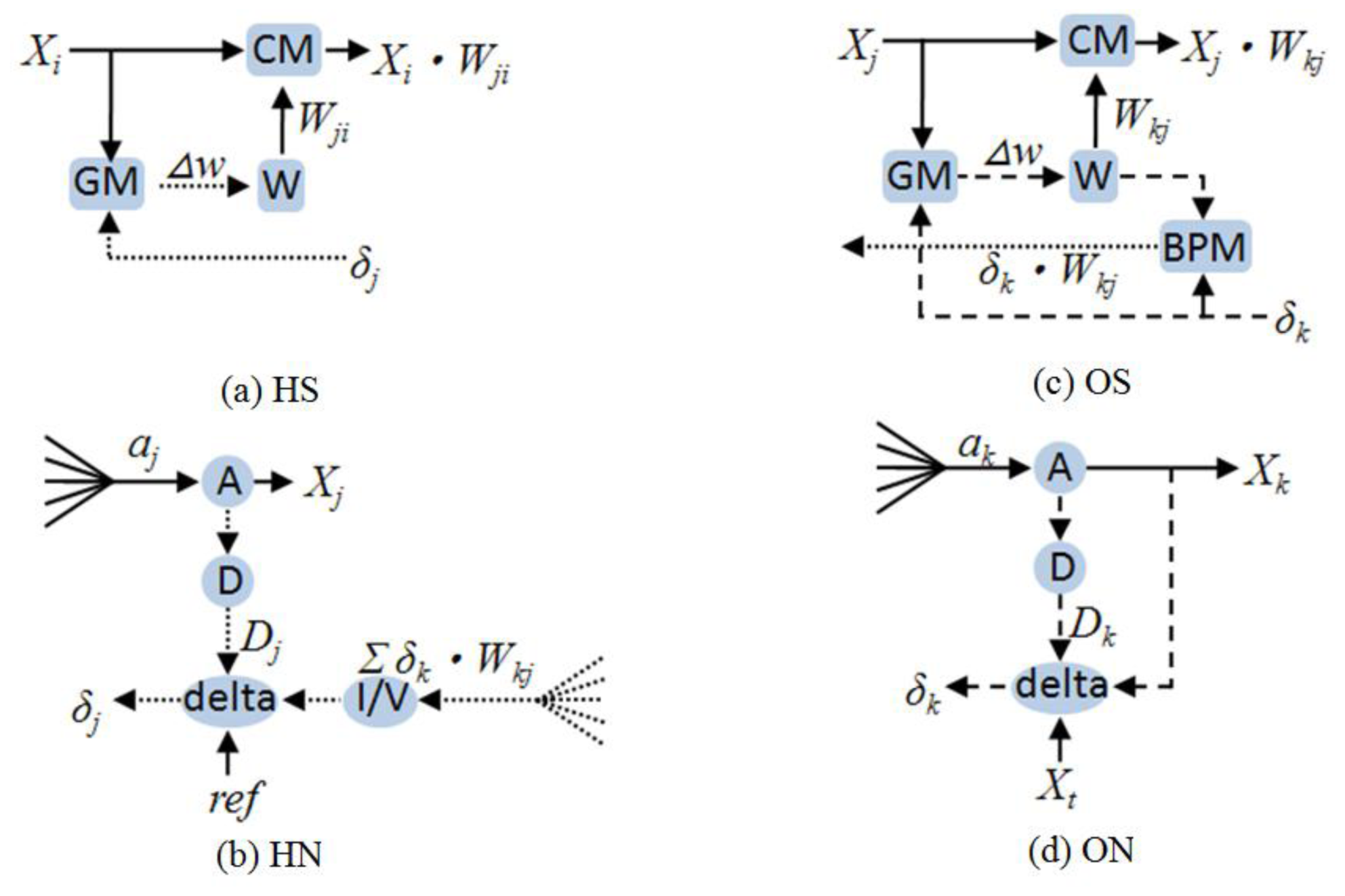
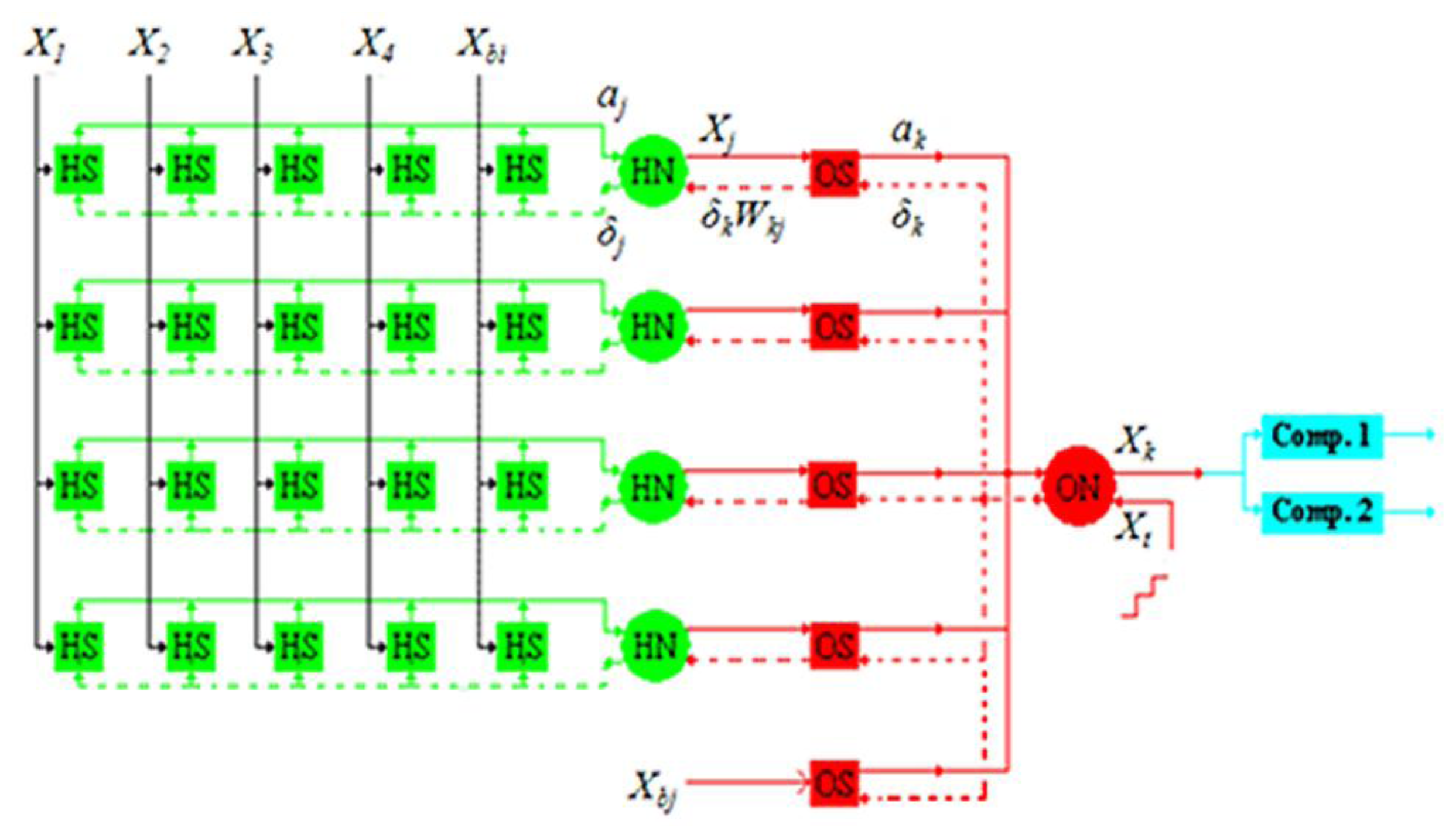
This paper proposes a 4-4-1 MLPNN. The 4-4-1 notation represents four input neurons, four hidden neurons, and one output neuron. This structure was proven by Matlab to be able to learn the odor data we used before really doing chip design. The block diagram is shown in Figure 1. The symbols X1X4 refer to four signal inputs; Xbi is the bias in the input layer; HSs are the synapses between the input and hidden layers; HNs are the hidden neurons; Xbj is the bias in the hidden layer; OSs are the synapses between the hidden and output layers; and ON is the output neuron.
Based on Equations (1) to (10), the detailed block diagram of HS, HN, OS, and ON was obtained, as shown in Figure 2. The CM, BPM and GM are multipliers; W is weight; A is the activation function; D is the differentiation of activation function; delta is the BP error generator; and I/V is the current-to-voltage converter.
Because several multiplication results are summed in Equations (1) and (3), the output signals of all multipliers are designed as current signals. Using Kirchhoff's current laws (KCL), the current is summed if the outputs of the synapses are connected. Thus, the area and power of the system are reduced because no extra analog adder is necessary. For signals that require transmission to several nodes (e.g., X1 to X4), a voltage signal is preferred. Further description of the subblocks shown in Figure 2 and the relations between the equations and sub-blocks are provided below. When approximating the equations by analog circuit, second-order effects, such as the body or Early effect, are neglected; thus, particular errors may be introduced. These errors may result in nonlinearity. However, by carefully designing the bias, size, and dynamic range of the circuit, the nonlinearity has little effect on the learning performance of the application in this study.

2.1. Synapses

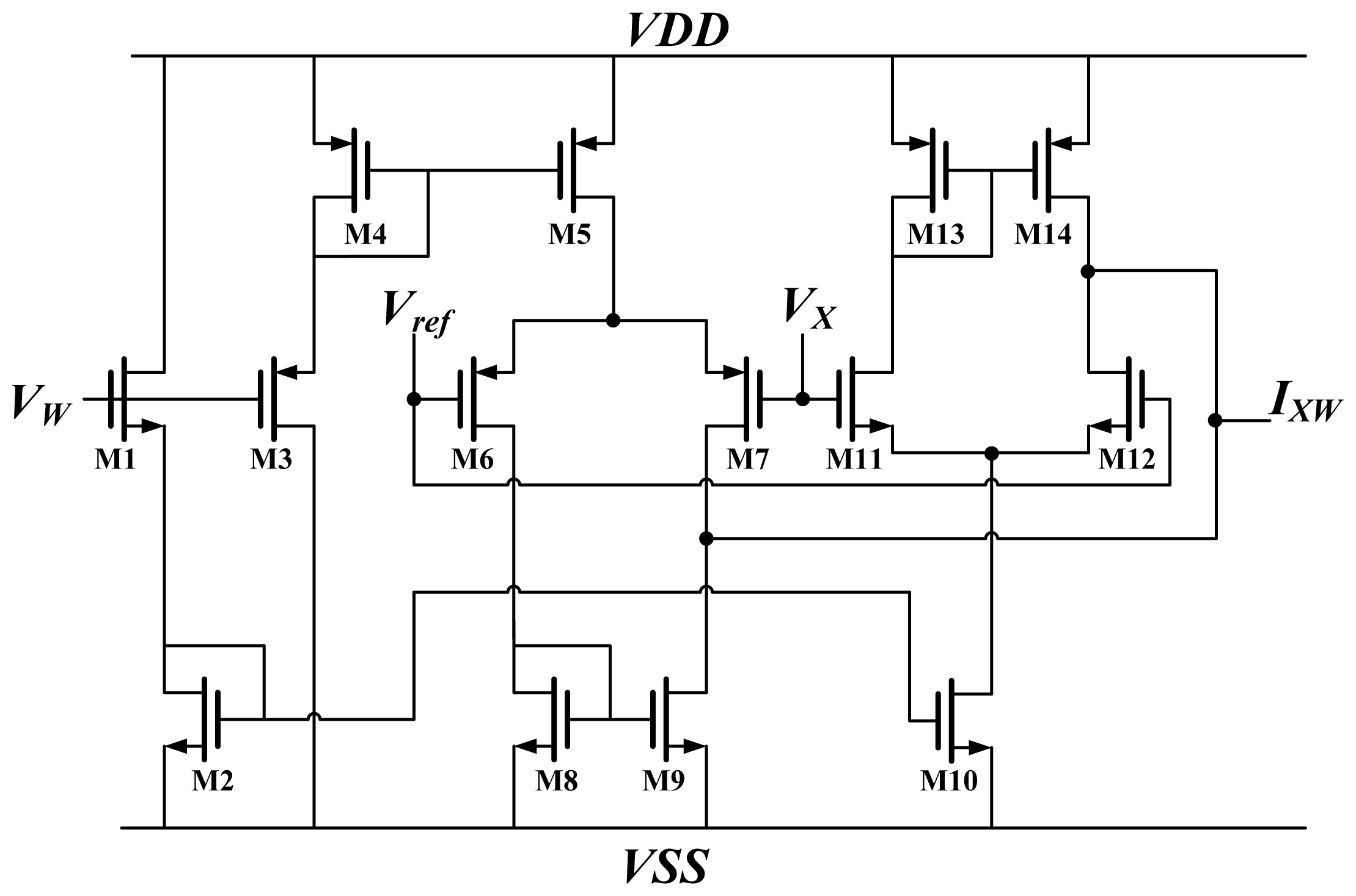
The synapses at the hidden layer and the output layer comprise two multipliers (CM and GM) and a weight unit W; the output layer synapse needs one more multiplier (BPM) to generate the term δOkkWjO. The terms BPM and CM are both Chible's multipliers [16,17]. The BPM multiplies the weight by BP error, whereas CM is used to multiply the input by weight. The results represent the current. This study used the Chible's multiplier because of its wide operation range [16]. A schematic diagram of Chible's multiplier is shown in Figure 3.
The weight and input are voltages, denoted by VW and VX, respectively. The output of the multiplier is IXW. M1, M3 operate in strong inversion regions, whereas M6, M7, M11, and M12 operate in weak inversion regions. According to the equation of MOSFET in strong and weak inversion, the output current is:
I W X = ( I w p I w n ) × tan h ( κ ( V x V ref ) 2 U T ) = I w × tan h ( κ V x ref 2 U T )
where Vref is a reference voltage; UT is thermal voltage; and Iwp and Iwn represent the bias current for M6 and M7 and for M11 and M12, respectively. Both Iwp and Iwn are related to weight VW. Assuming that the parameters for NMOS and PMOS are equal and Vx-ref is sufficiently small, IWX is equal to VW_offset multiplied by VX_offset. Furthermore, VW_offset and VX_offset represent VW and VX plus an offset, respectively.
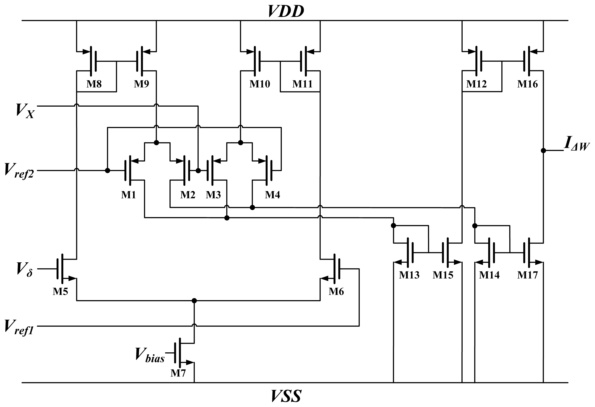
The GM term represents the Gilbert multiplier [22,23]. This type of multiplier provides good linearity but a small dynamic range. Thus, this block multiplies the neuron output X and error term δ in Equations (8) and (9). The schematic is shown in Figure 4. The output X and BP error δ are voltages, denoted by VX and Vδ, respectively. The output of the multiplier is IΔW, whereas Vref1 and Vref2 are reference voltages. All of the MOSFETs operate in subthreshold regions. According to the voltage and current relationship of MOSFETs in subthreshold regions, the output current is represented as:
I Δ W = I bias × tan h ( κ ( V x V ref 2 ) 2 U T ) × tan h ( κ ( V δ V ref 1 ) 2 U T )
when the difference of VX and Vδ to the reference voltage are sufficiently small, IΔW can be simplified to:
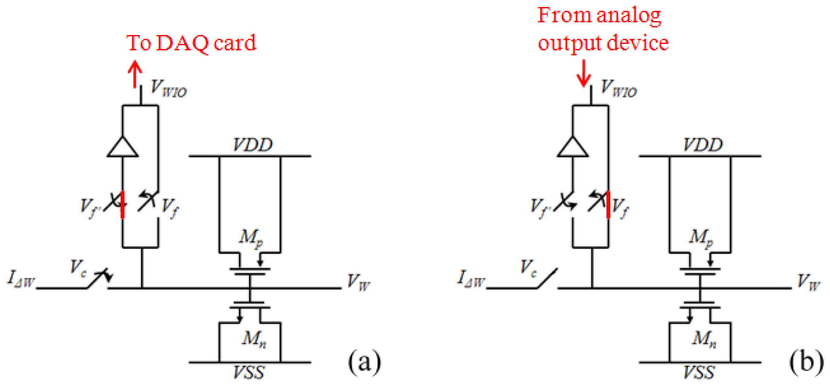
I Δ W = I bias × κ ( V x V ref 2 ) 2 U T × κ ( V δ V ref 1 ) 2 U T
The weight unit W is a temporal signal storage device showing the characteristic of Equation (10). The circuit implementation of the weight unit is shown 
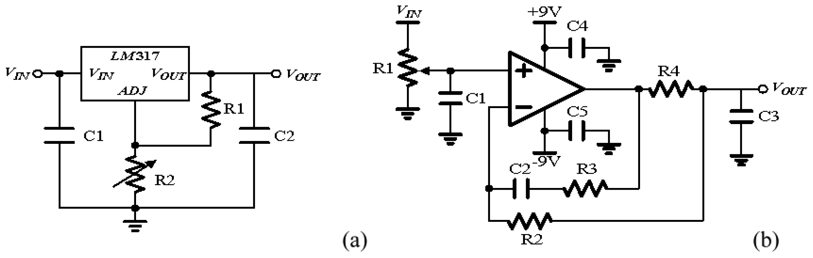
Figure 5. The weight is represented by a voltage that is stored on a capacitor. This study used metal-oxide semiconductors to form a MOSCap. Compared to other types of capacitors, the MOSCap has a larger capacitance per unit area. Thus, the chip area is reduced by using a MOSCap. In the training phase, the weight adaptation is performed using a weight-updating current IΔW from the 
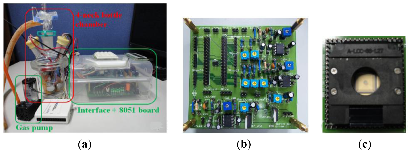
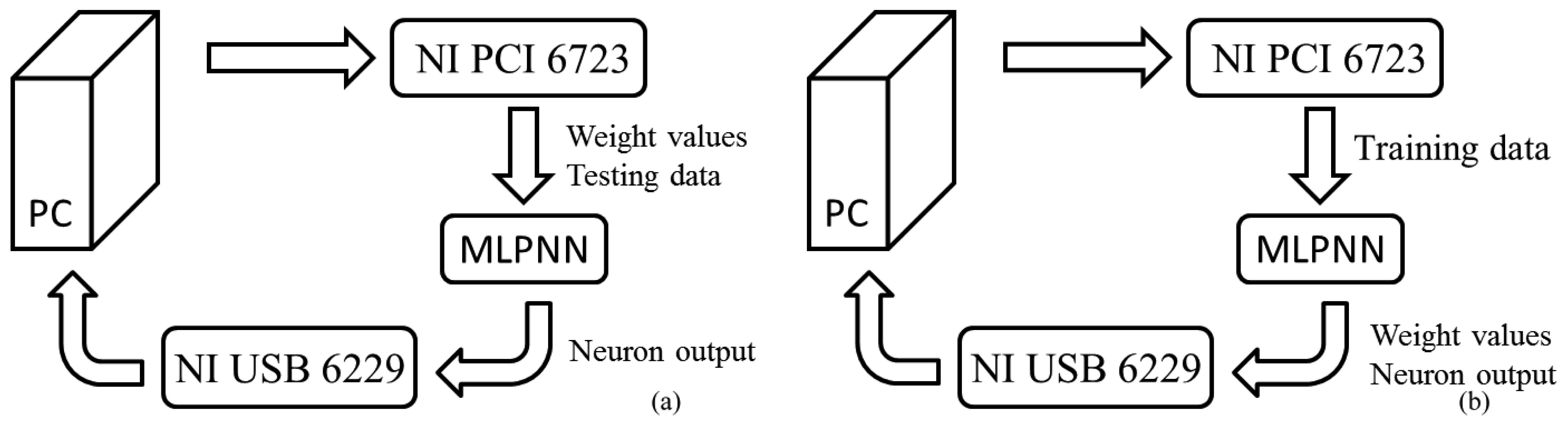
GM to charge or discharge the storage capacitor. The control voltage Vc determined the period for the current to charge or discharge the capacitor; in other words, this control voltage determines the learning rate of the network. The weight value is collected simultaneously by a data acquisition device (NI 6229). These weight values are stored in a computer. In the classifying phase, IΔW no longer updates the weight values; rather, the computer sets the weights on the MLPNN chip using pre-stored weight values through a data application device (NI PCI 6723).
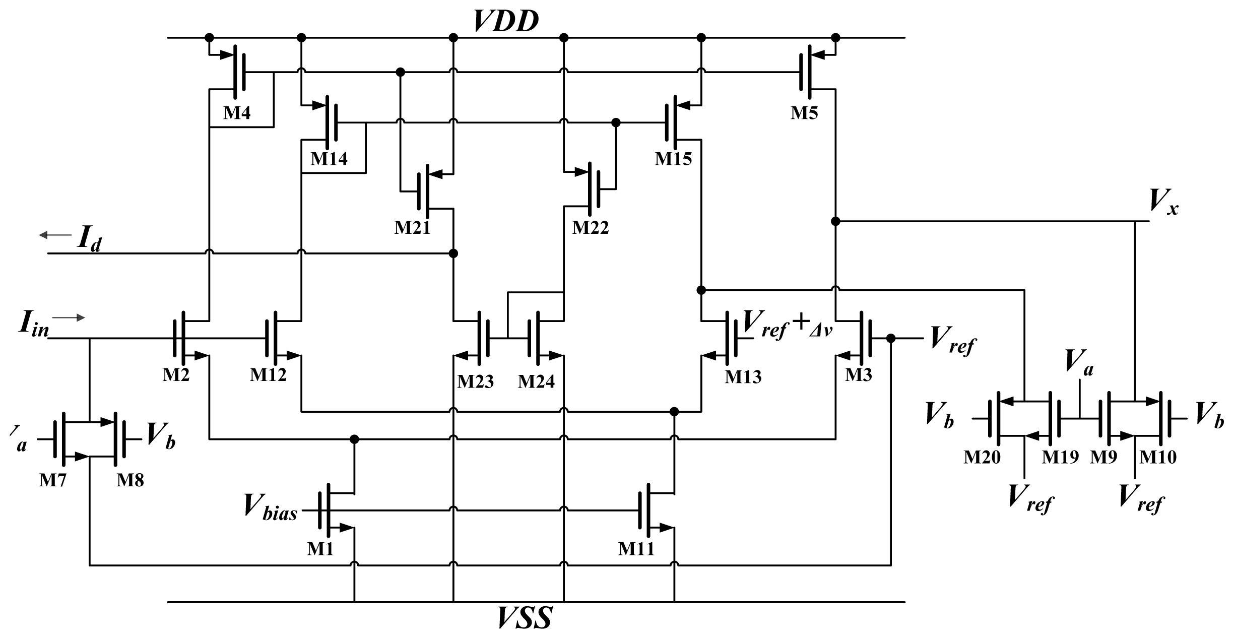
2.2. Neurons

A schematic diagram of the activation function circuit A and differential approximation circuit D are shown in Figure 6. The activation function was hyper tangent in this work. An analog circuit can easily implement the hyper tangent function using a differential pair [15]. As shown in Figure 6, the input current Iin is delivered through the synapse circuit and converted to voltage by M7 and M8. This voltage is compared with the reference voltage Vref, and an output current is produced. Because M2 and M3 operate in the subthreshold region, the output current is:
I x = I bias tan h ( κ ( V i n V ref ) 2 U T )
The output current Ix is then converted to voltage Vx by M9 and M10. This voltage Vx constitutes the output of the neuron.
According to the definition of differentiation:
f ( x ) = f ( x + Δ x ) f ( x ) Δ x f ( x + Δ x ) f ( x ) = f D ( x )
This study used the function fD(x) to approximate the actual differentiation f'(x) [12]. Consequently, this involved duplicating the activation function circuit (M12 and M13). The reference voltage for this replica differed from Vref by a small amount. The output current of this replica became:
I x _ r = I bias tan h ( κ ( V i n V ref + Δ V ) 2 U T )
The difference between Ix and Ix_r is the differential approximation of the activation function:
I d = I bias ( tan h ( κ ( V i n V ref ) 2 U T ) tan h ( κ ( V i n V ref + Δ V ) 2 U T ) )
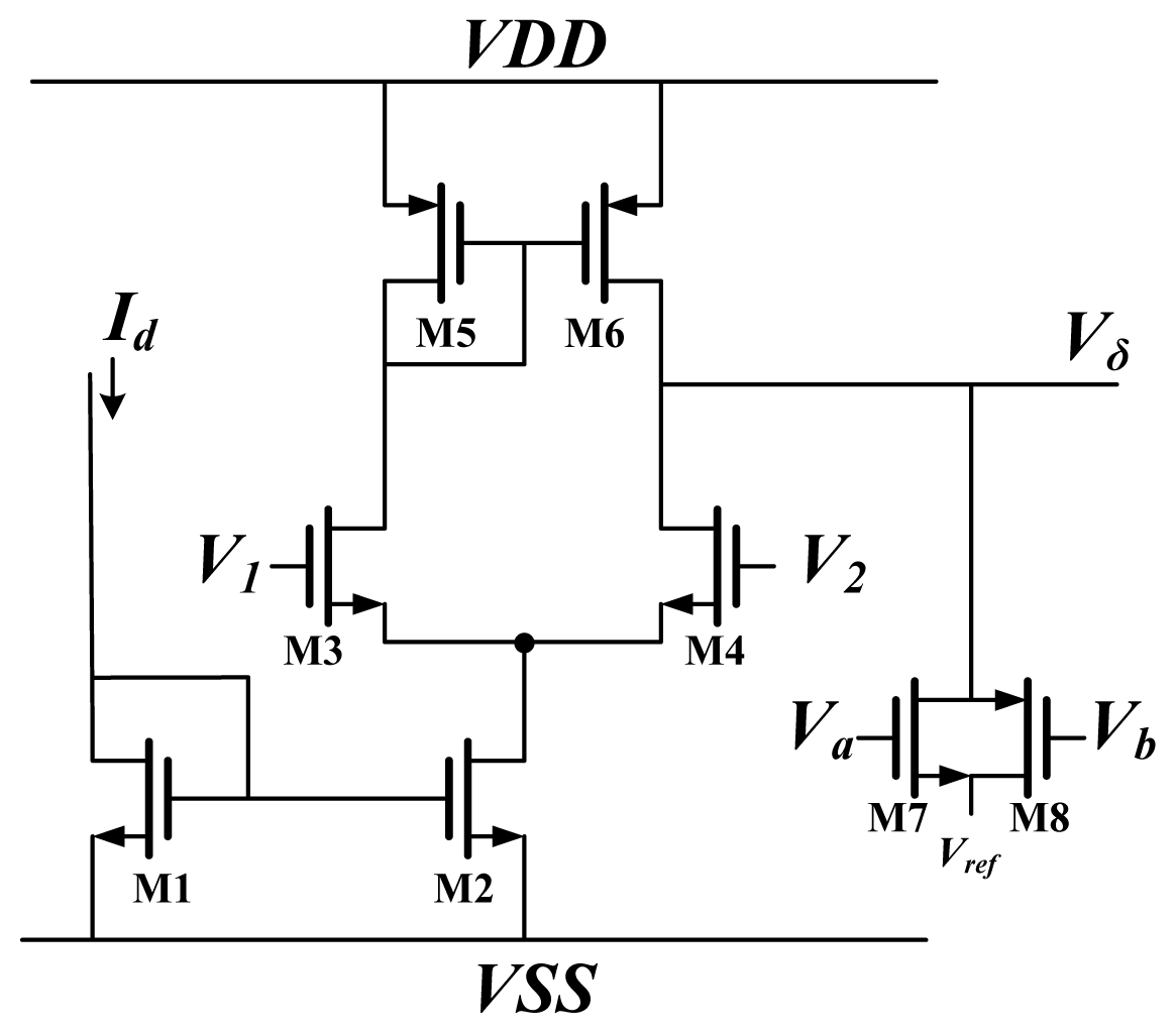
The schematic diagram of a Delta block is shown in Figure 7. It is used to times the back propagate error by the differentiation of activation function. The block is used to multiply the BP error by the differentiation of activation function. The differential approximation of the activation function is represented by current Id, and the BP error is represented by voltage. This circuit used differential pairs operated in the subthreshold region; thus, the circuit output was the same as Equation (5). For ON, V1 and V2 in Figure 7 are replaced by XO and Xt respectively. For HN, V1 and V2 were replaced by Vδ× W and Vref, respectively.

3. Results and Discussion

3.1. Experiment Setup

The entire system is shown in Figure 8. The system can be divided into three parts. The first part is the equipment for odor data collection. The data are collected and stored in a computer. The second part is the PCB for bias generation (PCB_bias). The third part is the designed chip.
An E-nose developed in a previous study [24] was used to assess fruit odor samples. Figure 9 shows the patterns of banana, lemon, and lychee odors, respectively. During the experiment, the temperature was between 24–28 °C and the humidity was 59%–78%.
We assessed 24 samples, and each sample was assessed individually. The E-nose had eight sensors [24], but the MLPNN chip had only four input channels; thus, four sensors were selected from the original eight. The data were normalized to a voltage between 0.85 and 0.95 V (to ensure the voltage range is sufficiently small for approximation in GM block to be valid) before being fed into the MLPNN chip. The E-nose in the previous study possesses metal-oxide sensors; consequently, the resistance of the sensor is reduced when odor molecules are combined with the sensor. The percentage of resistance change before and after the sensor responds to odor molecules is used to represent sensor activity. Consequently, the sensor response is initially an array with negative numbers. To perform normalization, first, the absolute value of the sensor response is noted. Second, each sample is divided by the maximum sensor response in the sample, and then is divided by 10; the sample becomes a vector with a maximum value of 0.1. Third, this vector is added by 0.85. Subsequently, every dimension in the input vector to the MLPNN chip is larger than 0.85 V but smaller than or equal to 0.95 V. The noise from the power supply is a critical issue for the analog circuit. Although certain research has reported that adding modest noise in synapse during training can improve the learning performance [25], the power supply noise must still be reduced because the power supply noise cannot be turned on during training and turned off during testing. Furthermore, the noise may be amplified by the circuit. With too much noise, the ANN may fail to converge [25]. Compared with a power supply instrument, a battery provides power with less noise. In this study, the chip was provided with power by a battery through a regulator. However, a battery provides a single voltage, whereas the chip requires multiple biases. To provide various biases of voltages from the same battery, this study designed a printed circuit board (PCB) to generate these biases. The circuits in this PCB contain regulators (Figure 10(a)) for generating power for the MLPNN chip and bias generators (Figure 10(b)) for generating bias voltage.
The MLPNN chip was fabricated using the TSMC 0.18 μm standard CMOS process with a 1.8 V supply voltage. The chip area was 1.36 × 1.36 mm2. The chip photograph is shown in Figure 11.

3.2. Odor Classification by MLPNN Chip

The learning ability of the MLPNN was tested through the following steps. First, the data were divided into two subsets, and one subset was used for training and the other for testing. Each subset contained 12 samples. Each sample was a voltage vector with five dimensions (fruit data and a teacher signal). These voltages were supplied by a data application device (NI PCI 6723). In the second step, the MLPNN was trained by these samples. A data acquisition device (NI USB 6229) sampled the weight values simultaneously and stored these data on a computer. The block diagram for training is shown in Figure 12(a). Although the training procedure includes a PC collecting neuron output and weight values, this is not chip-in-the-loop learning because the PC is not responsible for weight updating. The main goal of the PC is to provide long-term weight storage because the weight value in the storage capacitor in each synapse may decrease by the leakage current after a period of time. After training, a set of weight values was selected. During testing, the weights on the MLPNN were set to these values by the PCI 6723. The final step entailed applying the test data to the MLPNN, monitoring the neuron output, and verifying the results. The block diagram for testing is shown in Figure 12(b).

3.2.1. Training

During training, each sample sustained 40 ms; thus, this study sampled the weights and neuron output once every 40 ms. The charging and discharging period (learning rate) is set to 20 μs for each sample. To improve the learning performance of the system, each class was randomly applied. Because 12 samples are present, and each sample sustains 40 ms, the training epoch repeats every 480 ms. Figure 13 shows the neuron output during training. The red curve represents the teacher signal, and the blue curve shows the neuron output. The neuron output clearly differed from the teacher signal initially, but through training, the neuron output became increasingly similar to the teacher signal. By the end of training, the neuron output was almost the same as the teacher signal. Other than the neuron output, the learning result is also shown in the weight adaptation. Figure 14 shows the weight adaptation during training. The Hwij term represents the weight value of the synapse between the jth hidden neuron and the ith input neuron, and Ow1j refers to the weight value of the synapse between the output neuron and the jth hidden neuron.
The parameters in the circuit varied slightly because of the fabrication process; the majority of weight values converged, but a few did not. Thus, the final weights were not ideal values for testing. The class order during training was random. For example, the training order might be Ba-Ba-Le, while the order was Ba-Le-Ly (Ba means banana, Le means lemon, and Ly means lychee) on the other time. Our analysis showed that selecting the weight values after the sequence Ba-Le-Ly (or other combination of Ba, Le and Ly) could result in optimal classification. Thus, this study applied the weights obtained after Ba-Le-Ly to the MLPNN during testing.

3.2.2. Testing

The test results are shown in Figure 15. The class order during testing was Le-Ly-Ly-Ba-Ba-Le-Ly-Le-Le-Ba-Ly-Ba. The classification boundaries were set at 0.88 V and 0.92 V. When the output voltage was larger than 0.92 V, the input was classified to banana; under 0.88 V, the input was lychee; between 0.88 and 0.92 V, the input was lemon.
The Y-axis of Figure 15 is the output voltage of the output neuron. The X-axis shows different samples. For example, the first sample causes the network to produce an output voltage of approximately 0.9 V, between 0.88 and 0.92 V. Consequently, the first sample is classified to lemon by the network. Because the first odor data applied to the network is a lemon odor, the network correctly classified this sample. The results showed that only the third sample was misclassified, whereas the others were correctly classified. The testing accuracy was 91.7%. The power consumption was 0.553 mW.
The overall circuit specifications are listed in Table 1.

4. Conclusions

This study proposed an MLPNN chip using BP learning by the TSMC 0.18 μm standard COMS process. The use of an analog VLSI design with a simple structure meant that the proposed MLPNN had a relatively small size and low power requirements. The supply voltage to the chip was 1.8 V, and the power consumption was 0.553 mW. The measurement results showed that this design was capable of recognizing three fruit odors. Because of its small size, low power requirements, and accuracy in classification, the MLPNN chip can be integrated in a portable E-nose in the future. This would reduce the size and power requirements of the E-nose and would simultaneously increase the application field of the E-nose.

Acknowledgments

The authors would like to thank financial support of the National Science Council of Taiwan, under Contract NSC 101-2220-E-007-006. This work was also supported by the MediaTek Fellowship. The authors would like to acknowledge the support of National Chip Implementation Center (CIC), Taiwan for chip fabrication.

References

  1. Brezmes, J.; Fructuoso, M.L.L.; Llobet, E.; Vilanova, X.; Recasens, I.; Orts, J.; Saiz, G.; Correig, X. Evaluation of an electronic nose to assess fruit ripness. IEEE Sens. J. 2005, 5, 97–108. [Google Scholar]
  2. Blatt, R.; Bonarini, A.; Calabro, E.; Della Torre, M.; Matteucci, M.; Pastorino, U. Lung Cancer Identification by an Electronic based on an Array of MOS Sensors. Proceedings of the International Joint Conference on Neural Networks, Orlando, FL, USA, 12–17 August 2007; pp. 1423–1428.
  3. Lin, Y.J.; Guo, H.R.; Chang, Y.H.; Kao, M.T.; Wang, H.H.; Hong, R.I. Application of the electronic nose for uremia diagnosis. Sens. Actuators B Chem. 2001, 76, 177–180. [Google Scholar]
  4. Wang, L.C.; Tang, K.T.; Kuo, C.T.; Ho, C.L.; Lin, S.R.; Sung, Y.; Chang, C.P. Portable electronic nose system with chemiresistor sensors to detect and distinguish chemical warfare agents. J. Micro/Nanolith. MEMS MOEMS 2010. [Google Scholar] [CrossRef]
  5. Hong, H.K.; Kwon, C.H.; Kim, S.R.; Yun, D.H.; Lee, K.; Sung, Y.K. Portable electronic nose system with gas sensor array and artificial neural network. Sens. Actuators B Chem. 2000, 66, 49–52. [Google Scholar]
  6. Boilot, P.; Hines, E.L.; Gardner, J.W.; Pitt, R.; John, S.; Mitchell, J.; Morgan, D.W. Classification of bacateria responsible for ENT and eye infections using the Cyranose system. IEEE Sens. J. 2002, 2, 247–253. [Google Scholar]
  7. Koickal, T.J.; Hamilton, A.; Tan, S.L.; Covington, J.A.; Gardner, J.W.; Pearce, T.C. Analog VLSI circuit implementation of an adaptive neuromorphic olfaction chip. IEEE Trans. Circuit. Syst. I 2007, 54, 60–73. [Google Scholar]
  8. Ng, K.; Boussaid, F.; Bermak, A. A CMOS single-chip gas recognition circuit for metal oxide gas sensor arrays. IEEE Trans. Circuit. Syst. I 2011, 58, 1569–1580. [Google Scholar]
  9. Hsieh, H.Y.; Tang, K.T. VLSI implementation of a bio-inspired olfactory spiking neural network. IEEE Trans. Neural Netw. Learn. Syst. 2012, 23, 1065–1073. [Google Scholar]
  10. Hopfield, J.J.; Tank, D.W. Computing with neural circuits: A model. Science 1986, 233, 625–633. [Google Scholar]
  11. Morrie, T.; Amemiya, Y. An all-analog expandable neural network LSI with on-chip back propagation learning. IEEE J. Solid State Circuits 1994, 29, 1086–1093. [Google Scholar]
  12. Lu, C.; Shi, B. Circuit realization of a programmable neuron transfer function and its derivative. Proceedings of the IEEE -INNS-ENNS International Joint Conference on Neural Networks, Como, Italy, 24–27 July 2000; pp. 47–50.
  13. Gatet, L.; Tap, B.H.; Lescure, M. Analog neural network implementation for a real-time surface classification application. IEEE Sens. J. 2008, 8, 1413–1421. [Google Scholar]
  14. Lu, C.; Shi, B.; Chen, L. An on-chip BP learning Neural network with ideal neuron characteristics and learning rate adaption. Analog Integr. Circuit. Signal Process. 2002, 31, 55–62. [Google Scholar]
  15. Mead, C.A. Analog VlSI and Neural Systems; Addison-Wesley: Reading, MA, USA, 1989. [Google Scholar]
  16. Chible, H. Analog Circuit for Synapse Neural Networks VLSI Implementation, Electronics, Circuits and Systems. Proceedings of the 7th IEEE International Conference on Electronics, Circuits and Systems, Jounieh, Lebanon, 17–20 December 2000; pp. 1004–1007.
  17. Chiblé, H. OTANPS synapse linear relation multiplier circuit. Leb. Sci. J. 2008, 9, 91–103. [Google Scholar]
  18. Coue, D.; Wilson, G. A four quadrant subthreshold mode multiplier for analog neural-network applications. IEEE Trans. Neural Netw. 1996, 7, 1212–1219. [Google Scholar]
  19. Lont, J.B.; Guggenbuhl, W. Analog CMOS implementation of a multilayer perceptron with nonlinear synapses. IEEE Trans. Neural Netw. 1992, 3, 457–465. [Google Scholar]
  20. Milev, M.; Hrstov, M. Analog implementation of ANN with inherent quadratic nonlinearity of the synapses. IEEE Trans. Neural Netw. 2003, 14, 1187–1200. [Google Scholar]
  21. Rumelhart, D.; Hinton, G.; Williams, R. Learning representations by back-propagating errors. Nature 1986, 323, 533–536. [Google Scholar]
  22. Lu, C.; Shi, B.X.; Chen, L. An on-chip BP learning neural network with ideal neuron characteristics and learning rate adaption. Analog Integr. Circuit. Signal Process. 2002, 31, 55–62. [Google Scholar]
  23. Morie, T.; Amemiya, Y. An all-analog expandable neural network LSI with on-chip backpropagation learning. IEEE J. Solid-State Circuits 1994, 29, 1086–1093. [Google Scholar]
  24. Tang, K.T.; Chiu, S.W.; Pan, C.H.; Hsieh, H.Y.; Liang, Y.S.; Liu, S.C. Development of a portable electronic nose system for the detection and classification of fruity odors. Sensors 2010, 10, 9179–9193. [Google Scholar]
  25. Murray, A.; Edwards, P. Enhanced MLP performance and fault tolerance resulting from synaptic weight noise during training. IEEE Trans. Neural Netw. 1994, 5, 792–802. [Google Scholar]
Figure 1. Block diagram of the proposed 4-4-1 MLPNN.
Sensors 13 00193f1
Figure 2. Detailed block diagrams of HS, HN, OS, and ON.
Sensors 13 00193f2
Figure 3. Schematic of Chible's multiplier.
Sensors 13 00193f3
Figure 4. Schematic of Gilbert's multiplier.
Sensors 13 00193f4
Figure 5. The weight unit. (a) Training phase; (b) Classifying phase.
Sensors 13 00193f5
Figure 6. Activation function circuit and its differentiation.
Sensors 13 00193f6
Figure 7. Schematic of Delta block.
Sensors 13 00193f7
Figure 8. The photo of the components in the experiment. (a) Equipment for odor data collection; (b) PCB for bias generation; (c) socket and PCB with a designed chip inside.
Sensors 13 00193f8
Figure 9. Fruit pattern of (a) banana; (b) lemon; and (c) lychee odors.
Sensors 13 00193f9
Figure 10. The schematic diagram of the circuits in the PCB. (a) Regulator; (b) Bias generator.
Sensors 13 00193f10
Figure 11. MLPNN chip photograph.
Sensors 13 00193f11
Figure 12. The block diagram for training and testing: (a) training and (b) testing.
Sensors 13 00193f12
Figure 13. Neuron output during training.
Sensors 13 00193f13
Figure 14. Weight change during training.
Sensors 13 00193f14
Figure 15. Classification results.
Sensors 13 00193f15
Table 1. The circuit specification.
Spec.Value
Input Range (V)0.85–0.95
Output Range (V)0.82– 0.98
Power Consumption (mW)0.553
Chip Size (mm2)1.36 × 1.36
Accuracy (%)91.7

