Currents Induced by Injected Charge in Junction Detectors

Abstract
: The problem of drifting charge-induced currents is considered in order to predict the pulsed operational characteristics in photo- and particle-detectors with a junction controlled active area. The direct analysis of the field changes induced by drifting charge in the abrupt junction devices with a plane-parallel geometry of finite area electrodes is presented. The problem is solved using the one-dimensional approach. The models of the formation of the induced pulsed currents have been analyzed for the regimes of partial and full depletion. The obtained solutions for the current density contain expressions of a velocity field dependence on the applied voltage, location of the injected surface charge domain and carrier capture parameters. The drift component of this current coincides with Ramo's expression. It has been illustrated, that the synchronous action of carrier drift, trapping, generation and diffusion can lead to a vast variety of possible current pulse waveforms. Experimental illustrations of the current pulse variations determined by either the rather small or large carrier density within the photo-injected charge domain are presented, based on a study of Si detectors.1. Introduction
The drifting charge-induced current is often a prevailing component in detector signals. An analysis of this injected charge drift current is employed for the detection of photons or particles and for reconstruction of the electric field distribution over the charge drift area in detectors. However, the problem of the charge-induced currents remains a sophisticated issue in more complicated situations of photo- and particle-detectors when devices operate in partial or full depletion regimes with a complex field distribution in the presence of carrier capture-generation. Then, the induced current due to the charge trapping/de-trapping should be considered. The effects of the acting electric field screening or the gain caused by the interplay of the injected carrier charge and the bulk charge of ions in the depletion volume should also be involved. As usual, the principles of interpretation of the current transients in detectors under injected charge are based on the Shockley-Ramo theorem [1,2]. Ramo's theorem was derived based on consideration of Green's theorem and Gauss's law, thus, on the balance of electrostatic energy changes and on the analysis of bulk as well as of surface charge induced electrostatic fields. Ramo's current is derived at the assumption of the symmetry of an infinite electrode and of the spherical invariance of the potential surrounding an elementary charge. Therefore, the electrical capacitance of a real system of the finite surface area electrodes and its dependence on an applied voltage are out of consideration. Several attempts to generalize a simple Ramo's approach to multi-electrode and arbitrary space-charge field distribution systems had been made [3–6], although these solutions [3–13] are under debate, as referenced in [3–10]. As pointed out in [7], a simple Ramo's relation Equation (19) in [7] between the current within an external circuit and an introduced weighting field of geometrical sense is held only in the special case of moving charge in active area of a detector with a fixed external voltage applied. Therefore, a simple generalization or direct application of Ramo's theorem can be erroneous [7]. Most of the generalization approaches are again based on a consideration of electrostatic energy conservation [7–10]. For the space charge systems, like a pn junction and pin semiconductor devices, the simple Ramo's relations are not valid, and differential weighting potentials [8] are artificially introduced to restore the simple Ramo's type of expressions of the convection current. More systematic approaches are employed in [9,10], where space charge and different types of charges are included. However, the solutions obtained [9,10] for the estimation of the induced current on an arbitrary electrode provide no practical relevance of application with regard to semiconductor devices, as pointed out in [10], when the real velocity field of the charge domain is not known, and it should be evaluated by means of the complete analysis of field distribution. Thereby, an additional kinetic equation should be considered to determine the instantaneous velocity of the charge domain. However, applications of Ramo's theorem generally ignore this consideration, rendering the expressions obtained not practically applicable. The current pulse shape and duration are directly dependent on the temporal variation of the injected charge domain position within the inter-electrode space, where the instantaneous velocity and acceleration can be changeable. More complications appear within the consideration of a kinetic equation, when the injected charge amount can vary due to carrier traps inside the inter-electrode space.
In this work, the fixed area abrupt junctions with a plane-parallel geometry of electrodes are studied by considering the partial and over full-depletion regimes. The vectorial nature of the employed quantities of the surface charge domain, of the electric field and of the charge drift velocity is always kept in mind. The scalar relations are analyzed along the unite ortho-vector with proper signs ascribed to directions. To simplify the understanding of applied models, the single type of induced surface charge domain motion is initially considered. This simplification can be sufficient to model current transients due to highly absorbed photons or alpha-particles in Si detectors, while the generalization for a bipolar charge domain is also discussed. The specific features of the induced charge domain drift currents (ICDC) are revealed within analysis of the simulated ICDC transients and highlighted in illustrations of the experimental characteristics, measured on Si pin diodes.
2. Modelling of the Current Transients Induced by Injected Charge Drift
2.1. Geometry, Circuit and Electric Field Distribution for Different Regimes
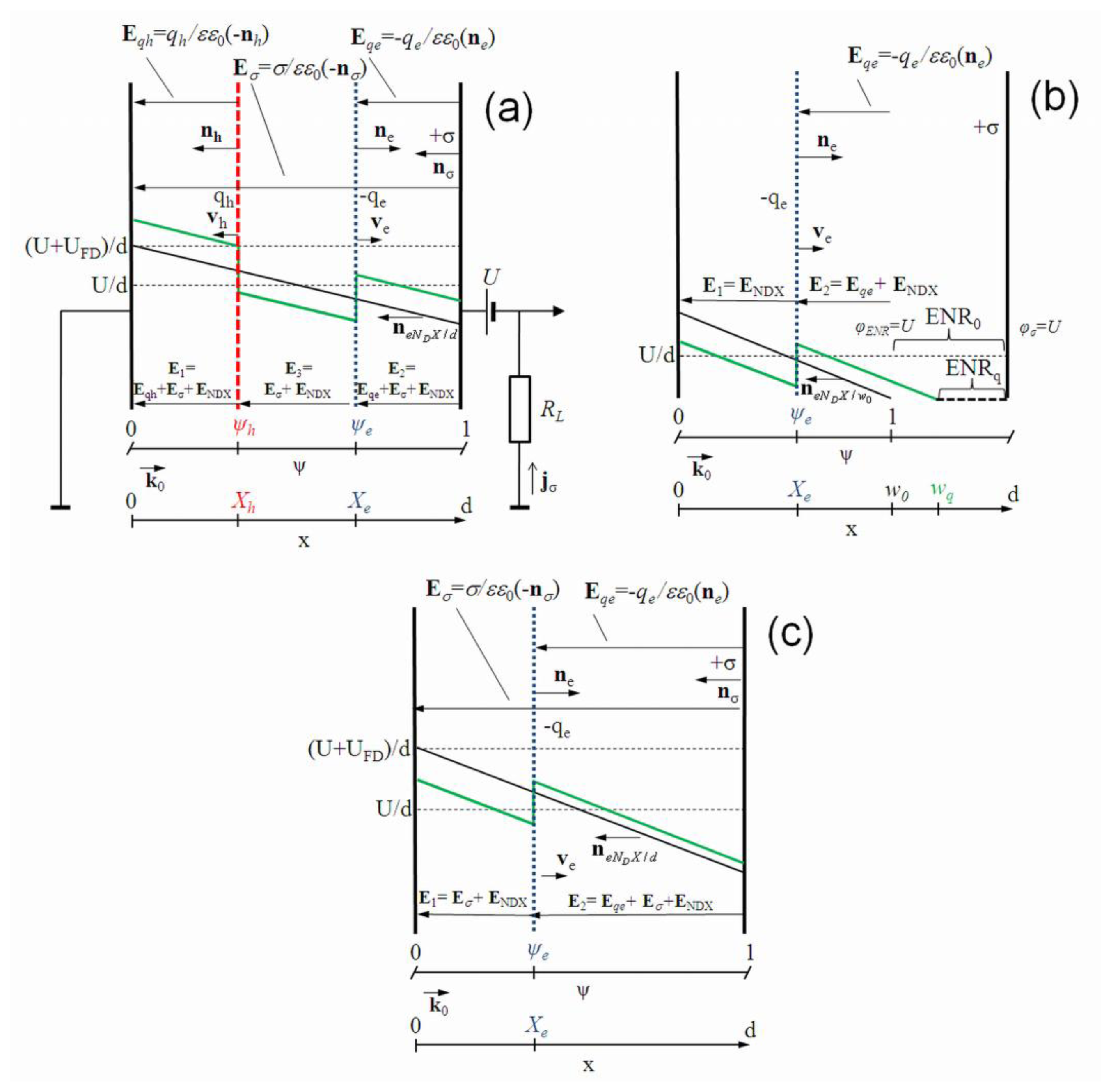
The same electrical circuit as in Ramo's theorem derivation, is considered: one electrode is grounded and the high potential is kept on the other one. These two electrodes are connected to the external voltage source in series with a load resistor to register a current transient within external circuit, as illustrated in Figure 1a. The circuit for detection of current transient i(t) routinely includes a load resistor and closed input of an oscilloscope type instrument. It is, as usual, assumed that the load resistor RL is properly chosen to get the recordable signal, and that a voltage drop on load resistor (iRL) for all the range of detected currents can be ignored, i.e., iRL ≪ U.
As usual, a quasi-neutral domain of excess carriers is initially generated in particle detectors. It is accepted the domains are flat surface vector quantities. These domains injected by light or ionizing radiation are characterized by the surface charge density and the direction (vector) of the surface normal. Thereby, these domains are directly represented by the electric field of the surface charge. The sign (polarity) of the injected charge and the direction of the drift velocity vector are also included. For the grounded circuit, the single-side surface charge (and field) is ascribed to the voltage source. The drifting domain is also considered as the one-side surface charge vector correlated with drift velocity vector direction. The surface charge electric field vectors are initially considered, like the first Poisson equation. Then, the scalar equations for an instantaneous field distribution are analyzed. By applying an external field source, the injected carriers (by light or ionizing radiation) can be separated into oppositely moving surface charge sub-domains qe and qh, which induce charges of opposite sign on electrodes. The positive charge on the grounded electrode induced by a drifting charge domain is moved by the external source (battery) to the electrode of the high potential and vice versa. The latter charge transfer current is actually measured within the external circuit as a signal of either the charge domain drift or the charge density change. A sketch of the instantaneous field components is presented in Figure 1.
External voltage source U produces a positive surface charge σ on the high potential electrode, which is positioned at the distance d from the grounded electrode. Specific for the junction type detectors, the mobile charges within an active volume of a device lead to varied depletion width w0 dependent on the applied (reverse Ur) voltage on electrode. The grounded electrode is assumed to be located at the beginning of the coordinate system (x = 0). The complete neutralization of the depletion charge (e.g., eND+) in the n-base active layer is obtained through respective depletion (wp+) of the other layer (eNA−) of a junction: eND+w0 − eNA-wp+ = 0. In the abrupt junction of a pin type diode, it is valid wp+ ≪ w0. Therefore, the assumption of the grounded electrode location at x = 0 is valid with precision of wp+/w0 ≪ 1. The injection of the electron domain, with surface charge density qe, into the active volume of a detector at the instantaneous position X0 causes a change of the charge on the high potential electrode, in the case of the over full-depletion regime.
For the partial depletion regime, this leads to changes of the depletion width wq, due to the mobile carriers in the electrically neutral region (ENR). As the electrodes are only connected to the external measurement circuit, the current induced by the moving charge –qe within the external circuit is determined by the surface charge dσ changes (being a full differential) in time: dσ/dt. To find these changes, the superposition of the induced fields should be considered.
The junction based detectors contain rather complicated field distribution, and, thereby, need specific analysis. The instantaneous field distribution in n-type conductivity region of the p+n abrupt junction structure during the monopolar drift of a negative charge in partially and over-depleted base region is sketched in Figures 1b, c, respectively.
2.2. Current Transient Induced by Charge Drift in Abrupt Junction
The analysis can be easily applied to the consideration of the barrier capacitance changes for unit area Cb = εε0/wq(t). The charge drift dependent depletion width wq(t) should then be introduced, due to the injected charge qe. The reverse biased steady-state depletion width w0 = [2εε0(U + Ubi)/eNDef] 1/2 serves as an equivalent of the inter-electrode spacing d. Here, Ubi denotes the built-in potential barrier, and Ndef is the effective dopant density. Variations of surface charge σ are equivalent to the changes of the surface charge at w0, induced by an additional depletion charge bar, as σ ∼ eNDef(wq(t) − w0). It can be proved that consideration of the time dependent changes of the system dynamic capacitance CSq (ascribed to a surface area unite) is equivalent to the analysis of the convection current. In semiconductor devices an important role is played by carrier capture and generation processes. Also, different regimes of the partial-depletion, of the full depletion and the over-depletion (depending on detector width and applied voltage) have their specific features. The mixed regimes of the electrode surface charge changes and of the depletion width variations are inherent for the applied voltage values close to the values UFD of the full depletion (FD). For clarity, these different regimes are separately analyzed below.
2.2.1. Current Transients of the Injected Charge Drift in Partially Depleted Detector
This regime is partially discussed in [14]. Let's consider a regime of the applied reverse voltages Ubi < U < UFD on the n-type conductivity layer at an assumption that the electron domain is injected nearby the metallurgic abrupt junction, and the strength of the electric field there is capable to separate the electron-hole pairs, with consequent extraction of holes into p+-type layer. This leads to a synchronous change of the depletion widths in the n- and p- type conductivity layers to keep the junction system electrically neutral behind the depletion w0,n and wp+ width boundaries. To simplify the analysis, an assumption of the asymmetric doping of n- and p-layers, i.e., the abrupt p-i-n junction is accepted, which enables ones to ignore a voltage drop on p+-layer. It is also assumed that the external metallic electrodes are in a rapid dynamic balance with neutral n- and p+- layer material. Thus, a rate of the processes within an n-layer region is the slowest one. The latter processes determine the current transient caused by a drift of the injected electron domain.
Using the methodology described in [14], an instantaneous field distribution is obtained by integrating the first Poisson equation and by assuming an infinitesimally thin drifting domain of surface charge of density qe, as:
Here, a vector of the electric field is directed towards the junction, while a surface charge domain of electrons can drift towards high potential electrode. To find a depletion width wq and, alternatively, E1(0), due to the injected charge qe domain and the external reverse bias voltage (Ur) source, the second Poisson integral should be taken, which leads to expressions:
Here, a common depletion boundary condition (E(wq) = 0) and a proper root of the quadratic equation are accepted; μ denotes the carrier mobility. For the reverse biased junction, it is assumed as usual [15] that U = Ur−Ubi. Within a coordinate system at rest, the characteristic time parameters τMq,w0 and τTOF,w0, are defined relative to a steady-state width w0, instead of d. Thereby, the characteristic time parameters τMq,w0 (time of the Maxwell relaxation of charge q, Mq) and τTOF,w0 (time of flight, TOF) are expressed as:
These characteristic times, namely, their equality (τMq,w0 = τTOF,w0), can be a measure for the validity of the electrostatic induction approach. These characteristic times implicate the response time of the extended (of distributed charge) electrode (τTOF,w0) and of a drifting domain (τMq,w0).
A steady-state depletion width w0 is expressed by a well-known formula derived within depletion approximation [15] as w0 = (2εε0U/eND)1/2. Consequently, a barrier capacitance is obtained as:
It can be inferred from Equations (1–6), that the regime of the surface charge domain drift within a partially depleted layer of a junction, can only be considered under a few restrictions on relations among values of the applied voltage, the doping and the injected charge density. A spatial range for wq variations is limited by a geometrical width d of a n-base layer (and consequently by the barrier capacitance decrease to its geometrical capacitance value), as:
For electrodes of surface unite area S = 1, this leads to the inequalities, written as:
Here, τM,Ndef = εε0/eμeNDef is the material dielectric relaxation time within a space charge region. Inequality Equation (8) leads to a limitation:
The rearranged (by these differentiation procedures) expression of a module of the current density of the injected charge domain (ICD) drift can be represented as follows:
The obtained scalar form of the current density within a coordinate system at rest (w0) is very similar to that of the Ramo's current expression. The main difference is an appearance of a coefficient Kτ, dependent on the dimensionless position Ψ* = Xe/w0 of a drifting surface charge domain within w0, and it is composed of the characteristic times as:
The appearance of the coefficient Kτ is a specific feature of the non-fixed position of the virtual electrode (wq), charge on which is varied by a changed depletion range of ions. Simultaneously, the possible drift length is also dependent on the rate of the formation of w0 and wq, i.e., on the characteristic time τM,Ndef = εε0/eμNDef = εε0/eμnENR of the stabilization of the transitional λ-thick layer (between the depletion and ENR layers) due to extraction of the mobile carriers nENR = NDef from ENR. This transitional λ layer is related to the Debye screening length [15].
The additional scalar equation (with properly accepted vector direction sign) for a velocity of the charge domain drift is now expressed as follows:
The rearranged equation into the dimensionless Ψ* = Xe/w0 form can be written as:
Extraction of the Ψ*(t) function, by integrating Equation (15), might be complicated [16], and it can commonly be found by a numerical solution. These solutions Ψ*(t) are only determined for an interval of the ζ values, evaluated by using condition [1 + ζ(τTOF,w0/τMq,w0)] 1/2 − ζ > 0. The same difficulty appears in evaluation of drift time tdr, implemented by inserting the second boundary condition Ψ* = 1:
Then, the obtained Ψ*(t) should be inserted into the right hand side of Equations (11) and (12). Actually, a direct numerical solution of Equation (14) might be preferable in order to simulate the current density transients. The initial component of a rise to the pulse vertex (jICD,F(t)) and the rearward relaxation component (jICD,R(t)) of a current pulse can also be modelled. Here, it is assumed for simplicity that the kinetic equation of motion Equation (14) is only slightly modified due to τMq,w0 during qe injection.
For Ne carriers located within a domain on its surface area Se, comprising a surface density qe = eNe/Se, the injected charge drift is assumed to be a uni-directional process. Therefore, to relate more adequately the characteristic times τTOF,w0 and τMq,w0, the inequality Equation (9) could be rearranged as:
Thus, for the partially depleted junction, both components d2/Se < 1 and (1−U/UFD) < 1 should be small, and these conditions ensure that τTOF,w0/τMq,w0 < 1. Actually, the correlated drift of the injected charge domain (as assumed for the Ramo's regime) can only be implemented at τTOF,w0/τMq,w0 ≈ 1. Thereby, the exact Ramo's regime is impossible for the partially depleted junction if Kτ ≠ 1.
Generally, variation of an initial component jICD,F(t) as a function of time t within the current pulse evolution is described for the time interval 0 ≤ t ≤ tdr as:
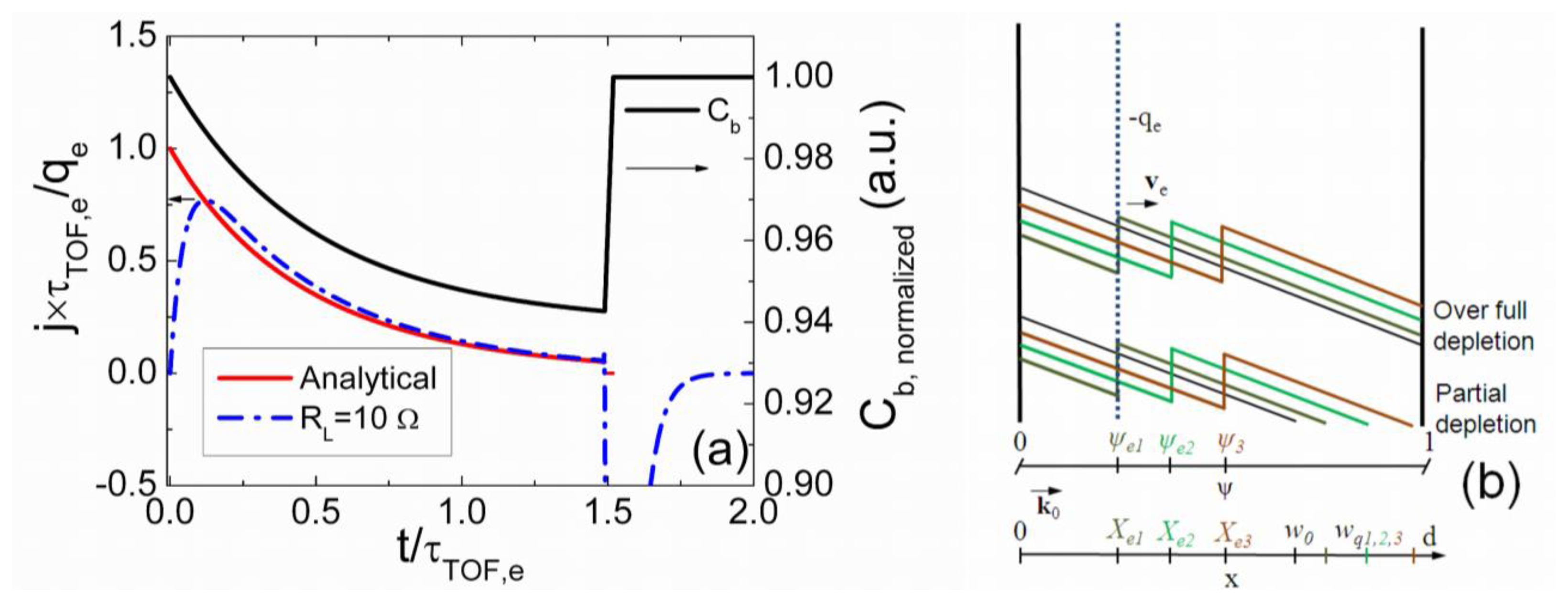
Equation (18) describes a component of the pulse with a decreasing current shape within the pulse vertex, Figure 2.
The rearward component (jICD,R(t)) (Figure 2) of the current pulse is determined by the processes of the system capacitance Cb,Sq restore to its steady-state value Cb,S0 = εε0/w0. At arrival of the drifting charge domain to the w0 location, the surface charge field qe/εε0 is equal to the electrostatic induction charge field determined by a depletion charge bar eND(wq−w0)/εε0. Therefore, the field qe/εε0 is completely screened being at w0, as the reverse voltage determined field of positively charged ions becomes zero at the point w0. Thus, from the time instant t = tdr, an interplay of carrier diffusion from electrically neutral region (ENR) and surface charge field qe/εε0 determines the reduction of the wq to the steady-state value w0. This process originates a current (relatively to a domain drift one) determined by narrowing of the depletion region, −carriers from the ENR drift into the opposite direction relative to the injected domain drift. This current represents the decreasing with time (t−tdr) component.
This current component may be responsible for the appearance of the offset within a current transient, inherent for the partially depleted detector. Duration of this process is determined by a dielectric relaxation time of the material, namely, τM,Ndef. This current flows until the instant tCw0 of the barrier capacitance restore to its stationary value εε0/w0. It is determined by the barrier capacitance charging current. Superposition of these currents leads to a current relaxation component expressed as:
As a result, the current density within a pulsed ICD transient is expressed as follows:
The offset current relaxation to zero is additionally governed by the parameters of the external circuit. The relaxation component of the current pulse is determined by the relaxation processes within an RC chain consisting of the system capacitance Cb,Sq and a load resistor RL. These elements together with the value of the applied external voltage determine the amplitude as well as the shape of the current pulse, and duration of the jICD,F and jICD,R components.
2.2.2. Current Transients in Fully Depleted Detector
The surface charge on a metallic (or heavily doped layer) electrode changes together with the space charge bar width due to a moving surface charge domain, when external voltage U is equal to or exceeds the full depletion (UFD) value, U ≥ UFD. This happens due to a lack of semiconductor material (supporting mobile carriers) width (relative to a partially depleted layer case) to withstand the action of the electric field due to the injected charge. The equilibrium carriers are extracted into the external electrode, if depletion covers completely the active layer width.
Again, using the methodology described above, a field distribution for the negative drifting charge is obtained by taking the first Poisson equation:
The solution for a scalar surface charge density on the high potential electrode is expressed as either:
The instantaneous field distribution can then be represented as follows:
It can be deduced from Equations (26 and 27) that similarly to the above considered structures, a capacitance of the system is decreased relative to its steady-state value, due to a drifting (Xe(t)) surface charge domain. It can be inferred a limitation for the charge density possible to move off:
This qe density also serves for evaluation of the relevant range of the positive capacitance CSNq values with qC = UCg = Uεε0/d.
A module of the current density, derived from Equations (26 and 27), in the case of the over full-depleted (OFD) junction, is again expressed as:
However, the considered situation for a fully-depleted junction is more complicated relative to those discussed above. The reason is a degenerated point wFD = d, Figure 2b. From one side, this is caused by the synchronous action of the capacitor-specific and the junction-inherent field distribution symmetries. As the junction determines a decreasing electric field shape, this field is exactly zero at the electrode (wFD ≡ d, the full-depletion condition) and σ does not change. Thus, any displacement current component for wFD = d, which is caused by the changes of an electric field behind the drifting domain, immediately becomes equal (transferred into) to a conductivity (convection) current, due to annihilation of the surface charge domain at Xe = d. But the symmetry of a capacitor-inherent field implies that the displacement and convection currents, flowing within a capacitor in opposite directions, exactly compensate each other to keep the external voltage invariable. The displacement current in the over-depleted junction is obtained as:
This jdispl (Equation (31)) component is different (through an additional eNDefdXe/dt type term) from that jOFD derived by consideration of the changes of a surface charge on the electrode of the capacitor. Actually, the current (displacement and drift) components measured within external circuit cannot be separated, while the complete current is determined by the changes of charge on the external electrode.
On the other hand, the displacement current (Equation (31)) eNDefdXe/dt and the conduction current en0dXe/dt components completely compensate each other: the displacement current is caused by a space charge bar eNDefΨed of ions, and the conduction current en0dXe/dt (Equation (31)) component, which appears due to a seeming extraction of equilibrium electrons n0 and by producing the surface charge en0d on electrode, contain the opposite signs in Equations (31). This peculiarity occurs, if the space charge bar (eNDefΨed) (either behind the injected surface charge domain (when Xe = 0) or in front of it (when Xe = d)) determines an appearance of the displacement current component to exactly compensate the conductivity current component en0d (to ensure invariance of external voltage U). Only for a singular set of boundary conditions U ≡ UFD and Xe = 0 as well as Xe = d, the displacement current εε0∂E/∂t is equal to ρE the material's conductivity current, i.e., εε0∂E/∂ t= ρE, where ρ represents a conductivity of semiconductor material.
Thus, the complete current within an external circuit is again determined by the displacement current due to the injected charge, as obtained in Equation (30). While the space charge bar induced displacement currents (within Equation (31)) are employed to exactly compensate the conductivity (convection) current component in a fully depleted junction layer. These peculiarities should be kept in mind when considering the field of velocities to express definitely the time dependent current changes within a current pulse.
A dimensionless velocity field can be considered by using the accelerating electric field component for a geometric width d of the inter-electrode spacing as:
The coefficients in Equation (32) can easily be rearranged by using the characteristic times:
These equations (Equations (36)) describe the changes of a dimensionless position 0 ≤ Ψ ≤ 1 with time in the interval of 0 ≤ t ≤ tdr for these three (A, B and C) regimes. The corresponding evaluations of a drift time tdr are obtained by using the relevant boundary condition (Ψ(tdr) = 1) for Equations (36). These evaluations of a drift time are expressed as follows:
These different regimes can be realized by varying the applied voltage U (through τTOF), the doping NDef (τM,Ndef) and the injected surface charge density qe (τMq). The first regime A (Equations (36 and 37)) is attributed to a small charge drift. Here, the time dependent variations of the dimensionless position Ψ(t) are similar to that of the partially depleted junction. These Ψ(t) contain a fast initial increase followed by a saturation character of the Ψ(t) changes when t approaches to tdr. The drift time is mainly determined by the injected charge dielectric relaxation time τMq, modified by a mismatch between τMq and τM,Ndef. The second regime B can be associated with a correlated drift of the surface charge domain, when Ψ(t) increases linearly with t, characterized by the invariable tdr, which is directly determined by τTOF. The third regime C is attributed to the large charge drift, when the injected charge is able to locally screen the depletion space charge of ions. Then, τTOF≅τMq < τM,Ndef, and the correlated (Ramo's type) drift of the injected rather large charge appears. The large injected charge determines the increasing drift velocity. Then, neither a drift velocity nor acceleration is constant. This leads to an exponentially rising (in time) current density during the charge domain drift time (0 ≤ t ≤ tdr). For this regime, the injected charge density is only limited by values qe < qC≅Cg(1 − UFD/U)U. The complete shielding of the external voltage created surface charge σ appears if qe > qC ≡ CgU. Only a diffusion of the injected carriers is then possible for qe > qC.
The current density ascribed to different regimes can be modelled by using the relevant expressions for Ψ(t), taken from Equations (32) and (36), in the drift velocity equation (Equation (32)). The current density is then expressed as:
The current density changes within a pulse vertex acquire a relaxation curve shape for the regime A, when screening of electrons (drifting charge domain) by ion charge within the depletion width prevails. For the correlated screening regime B, a square-wave shape current density pulse appears with a flat vertex. While for the correlated (Ramo's type) drift regime C (τTOF≅τMq), the transient with increasing in time current density is inherent.
The monopolar drift of holes can be expressed using methodology described above for the case of electrons drift. The positive charge qh drift is only possible towards the p+-layer. Then, the field for x < X0, which accelerates qh, is important for the consideration of the induction current. This yields:
The current density, for U = const, again acquires the Ramo's-type expression:
The drift velocity field is described by a differential equation:
Assuming the proper boundary conditions:
The monopolar drift time is then evaluated as:
The current density of the hole drift is expressed (by inserting Equations (41) and (46) into Equation (30) (modified for holes drift)) as:
In the case of the positive charge drift within n-base material, holes are always accelerated due to acting space charge field. The transient is then observed with the current density increasing with time.
2.2.3. Impact of Ion Space Charge in Fully Depleted Detector
The moving charge inside the over depleted space charge layer induces a displacement current component, which exactly compensates the conductivity current component, arisen due to a proximate contacting of the depleted layer with external electrode (outside layer). As can be inferred for the regime B (Equation (38)), characterized by the matched relaxation lifetimes τMq = τM,Ndef, the space charge eNDef over d accelerates a drift of the injected charge domain by the shortening of the drift time to the value tdr = τTOF/ [1 + (τTOF/2τM,Ndef)] < τTOF, for Ψ0 =0 (Equation (37)).
However, for the regime A of the non-correlated relaxation times of the space charge eNDef and of the drifting qe/d one, existence of the space charge eNDef leads to a reduction of the effective value of the drifting charge:
Then, a surface density of the drifting charge qe,ef is instantaneously and locally shielded by the space charge of ions, due to the rapid local reaction of the sufficiently large density charge of ions. Then, an increase ∼ exp[t/τMq] of the drift current density (Equation (38)) competes with a seeming reduction of the charge density qe ∼ exp[−t/τM, Ndef], caused by the ion space charge. The space charge of ions modifies the current density during qe drift by varying of length of the eNDefXe bar.
The large injected charge is able to locally screen the depletion space charge of ions, for the regime C. Then, a drift of the injected domain proceeds similarly to that in a capacitor-type device.
2.2.4. Bipolar Drift of Surface Charge in Junction Structure
As usual in detectors, a quasi-neutral domain of the excess carriers is initially generated. Then, owing to a steady-state applied field, these carriers can be separated into the oppositely moving surface charge sub-domains qe and qh. These drifting sub-domains induce charges on the electrodes and determine a field in between of them (qe and qh), to hold the initial quasi-neutrality. A sketch of the field components is presented in Figure 1a.
An instantaneous electric field distribution along the x axis (0 ≤ x ≤ d) for the bipolar drift can be represented as:
A field discontinuity at the instantaneous location of surface charge domains is expressed as:
Then, the relation between the surface charge +σ on high potential electrode and the external voltage U is obtained by taking the second Poisson integral. The solution for a scalar surface charge density σ can be written as:
It is worth to point out, that in the case of the bipolar drift, the charge σ on the high potential electrode becomes dependent on the instantaneous location of both electron and hole separated domains σ(Ψe, Ψh). This leads to the appearance of the fields acting on electrons (E2) and holes (E1). Theses fields also depend on the instantaneous location of the drift counter-partners as:
The induced charge current density, due to a bipolar drift, is expressed as follows:
It can be noticed that, owing to ve = −vh, the scalar current density can be represented by a sum of Ramo's-type components:
The bipolar drift velocities are correlated during the bipolar drift time τb (within time τb domain) as:
Here, the drift directions are included by accepting the relevant sign for the scalar velocity. There exist several situations of the pure bipolar and the mixed drift regimes. These regimes can be separated as:
The regime (Equation (57)) of the synchronous drift of both type carriers within the entire inter-electrode gap can only be realized for a single definite point of the charge domain injection Ψ0. While the mixed drift processes appear when the bipolar drift (within current pulse) changes to either the monopolar drift of the electron domain after holes reach a p+-layer or it becomes the monopolar drift of the hole domain after electrons reach the high potential electrode. These latter situations depend on the injection location Ψ0 = Ψ0h = Ψ0e within n-base region of the junction and on the mobility of carriers. In the general case of the junction structure, the drift process in both layers of the junction should be included. For instance, a drift of holes within n-base region should be extended into p+-layer of the abrupt junction to exactly account for the bipolar and monopolar regimes.
Pure Bipolar Drift
In the case of the pure bipolar drift regime (Equation (57)), a system of kinetic equations for the n-base region and their solutions are expressed as follows:
These solutions should satisfy the boundary conditions:
However, in the more precise approximation, the monopolar drift of holes within p+-region included by Ψ0 = Ψ0n + Ψ0p+, should be analyzed. Therefore, in rigorous consideration, the pure bipolar drift can be assumed as an idealization. Nevertheless, for the case of τtr,hp+ ≪ τtr,hn, the single layer approximation can be a relevant approach.
Then, the inherent time τb of the bipolar drift is obtained by integrating an expression for the drift velocity (using Equations (55, 57, 60 and 61)) as:
Inserting these solutions (Equations (60, 61 and 64)) into Equation (55), the current density (in the case of the pure bipolar drift) is expressed as:
Thus, the pure bipolar drift leads to an invariable current density with pulse duration of tP≅Ψ0τTOF,h, Equation (65), provided that carrier capture can be ignored. The dimensionless position of the charge injection always is Ψ0 ≤ 1. Therefore, the injected charge drift current pulse is even shorter than a time of flight of the counter-partners in bipolar drift, i.e., either tP < τTOF,h or τTOF,e(1−Ψ0).
Bipolar Drift During Hole Drift Time
In the case of the hole drift time τtr,h is the shortest one among the characteristic times, a bipolar (τbB =τtr,h) drift (Equation (58)) is described by a system of the kinetic equations and their solutions, which can be presented as follows:
These solutions should satisfy the boundary conditions:
Here, Ψe*0 serves as the start position for a drift of the electron domain, just during an instant of disappearing of the domain of holes at the grounded electrode. The time τbB of the initial bipolar drift is obtained by integrating the expression for the drift velocity (using Equations (66–69 and 55)), as:
Here, the step-like change of field and current density would have obtained for an instant of hole arrival to the grounded electrode. To validate the charge, charge momentum, and energy conservation, the coordinate transform should be performed, to stitch the solutions obtained in the moving (τbB time domain) coordinate system to that obtained (Equation (30)) for the system of coordinates at rest. This transform should include the charge induction on the electrodes, the drift velocity conservation and the coordinate relations, which can be represented as:
These transforms relate the “new” Ψ+ coordinate in the system at rest with that Ψ (within bipolar drift time domain) moving one for the proceeded monopolar drift analysis, after the charge induction procedure is accounted for, and velocities are matched. Then the prolonged monopolar drift velocity of electrons (for the case when τMq,e < τM,Ndef) is expressed as:
Here, Re1 and Re2 are the lifetime ratios, which can be dependent on the voltage drop sharing; v0,e,mon is the initial velocity of the monopolar electron drift, which is obtained using relations of velocity vectors and their directions for bipolar drift and for the re-calibrated monopolar drift as:
This gives a coincidence of v0,e,mon and vΣbip|Ψe*0 values at the position Ψe*0 of an electron domain. Expressions for the function ψ(t) and monopolar drift time are obtained by integrating (Equation (75)) expression with the initial and boundary conditions:
These solutions are given as:
The entire duration tP of the current pulse contains the both phases:
The current transient (for the analyzed case of τMq,e < τM,Ndef) has a decreasing current component within the initial phase (during a bipolar drift) and an increasing one within the rearward component of the transient due to a drift of the electron domain which screens the space charge. For the case when τMq,e = τM,Ndef, the electrons drift with the constant initial velocity v0,e,mon due to a compensation of the drifting charge and the space charge fields. For the case of τMq,e > τM,Ndef, the electrons drift with a decreasing velocity, as the large space charge of ions (relative to a drifting charge) screens the drifting charge.
Bipolar Drift During Drift Time of Electrons
In the case the electron drift time τtr,e is the shortest one among the characteristic times, a bipolar (τbC = τtr,e) drift is followed by a monopolar drift of holes towards p+ layer of the junction. After performing analogous (as described in previous section) coordinate transformations and solving drift velocity equations for the bipolar (during drift time of electrons (Equation 59)) and prolonged monopolar drift of holes, the current density is expressed as:
Here, Ψh*0 denotes the initial domain position within the monopolar drift of holes; v0,h,mon is the initial velocity of the monopolar hole drift which is obtained using the relations of velocity vectors and their directions for the bipolar drift and for the re-calibrated monopolar drift as:
In the case of the proceeded hole monopolar drift within n-base material (after the phase of the bipolar drift is finished), holes are always accelerated due to the acting space charge field. The hole drift with an increasing velocity determines an inherent shape of the increasing current density within a transient, during the monopolar drift phase.
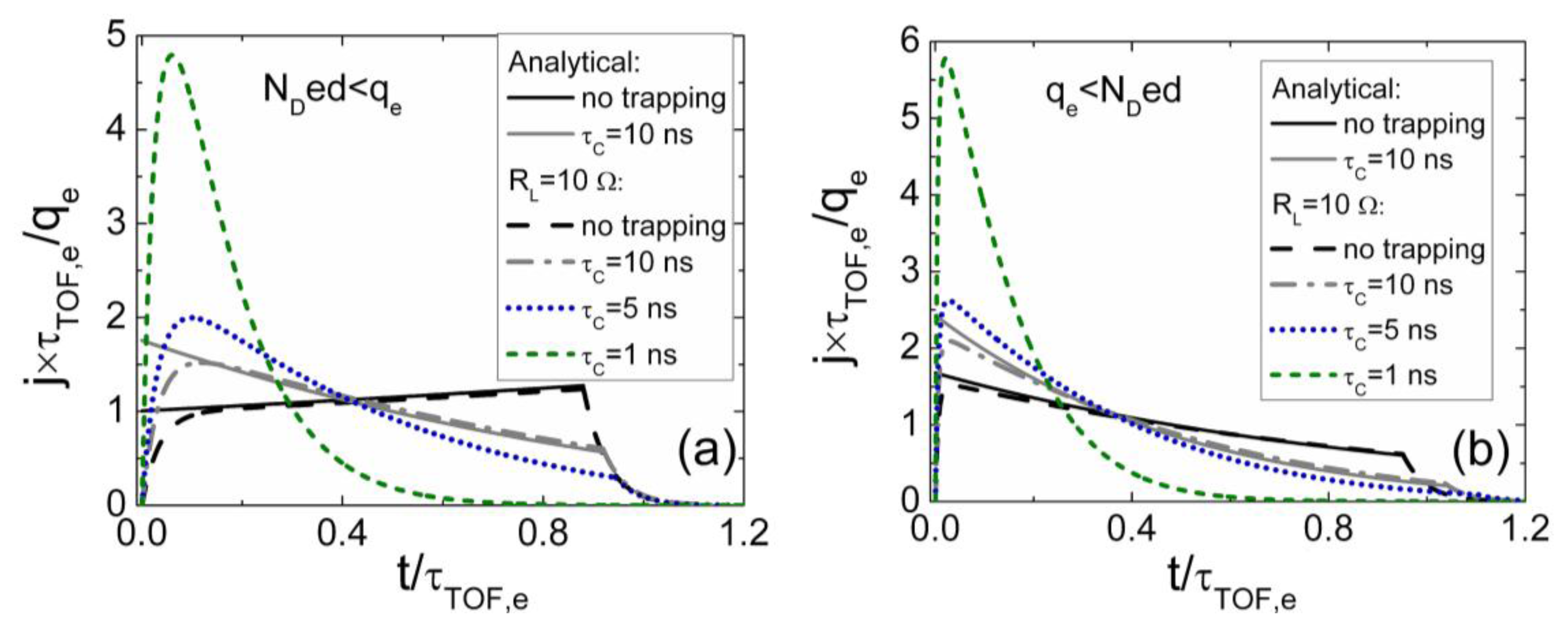
3. The Impact of Carrier Trapping and Generation
3.1. The Impact of Carrier Trapping
The injected charge current can also be changed by carrier trapping and generation. The surface charge density dependence on time for the simple traps can be expressed as:
Introducing a trapping dependent dielectric relaxation time as:
Here, the time dependent quantities of NDef(t) and qe(t) should be employed. Capture of the injected excess carriers, as usual, leads to a synchronous filling of empty donor and acceptor type traps those determine the overall charge neutrality and effective doping NDef. Then, the current density within a pulse, at assumption that NDef(t)= NDef0exp(−t/τC), is expressed as:
This equation should be properly matched with the drift kinetic equation:
The latter equation can only be solved numerically, although the general solution [17] can be expressed through complicated integrals [16].
A few aspects of the impact of carrier trapping on the injected charge transients for a partially depleted junction layer have been mentioned in [14,18]. Evaluation of other parameters (e.g., tdr) of the transients determined by the injected charge drift and trapping becomes even more complicated, and it can be implemented only by the numerical methods. For prevailing of trapping processes, no articulated features of the detector response ascribed to the injected domain drift can be separated, and only the relaxation-type shape followed the charge domain injection peak can be observable within a current transient.
No drift exists (∂Ψ/∂t ≅ 0) and, consequently, Ramo's current component disappears, if a trapping lifetime of the induced charge qe0 domain is the shortest one within a set of characteristic relaxation parameters. Then, equation (Equation (91)) for current density can be simplified as:
3.2. Generation Current Component
Carrier trapping, associated with a drifting surface charge domain, may determine the immediate (during time significantly shorter than other characteristic time parameters) and local changes of the effective charge. A decrease of NDef due to a filling of the charged donor-type traps is equivalent to a local charge generation. Thus a simplified approach for evaluation of the generation current can be considered. Then, carrier trapping and generation can be analyzed synchronously by rearranging Equation (88) as:
Here, m0 denotes the initial carrier density on filled traps or the density of the neutralized donor-type traps, e is the elementary charge, and τg,ef is an effective generation lifetime. At these simplified assumptions, Equation (94) can further be rearranged as:
This simplified approach enables one to include into consideration the local charge generation. Unfortunately, the solutions can be obtained only by numerical analysis.
The discussed above simplified analysis of the components of carrier drift, trapping and thermal release enables one to make the rough estimations of the impact of different components. However, the rigorous consideration of processes should be based on the causality principle. The current changes can only appear during or after injection of qe. Therefore all the relations for the electric fields and charges caused by qe, obtained within the electrostatic approach, and containing the time dependent qe(t) components should appear as the convolution integrals, for instance, as:
This specification leads to the integral-differential equations. These equations can only be analyzed numerically. Then, the above presented simplified models can be employed for the initial and qualitative prediction of the numerical solutions.
4. The Role of Carrier Diffusion
The drift velocity is varied through the electrostatic interaction of injected charge qe and surface charge σ on electrode, due to external voltage source. The initial zero drift velocity actually appears when the detector signals are caused by the secondary electron-hole pairs generated by the energetic elementary particles (high energy photons, hadrons, etc.). Then, a neutral domain with an equal density of electrons and holes in pairs is locally generated. The external field is able to separate and move these counter-partners towards opposite directions if the density of these carriers is less than qC, i.e., for qe < qC = CgU.
In the partially depleted junction layer, for U ≤ UFD, the current (ascribed to the injected charge drift) varies due to the temporal changes in wq(t), and it really contains a pair separation Xe-h(t) = Xe−Xh length. The charge separation process induces the change of the depletion width wq (an increase, relatively to its steady-state value w0,n&p+) in both layers of the junction, i.e., wq,n and wq,p+. The extracted excess holes are located at p+-side producing the same value of the surface field. Thus, the overall charge balance wp + N-A,p+ = wnN+D,n together with qh,p + X0,p+ = qe,nX0,n is maintained in a diode for the moderate density of the injected charge domain. In the heavily doped layer, the characteristic times, e.g., dielectric relaxation times, are significantly shorter than those in the resistive layer. Therefore, current transient pulse duration is mainly determined by the longer processes within more resistive layer. This motivates an approach of a separate consideration of electron drift within a base region of the reverse biased diode detector, where a charge separation process is assumed to be sufficiently short, and a drift starts after extraction of counter-partners (separation of pairs) process is finished.
In the general case of the local injection of excess carrier pairs, separation of counter-partners depends on their densities. The external source induced charge σ on electrode can be completely shielded by the large injected charge qe within a Debye screening length during the dielectric relaxation on metallic electrode, which is extremely short. The space charge of ions is also screened during τMq, which is then the shortest one among the characteristic times, in the case of qe ≫ eNDefd and (qe/ε0ε)d > U. The external source is able to react by changing σ, till the system capacitance is CSq > 0. However, the large injected charge qe nearby the grounded electrode (X0 ≅ 0) is able to create an internal field and a voltage drop (qe/ε0ε)d, which reduces the dynamic capacitance of the system to CSq = 0. Then, the external voltage source is completely blocked in supporting of σ. As a result, no separation of the electron-hole cloud (into domains of electrons and holes) appears. Thereby, relaxation of the injected quasi-neutral domain happens completely by carrier diffusion process.
The reason is the excess carrier diffusion and appearance of the diffusion induced inner field [19] as:
This field is proportional to the excess carrier density gradients. For the locally generated domain of the nearly infinitesimal width (for instance in tracking of hadron path) within significantly wider inter-electrode gap of detector, diffusion due to a sharp gradient (which is also proportional to the carrier density) induces an inner electric field which balances a further widening of the domain. Strength of this field can be sufficient to compensate partially or fully the applied external field (surface charge σ) in the case of low applied voltage and the rather high densities of the injected carriers. Then, carrier diffusion and drift leads to the outspread of the domain. Such a process is characterized by the ambipolar diffusion coefficient Da. In thin detectors with small applied dc voltage, a width of the outspread domain can approach the geometrical dimensions of the inter-electrode layer, even when it is formed by the strongly absorbed radiation. The same situation can be realized by the photo-injection of excess carrier into a rather thick detector using the homogenously absorbed light. Then, the injected domain sweeps the inter-electrode spacing. The external electric field acts as the accelerating factor for the surface recombination sd/D (of velocity s, related to sd/D = d/LD by Debye screening length LD). This problem is very similar to the excess carrier ambipolar diffusion moderated carrier recombination on surfaces. Then, action of the external field and carrier drift can be included into the properly modified surface recombination velocity s. Solution of this problem is well-known [20–23], and it leads to a transient of conductivity current due to the carriers arrived to the electrode and extracted to its surface. Time variations of the excess carrier density in this domain (averaged over the geometrical thickness d of inter-electrode space) is expressed through a sum of the space mode ηm components as:
The space frequencies (η) of these decay modes are described by the solution of the transcendental equations of type:
Here, s1 = LD,h/τTOF,LD,h and s2 = LD,e/τTOF,LD,e denote the surface recombination velocities ascribed to the electric field caused extraction of carriers towards the front and rear (surfaces) electrodes (with relevant Debye lengths LD,h, LD,e), respectively. These (Equation (102)) solutions with roots found from Equation (103) predict a two-componential, the relaxation type current transient. Such a transient contains the initial non-exponential relaxation component. The asymptotic decay component is characterized by the time parameter τD = 1/η12D of the main decay mode, representing the effective time of the domain dissipation,— due to diffusion over the entire inter-electrode spacing.
5. Current Transient Changes Determined by a Signal Recording Circuit
A signal registration circuit (namely, load resistor) inevitably transforms the current transient shape. This appears due to the voltage sharing and the consequent change of a voltage drop on detector depending on current value within the circuit. In more general case, the transients are described by the solutions of the differential equation with variable coefficients, derived as:
This leads to a differential equation:
The changes of a system dynamic capacitance determine the initial delay and the final stage (relaxation) components within the simulated transient. These components are inevitable within the charge drift current transients, recorded in experiments. Also, these components should be included into the evaluation of the charge collection efficiency. Depending on the geometrical capacitance (Cg) and load resistance (RL) values, the current pulses are significantly modified.
6. Discussion
The simplified models [23,24], based on Ramo's expression for the drift current, are attractive as they provide a simple analytical description of the detector signals. However, the analytical expressions can only be obtained for the simplest approximations. The analytical form of the correlated drift (Ramo's-type) current for the junction type detectors is only applicable for a primary estimation of a transient shape. Different regimes in the formation of the pulsed response of detectors can appear in a real measurement. The time-dependent variations of the current transients may be determined by the injected charge dissipation through the domain drift, dielectric relaxation (due to media polarization effects), through carrier capture and thermal release processes in the traps containing material, via ambipolar diffusion processes. Several specific aspects of these phenomena have been discussed above.
6.1. Limitations of Models
Adaptability of the simplified models presented above is additionally limited by several factors. A principal limitation leads to the threshold values of the acquired drift velocity that should be significantly less than those of the electric field (light) propagation velocity in the material under consideration, to ensure the validity of the electrostatic approach. This condition excludes the possibility to detect the primary charged particles (moving with relativistic velocities) within the inter-electrode spacing. Thus, the secondary particle (the electron-hole pairs with a zero initial drift velocity at the injection point) induced currents should be calibrated to the primary particle impact. The specific feature of the prevailing drift current caused by the monopolar charge domain is the increase of the drift current with time within the vertex of a current pulse. To separate the neutral domain (locally generated) into the drifting charge sub-domains, the sensitivity threshold for the applied voltage appears. This limitation leads to a condition of the elevated values of bias voltage, at least U > Ubi for the partially depleted semiconductor detectors. An enhancement of the external voltage may lead to the carrier velocity saturation, which complicates the analysis of the drift velocity field: vdr(Xe). Values of the highest external voltages are also restricted by the necessity to exclude repeated and non-linear drift processes, —such as the photo-electric gain moderated by carrier trapping and the avalanche processes of the impact ionization or Pool-Frenkel effect.
6.2. Limitations in the Evaluation Precision of the Depletion Layer Boundary
In the analysis of the junction type detectors, the parabolic approach has been employed, which relates the applied voltage and the width of the depleted region, and it is routinely exploited in device physics [15,25]. This approach enables one to simplify the expressions for the electric field description, as discussed in [15]. But this approach limits the precision in evaluation of the characteristic widths of w0, wq and wFD. In the steady-state case, the Debye screening length LD can be a measure for the evaluation of the precision in the estimation of w0. Thus, the transition layer [15] width, expressed as:
The transitional layers are actually inherent to the boundaries between the metallic electrodes and dielectric or external heavy doped layers of junctions. Owing to a short dielectric relaxation in the heavy doped layers, the semiconductor junction is preferential relative to a dielectric in between of electrodes.
6.3. The Impact of the Injected Charge Density
In the Ramo's derivation of the charge drift current, it was clearly proved the reciprocity principle: the reversibility and equality of the mutual action and reaction of the charged electrode and drifting charge. This is based on the conservation of the charge (σ induced electro-statically on the electrode plane by a drifting injected charge q = δσ), charge momentum qdΨ/dt (qvdr) and the electrostatic energy (qΦ = σ U). Here, Φ is the surface equi-potential surrounding the drifting charge. The main equation for the current density (for instance, considering the motion of the electron domain) can be directly obtained by using the electrostatic energy balance δqΦ = −δ(σU). Here, δ means a change in the electrostatic energy due to a variation of the surface charge (δσ) on the electrode, which should be balanced by a change in the energy of the moving charge qe. In the latter balance, qe is assumed to be invariable, and these energy changes are ascribed to the changes of the potential δΦ(Xe), —during charge drift. The temporal changes of the surface charge on the electrode gives current density variations dependent on time (for a fixed external voltage), and this current density is generally expressed as j(t) = dσ/dt = −(qe/U)(dΦ/dXe)(dXe/dt). Accepting the general electrostatic relation E= –gradΦ = neqe/εε0 = Eq and assuming that instantaneous Eq(Ψe) = qeΨe/εε0, for its scalar representation, the expression for the current density is rearranged as j(t) = dσ/dt = qe(d2/U)(qe/dεε0)[d(Xe/d)/dt] = qe(τTOF,e/τM,q)[d(Xe/d)/dt]. Thereby, the just derived current density (on the basis of electrostatic energy conservation in the case of our consideration) is consistent with Ramo's derivation (also made on the basis of energy conservation) if τTOF,e/τM,q = 1. On the other hand, the equality of τTOF,e and τM,q is consistent with electrostatic induction approach. Using the scalar values of the field within the inter-electrode space as Eσ = U/d and divEq ≡ ▽·Eq(Ψq) = qe/εε0d, for the injected charge field Eq (over a geometrical width d), and a balance of electric fields and Eσ = U/d = divEq ≡ ▽·Eq(Ψq) = qe/εε0d, one gets a weighting field WE = divEq/Eσ = d−1. This result validates the equal action and re-action of the surface (σ and q) charges and leads to the equality of the response times τMq,e = τTOF,e. Actually, the equality of the response times τMq,e= τTOF,e is ensured due to correlated changes of the acting voltage which is varied with Ψ(t). To find the drift velocity field vdr(Xe) = dXe/dt, the problem should be solved by consideration of the fields and charges in details.
As it has been demonstrated above, the drift velocity vdr is a function of the instantaneous charge domain position and the characteristic times: τTOF,e, τM,q and τM,Ndef. It can be proved that the current density j(t) = 9εε0μU2/8d3 obeys Mott-Gurney's law [26,27], for vdr(Xe = d/2) = μ [(U/d) + (qe/2εε0)]. Therefore, all the applied voltage U drops within the gap between the high potential electrode and the qe domain, during the initial phase of a drift process. The drifting domain additionally acts as a voltage sharing element (divider) with the parabolic-like characteristic of U2 = (1−Ψ2)U. As a consequence, the drifting charge coordinate Ψ(t) ∼ exp(t/τMq) increases exponentially with the drift time t, leading to a variable drift velocity vdr ∼ dΨ(t)/dt) ∼ (d/τMq)exp(t/τMq) and the acceleration a(t) ∼ (d/τMq2)exp(t/τMq), to hold the processes (of drift, voltage sharing, and the induced amount of charge) correlated in time. In the case of the pure bipolar domain, the correlated drift of qe and qh sub-domains is equivalent to a widening of the quasi-neutral e-h domain.
In real detectors, the prevailing regime is the detection and collection of a small drifting charge, where τMq,e/τTOF,e ≫ 1. Unfortunately, this regime can only be approximately considered within the one-dimensional approach. The reason is a slow dielectric relaxation (τMq,e/τTOF,e > 1) of a small drifting charge qe. Due to the small qe, the charge domain surface becomes corrugated under the action of the electrode charge (at boundaries of the detector electrode of finite surface area S) and the charge density gradients within the surface plane of a drifting domain. To stabilize the gradients (or the oblique action of σ surface segments), the drifting charge should vary its position in all three spatial dimensions. Thus, the lateral fields should be taken into account, —the charge of dangling bonds on perpendicular boundaries acting as the surface recombination sinks can be a reason for such fields. On the basis of the Lagrange variational principle, it can be understood that charge movements within both the electrode and the domain planes should be correlated, to react most rapidly on each others changes. Then, energy conservation can only be considered by an analysis of the three dimensional charge drift and diffusion problem. This leads to the appearance of charges and their neutralization currents on the perpendicular (to an inter-electrode drift direction) boundary planes of the base region of the junction type detector. The small drifting charge qe is able to terminate the electric field of the electrode's equal to its amount. Therefore, a small drifting charge acts as a linear voltage divider within the inter-electrode gap, and, consequently, the I-V characteristic obeys Ohm's law. Then, due to the charge drift, the acting voltage is different from that applied on electrode U, and it changes under the variation of the charge position. The small charge drift current density is less (in comparison with the regime of the large charge drift) due to the less effective voltage Uef, acting on the injected charge, qe. This leads to the increased τTOF,e(t). The approximation models for Uef should be applied to cover the entire range of the injected charge values. Namely, for an electron domain the ratio Re1 = τMq,e/τTOF,e and Re2 =τMq,e/τM,Ndef should be replaced by Ref,e1 = (τMq,e/τTOF,e)(Uef,e/(U + UFD)) and Ref,e2 = (τMq,e/τM,Ndef)(Uef,e/(U + UFD)) (which modifies the voltage) using the approximation Uef,e = 1.225qed(Ψe*0)1/2/εε0. Here, Ψe*0 is the dimensionless location of a drifting domain at the end of a bipolar drift. While, for a hole domain drift, these are Ref,h1 = (τMq,h/τTOF,h)(Uef,h/(U − UFD)) and Ref,h2 = (τMq,h/τM,Ndef)(Uef,h/(U − UFD)) (which modifies the voltage) using the approximation UC,ef,h = 1.995qhd(Ψh*0)1/3/εε0. These approximations can be understood by an equal redistribution between degrees of freedom for the three-dimensional motion, if Re,h ≠ 1. The applicability of the Uef approximation models has been verified by their relevance to stitch together the one-dimensional solutions of the bipolar and the monopolar drift, thereby matching the synchronous conservation of the charge, charge momentum and current density continuity. This enables one to get continuous current density variations within the simulated vertex of the charge drift current pulse.
6.4. Correlation with Experimental Results
As mentioned above, a vast variety of possible pulsed current transients, composed of drift, diffusion and displacement current components exists depending on the detector design and different external factors, such as the injected charge quantity, applied voltages, presence of traps, etc.
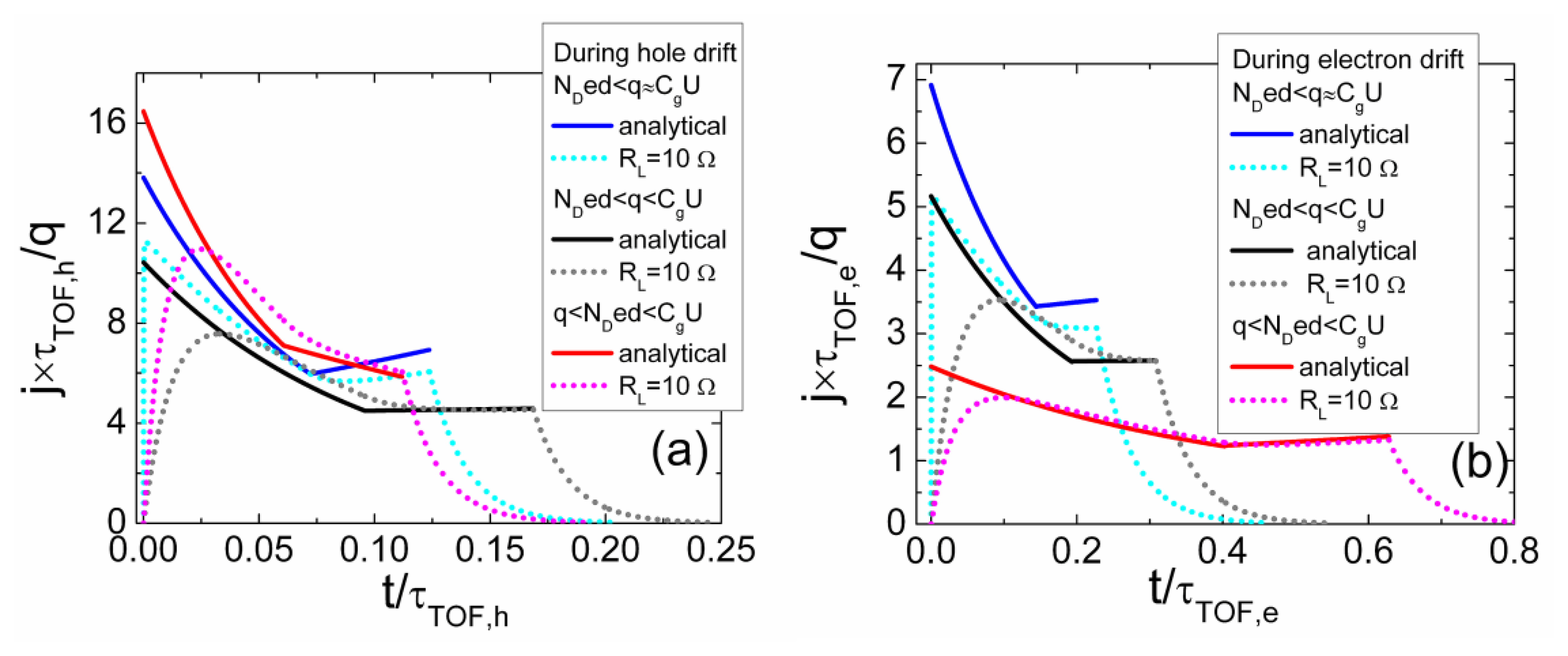
The simulated specific transient shapes associated with different regimes of the injected charge drift are illustrated in Figures 3 and 4. These simulations have been performed by using the above presented models and keeping nearly the same charge drift conditions, while varying external voltage to implement the partial or full depletion regimes. The described analytical solutions enable ones to get the continuous curves of the drifting charge velocity and of current density as a function of a domain position and of time. These illustrations demonstrate that current density transients, containing a rather flat pulse vertex, can be found in experiments implemented for the small injected charge density by using a small load resistance. However, only the largest current components can be resolved due to a weak signal. The double peak containing current transient shape should be observed as usual in the case of the relative large charge drift, Ramo's type, regime. Thereby, depending on the applied load resistor and voltage, a vast variety of current transient shapes can be obtained in modelling of detector responses.
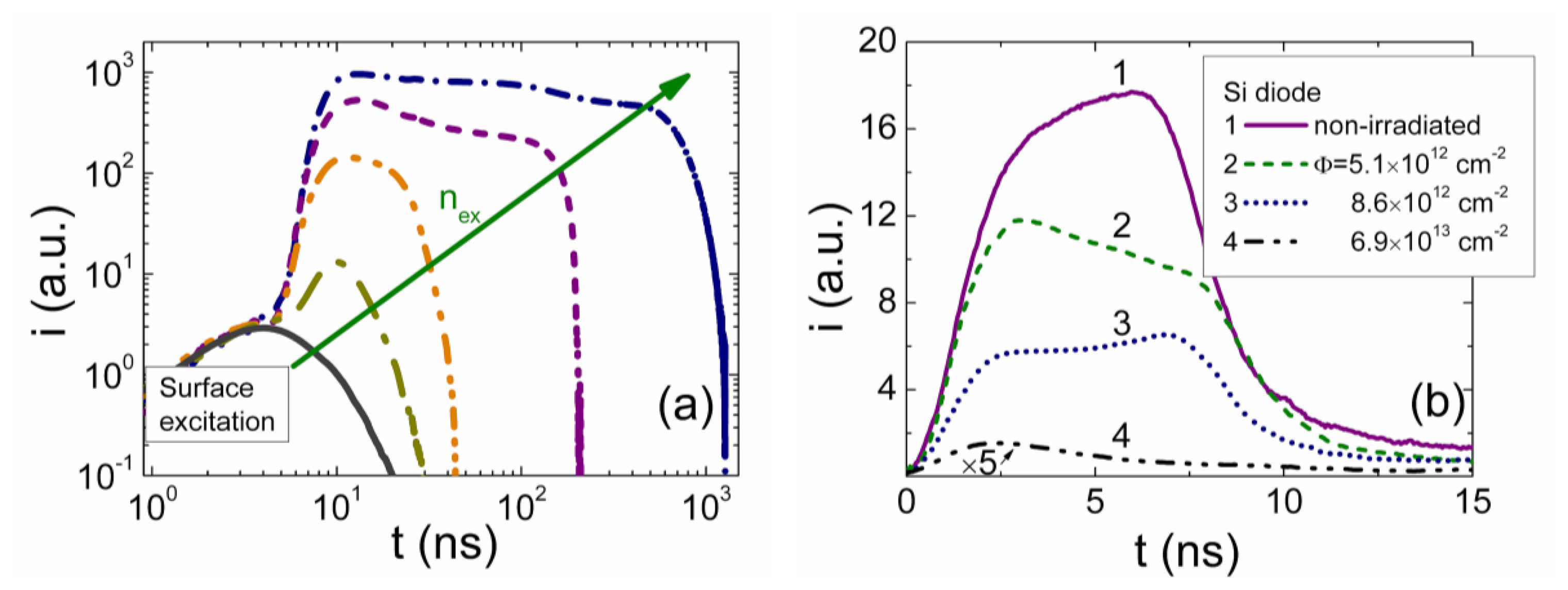
Variations of current transients due to the injected charge drift, observed in experiments, are illustrated in Figures 5. These variations are demonstrated as a function of the injected charge density, in Figure 5a. These transients were recorded on the non-irradiated CERN standard pad-detectors, made of pure Si of 2 kΩ cm resistivity p+nn+ structures. The reverse bias voltage was kept fixed with the rather moderate values U < UFD. The surface domain was injected by strongly absorbed light laser pulse of 400 ps duration. Density of the injected domain of electrons, initially located nearby a junction boundary, was varied by changing intensity of excitation laser beam. The laser pulse was sufficiently shorter than RC ≅ 1 ns of the measurement system. The pulsed current was detected on 50 Ω load resistor and registered by a 1 GHz band real time digital oscilloscope.
The transients, —characteristic to the pulse durations controlled by the ambipolar diffusion lifetime, are illustrated in Figure 5a using a logarithmic time scale. Here, the pulse duration is varied in the time scale from a few of nanosecond, —that is inherent for the electrons drift time in the base region, to a few microsecond of the diffusion time. It can be easily noticed that current increases with time within a vertex of a pulse for the smallest injected charge densities, as predicted by models described. The current pulse has nearly exponential relaxation component, after domain reaches the rear electrode. Duration of the pulse vertex, measured between the initial (which is on the left in this scale) and rearward kinks within current transient is well correlated with electron drift time in d = 300 μm thick Si layer, using μe ≅ 1,220 cm2/Vs value of the electron mobility. The enhancement of the injected charge density, proportional to the nex0 injected carrier concentration, leads to the increasing delay (of the rear kink in current transient) and to an increase of the current (proportional to qe), approaching to the ambipolar diffusion lifetime τD = d2/π2Da, ascribed to the main decay mode. The extracted value of the Da ≅ 15 cm2/s using the measured τD time is in good agreement with parameters ascribed to a rather pure Si material.
Variation of current transients measured at extremely small excitation densities (close to those possible to detect at a threshold sensitivity of the measurement system equipped with proper current amplifier) is illustrated in Figure 5b. These transients were recorded during 25 MeV neutron irradiation when density of radiation induced traps varied with neutrons fluence. The electrical (Ur = 150V) and optical (nex0) parameters were carefully controlled to be fixed within measurements. The sample was kept in air just behind the neutron beam cone, while other experiment details are published in [14,28]. Evolution of the current transients is illustrated in Figure 5b, where currents had been controlled starting from that registered in the non-irradiated diode up to exposure duration for which the collected irradiation fluence reaches value of > 1014 n/cm2. The transient waveform inherent to the drift dominated current (curve 1 in Figure 5b) is observed in the non-irradiated diode, which is coincident with modelled transient shape. The radiation introduced traps determine a rapid reduction of carrier lifetime and an enhancement of carrier capture and generation current components. The transient of the carrier capture dominated current contains the single peak, and the relaxation-type curve occurs (curve 4 in Figure 5b). In the range of the intermediate exposure time (curves 2 and 3 in Figure 5b), the current pulse duration sustains values of the electron drift time within a diode base. The double peak and rising pulse vertex shapes alternate during increase of fluence. Applying of the smallest possible densities of the surface charge was sufficient to hide the inhomogeneities of the photo-generated domain. This evolution of current transients can be explained by the competition of carrier capture/generation and drift currents. For the largest irradiation fluence, the carrier trapping process becomes dominant, while a drift current component is completely competed, and the relaxation-type current pulse is only observed.
7. Summary
The models of the formation of the injected charge pulsed currents have been developed concerning the junction-type detectors. The partial and full depletion regimes have been analyzed. It has been shown, that, in junction detector, the drift time for the rather small density of the injected charge is shortened relatively to that of the capacitor-like detectors when a proper frame of reference (for comparison) is accepted and the characteristic relaxation times are matched. The description of the current pulse shape for the large injected charge drift in a finite area detector is coincident with that derived for the correlated drift (Ramo's-type) expressions. However, the induced currents obtained for the regimes of the small injected charge and of partial depletion lead to deviations from the Ramo's expressions. The analysis of the drift velocity field revealed the current increase within a vertex of the current pulse, for the monopolar drift regime. It has been shown, that presence of carrier traps considerably modifies the shape of the current transients. For the extremely large density of the injected charge q > CgU, the ambipolar diffusion of the injected carriers may become dominant in formation of the injected charge current pulse. It has been illustrated, that synchronous action of carrier drift, trapping, generation and diffusion lead to a vast variety of possible current pulse waveforms. Experimental illustrations of the current waveform variations obtained for both the rather small and the large charge density of the photo-injected domains are presented, based on study of Si detectors.
Acknowledgments
This study was funded by the European Social Fund under the Global Grant measure project VP1-3.1-ŠMM-07-K-03-010.
Conflicts of Interest
The authors declare no conflict of interest.
References
- Ramo, S. Currents induced by electron motion. Proc. Inst. Radio Eng. 1939, 27, 584–585. [Google Scholar]
- Shockley, A. Currents to conductors induced by a moving point charge. J. Appl. Phys. 1938, 9, 635–636. [Google Scholar]
- Goulding, F.S. Semiconductor detectors for nuclear spectrometry, I. Nucl. Instrum. Meth. 1966, 43, 1–54. [Google Scholar]
- Martini, M.; Ottaviani, G. Ramo's theorem and the energy balance equations in evaluating the current pulse from semiconductor detectors. Nucl. Instrum. Meth. 1969, 67, 177–178. [Google Scholar]
- Vass, D.G. The charge collection process in semiconductor radiation detectors. Nucl. Instrum. Meth. 1970, 86, 5–11. [Google Scholar]
- Cavalleri, G.; Gatti, E.; Fabri, G.; Svelto, S. Extension of Ramo's theorem as applied to induced charge in semiconductor detectors. Nucl. Instrum. Meth. 1971, 92, 137–140. [Google Scholar]
- De Visschere, P. The validity of Ramo's theorem. Solid State Electron. 1971, 33, 455–459. [Google Scholar]
- Hamel, L.A.; Julien, M. Generalized demonstration of Ramo's theorem with space charge and polarization effects. Nucl. Instrum. Method. Phys. Res. A 2008, 597, 207–211. [Google Scholar]
- Kotov, I.V. Currents induced by charges moving in semiconductor. Nucl. Instrum. Method. Phys. Res. A 2005, 539, 267–267. [Google Scholar]
- Gatti, E.; Geraci, A. Considerations about Ramo's theorem extension to conductor media with variable dielectric constant. Nucl. Instrum. Method. Phys. Res. A 2004, 525, 623–625. [Google Scholar]
- Eremin, V.; Strokan, N.; Verbitskaya, E.; Li, Z. Development of transient current and charge techniques for the measurement of effective net concentration of ionized charges (Neff) in the space charge region of p-n junction detectors. Nucl. Instrum. Method. Phys. Res. A 1996, 372, 388–398. [Google Scholar]
- Leroy, C.; Roy, P.; Casse, G.; Glaser, M.; Grigoriev, E.; Lemeilleur, F. Study of charge transport in non-irradiated and irradiated silicon detectors. Nucl. Instrum. Method. Phys. Res. A 1999, 426, 99–108. [Google Scholar]
- Härkönen, J.; Eremin, V.; Verbitskaya, E.; Czellar, S.; Pusa, P.; Li, Z.; Niinikoski, T.O. The cryogenic transient current technique (C-TCT) measurement setup of CERN RD39 Collaboration. Nucl. Instrum. Method. Phys. Res. A 2007, 581, 347–350. [Google Scholar]
- Gaubas, E.; Ceponis, T.; Vaitkus, J.; Raisanen, J. Carrier drift and diffusion characteristics of Si particle detectors measured in situ during 8 MeV protons irradiation. Lith. J. Phys. 2011, 51, 351–358. [Google Scholar]
- Blood, P.; Orton, J.W. The Electrical Characterization of Semiconductors: Majority Carriers and Electron States; Academic Press: London, UK, 1992. [Google Scholar]
- WolframAlpha. Available online: http://www.wolframalpha.com (accessed on 25 July 2013).
- Kamke, E. Differrentialgleichungen. I-Gevonliche Differrentialgleichungen (Handbook); Akademische Verlagsgesellschaft Geest & Portig: Leipzig, Deutsche Demokratische Republik, 1959. [Google Scholar]
- Gaubas, E.; Ceponis, T.; Vaitkus, J.; Raisanen, J. Study of cariations of the carrier recombination and charge transport parameters during proton irradiation of silicon pin diode structures. AIP Adv. 2011, 1, 022143:1–022143:13. [Google Scholar]
- Bonch-Bruyevich, V.L.; Kalashnikov, S.G. Semiconductor Physics (In Russian); Nauka: Moscow, Russia, 1977. [Google Scholar]
- Gaubas, E.; Vaitkus, J.; Simoen, E.; Claeys, C.; Vanhellemont, J. Excess carrier cross-sectional technique for determination of the surface recombination velocity. Mater. Sci. Semicond. Process 2001, 4, 125–131. [Google Scholar]
- Gaubas, E. Transient absorption techniques for investigation of recombination properties in semiconductor materials. Lith. J. Phys. 2003, 43, 145–165. [Google Scholar]
- Luke, K.L.; Cheng, L.-J. Analysis of the interaction of a laser pulse with a silicon wafer: determination of bulk lifetime and surface recombination velocity. J. Appl. Phys. 1987, 61, 2282–2293. [Google Scholar]
- Spieler, H. Semiconductor Detector Systems; Oxford University Press: NY, USA, 2005. [Google Scholar]
- Lutz, G. Semiconductor Radiation Detectors—Device Physics; Springer: Heidelberg, Germany, 2007. [Google Scholar]
- Baliga, B.Y. Power Semiconductor Devices; PWS Publishing Company: MA, USA, 1995. [Google Scholar]
- Mott, N.F.; Gurney, R.W. Electronic Processes in Ionic Crystals, 2nd ed.; Dover Publications: NY, USA, 1964. [Google Scholar]
- Lampert, M. A.; Mark, P. Current Injection in Solids; Academic Press: NY, USA, 1970. [Google Scholar]
- Gaubas, E.; Ceponis, T.; Jasiunas, A.; Uleckas, A.; Vaitkus, J.; Cortina, E.; Militaru, O. Correlated evolution of barrier capacitance charging, generation and drift currents and of carrier lifetime in Si structures during 25 MeV neutron irradiation. Appl. Phys. Lett. 2012, 101, 232104:1–232104:3. [Google Scholar]


© 2013 by the authors; licensee MDPI, Basel, Switzerland. This article is an open access article distributed under the terms and conditions of the Creative Commons Attribution license (http://creativecommons.org/licenses/by/3.0/).
Share and Cite
Gaubas, E.; Ceponis, T.; Kalesinskas, V. Currents Induced by Injected Charge in Junction Detectors. Sensors 2013, 13, 12295-12328. https://doi.org/10.3390/s130912295
Gaubas E, Ceponis T, Kalesinskas V. Currents Induced by Injected Charge in Junction Detectors. Sensors. 2013; 13(9):12295-12328. https://doi.org/10.3390/s130912295
Chicago/Turabian StyleGaubas, Eugenijus, Tomas Ceponis, and Vidas Kalesinskas. 2013. "Currents Induced by Injected Charge in Junction Detectors" Sensors 13, no. 9: 12295-12328. https://doi.org/10.3390/s130912295