Focal-Plane Sensing-Processing: A Power-Efficient Approach for the Implementation of Privacy-Aware Networked Visual Sensors


 ,
, 

Abstract
: The capture, processing and distribution of visual information is one of the major challenges for the paradigm of the Internet of Things. Privacy emerges as a fundamental barrier to overcome. The idea of networked image sensors pervasively collecting data generates social rejection in the face of sensitive information being tampered by hackers or misused by legitimate users. Power consumption also constitutes a crucial aspect. Images contain a massive amount of data to be processed under strict timing requirements, demanding high-performance vision systems. In this paper, we describe a hardware-based strategy to concurrently address these two key issues. By conveying processing capabilities to the focal plane in addition to sensing, we can implement privacy protection measures just at the point where sensitive data are generated. Furthermore, such measures can be tailored for efficiently reducing the computational load of subsequent processing stages. As a proof of concept, a full-custom QVGA vision sensor chip is presented. It incorporates a mixed-signal focal-plane sensing-processing array providing programmable pixelation of multiple image regions in parallel. In addition to this functionality, the sensor exploits reconfigurability to implement other processing primitives, namely block-wise dynamic range adaptation, integral image computation and multi-resolution filtering. The proposed circuitry is also suitable to build a granular space, becoming the raw material for subsequent feature extraction and recognition of categorized objects.1. Introduction
The Internet-of-Things (IoT) paradigm envisions an addressable continuum of interconnected smart objects exchanging information via the Internet [1]. One of the major objectives for this paradigm is minimum human intervention, targeting autonomous devices seamlessly integrated in our daily lives without explicit instructions [2]. In this context, sensor networks arise as an essential component of the IoT [3]. They take on the task of collecting data from the physical world, leading to the eventual activation of the actuators that carry out the decided actions. In terms of the measurements taken by the sensors, we can distinguish between scalar and non-scalar magnitudes. Scalar magnitudes, like temperature, pressure or humidity, have traditionally defined the application domains of sensor networks, e.g., precision agriculture [4], structural health [5] or meteorological analysis [6]. However, ongoing advances in electronics, sensor technologies, embedded hardware and software are enabling the incorporation of non-scalar magnitudes into the catalog of sensing capabilities of these networks. Specifically, the incorporation of vision means a challenge due to the strong restrictions imposed by the scarcity of resources—power, processing and memory—at the network nodes [7].
Before dealing with demanding low-level system requirements, a critical issue at the highest abstraction level must be carefully addressed first: privacy. Pervasive surveillance by networked image sensors creates legal and societal concerns. Citizens' sensitive information can be put at risk, causing people to reject the technology. Fortunately, identifiable personal data—faces, clothes, wearables etc.—are usually not needed to perform meaningful visual analysis in prospective application scenarios of visual sensor networks like retail analytics, factory monitoring or elderly care. Time spent by customers in front of a showcase, trajectories of workers around a manufacturing site or fall detection in a nursing home are three examples where video analytics can be realized without compromising privacy by discarding identifiable information early on. However, the concerns are understandably still there, because current smart imaging systems rely on a significant number of key software components to prevent leaking sensitive information. The implicitly trusted software base includes the operating system, the network stack, system libraries, etc. It is not possible to provide complete assurance about the potential security and privacy flaws contained in this software [8]. Even widely adopted cryptography libraries are not free of such flaws [9]. A possible approach to overcome these limitations is to convey protection as close to the sensing device as possible. In this regard, the system architecture presented in [10] constitutes state-of-the-art work related to privacy protection in camera networks. A strong separation between specific camera modules—hardware and software—accessing sensitive raw data and those ones devoted to application tasks is proposed. While this approach features a good tradeoff between security and system flexibility, there is still a number of trusted software components involved in the operation of the secure sensing unit. The ideal framework would be a front-end vision sensor delivering a data flow stripped of sensitive information. On-chip implementation of such stripping would still have to accommodate some degree of reconfigurability in order to balance protection and viability of the video analytics required by particular algorithms. Once protection measures are embedded on-chip at the front-end sensor of each network node, the number of trusted components as well as the impact of potential software flaws are significantly reduced.
Despite the importance of privacy for boosting the adoption of visual sensor networks, most prototype image sensors tailored for saving node resources do not address any protection measures in this respect [11–14]. Monolithic “light-in answer-out” system-on-a-chip solutions have been reported [15]. In this case, the sensor includes a small array of photo-diodes capturing 128 × 128-px images that feed an on-chip pipeline processing architecture. Images are never delivered off-chip. Extremely high performance is accomplished, but at the cost of low resolution and complex hardwired program control patterns. No alternative is considered either for applications requiring external storage of obfuscated images. Another privacy-aware approach for sensor networks is address-event representation (AER) [16]. Instead of full-resolution images, AER-based sensors constrain their outputs to codified events triggered by specific features like motion, light saturation or spatio-temporal contrast. The inherent filtering process of their operation removes sensitive data, but also most of the scene details, significantly reducing the scope of the video analytics applicable.
In this paper, we present a low-power vision sensor aiming at balancing processing flexibility and privacy protection. Sensitive image regions can be obfuscated through tunable pixelation at the focal plane. This tuning permits to preserve detailed image information if needed. The reconfiguration of the chip to dynamically accommodate vision algorithm requirements takes place on-the-fly. Other low-level processing primitives, like block-wise high dynamic range (HDR), integral image computation and multi-resolution filtering, can also be implemented by the prototype, boosting its scope of application. Plentiful experimental results are provided. Finally, the proposed sensing-processing scheme is also suitable to build a granular space [17] by exploiting focal-plane distributed memory. This granular space constitutes the raw material for subsequent recognition of categorized objects. It can also be adjusted, if afforded by the targeted application, to operate with coarse enough granule scales for the sake of privacy. In such a case, we would be concurrently combining purposeful power-efficient focal-plane processing and privacy protection.
2. Focal-Plane Sensing-Processing
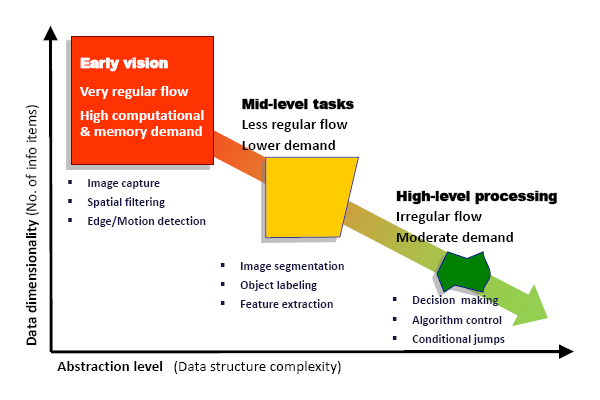
Artificial vision, understood as the process of automatically extracting meaningful information from visual stimulus, is usually divided into three consecutive stages: early vision, mid-level tasks and high-level processing [18]. If we compare these stages in terms of data dimensionality, i.e., the number of information items versus the abstraction level, that is, the complexity of the data, a chart like that of Figure 1 can be depicted. Early vision operates on each and every pixel resulting from the raw readings of the sensor, but features a very regular computational flow: the same calculations are repeatedly carried out on every pixel. Mid-level tasks do not operate on raw data, but on a smaller amount of information of a higher abstraction level. Finally, high-level processing, of a cognitive nature, provides the semantic interpretation of the scene. It operates on a very reduced amount of data under a very irregular instruction flow. From this global picture of the vision process, we can conclude that early vision represents the critical stage in terms of computational and memory demands.
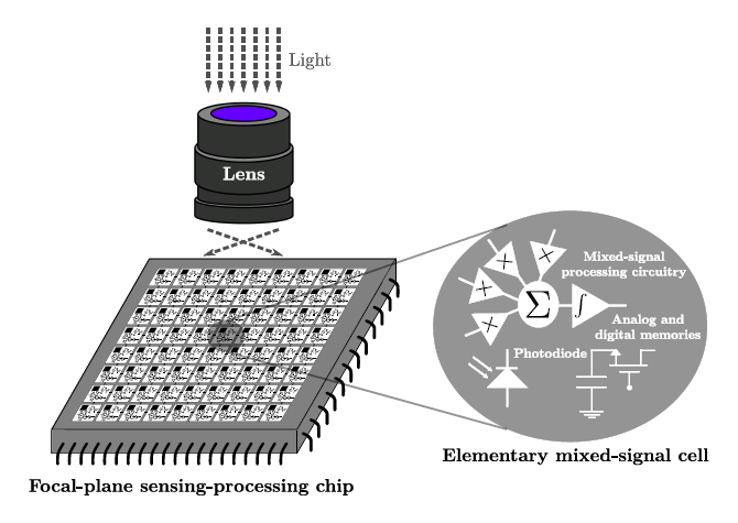
Focal-plane sensing-processing [19] is arguably the best architectural approach reported concerning adaptation to the particular characteristics of early vision. It is inspired in the operation of natural vision systems where a front-end device, the retina, does not only acquire, but also pre-processes the visual information. As a result of this pre-processing, the amount of data transmitted through the optic nerve to the brain gets compressed by a factor of ∼100 [20]. Different simplified representations of the scene being observed are rendered at this stage, speeding up its interpretation by the visual cortex. Focal-plane sensor-processor chips mimic this processing arrangement, as shown in a simplified way in Figure 2. An array of interconnected elementary mixed-signal cells, also known as multi-functional pixels, plays the role of front-end device in this case. The array usually operates in single-instruction multiple-data (SIMD) mode featuring concurrent processing and distributed memory. Focal-plane architectures can also benefit from incorporating analog circuitry just at the point where the analog data feeding the processing chain are sensed. These analog circuits can reach higher performance in terms of speed, area and power consumption than digital circuitry while exploiting the moderate accuracy requirements of early vision tasks. Numerous low-level image processing primitives have been successfully implemented following this scheme: convolution filtering [21,22], programmable blurring [23], spatial [24] and temporal [25] contrast extraction, background subtraction [26], image compression [27] or high dynamic range imaging [28], among others. Even academic [29] and commercial [30] general-purpose vision systems based on focal-plane processing have been reported.
3. A QVGA Focal-Plane Sensor-Processor Chip with Multi-Functional Pixels
3.1. Chip Architecture
The concept of focal-plane sensing-processing just described arises as the best framework to explore privacy protection for visual sensor networks. First of all, hackers will find it extremely difficult to tap sensitive information obfuscated from the very point where it is captured. Second, our ultimate objective is the implementation of a low-power high-performance vision system suitable for the scarce resources available at network nodes. In this regard, focal-plane sensing-processing features an architecture adapted for the efficient exploitation of the inherent properties of vision.
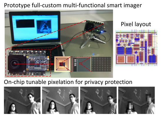
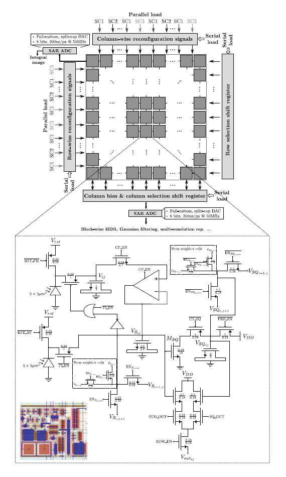
All in all, the proposed prototype vision sensor presents the floor plan depicted in Figure 3. An array of four-connected mixed-signal multi-functional pixels constitutes its operative core. This array can be reconfigured block-wise by peripheral circuitry. The reconfiguration patterns are loaded serially into two shift registers that determine respectively which neighbor columns and rows can interact and which ones stay disconnected. There is also the possibility of loading in parallel up to six different patterns representing six successive image pixelation scales. This is achieved by means of control signals distributed regularly along the horizontal and vertical dimensions of the array [31]. The reconfiguration signals coming from the periphery map into the signals ENSi,i+1, ENSj,j+1, and at pixel level, where the coordinates (i,j) denote the location of the array cell considered. These signals control the activation of MOS switches for charge redistribution between the nMOS capacitors holding the voltages VSij and VSQij, respectively. Charge redistribution is the primary processing task that supports all of the functionalities of the array, enabling a low-power operation. Concerning A-to-D conversion, there are four eight-bit SAR ADCs. These converters, based on a split-cap DAC, feature a tunable conversion range, including rail-to-rail, and a conversion time of 200 ns when clocked at 50 MHz. Two of them provide integral imaging. The other two convert the pixel voltage Voutij corresponding to the selected output of the source followers associated with VSij and VQij. The column and row selection circuitry is also implemented by peripheral shift registers where a single logic “1” is shifted according to the location of the pixel to be converted. The power consumption of the chip ranges from 42.6 mW for high dynamic range operation to 55.2 mW for integral image computation at 30 fps. It has been fabricated in a standard 0.18 μm CMOS process. The main characteristics of the chip are summarized in Table 1. A comparison with state-of-the-art focal-plane sensor-processor chips is presented in Table 2. Our prototype embeds the greatest functionality while featuring the largest resolution and the smallest pixel pitch, with a cost in terms of reduced fill factor.
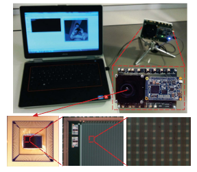
For test purposes, the vision sensor has been embedded into a system based on the commercial FPGA-based DE0-Nano board from terasIC. The operation of the chip is fully controlled through 85 digital signals and 21 analog signals, thus enabling its integration with high-level power management schemes [35,36] in order to set low-power operation and idle states. The test system, together with some microphotographs of the chip, can be seen in Figure 4. The output data flow provided by the sensor is stored in the internal memory of the FPGA for its subsequent serial transmission to a PC through a USB interface. The data rearrangement and image visualization in the PC are implemented by making use of OpenCV functionalities.
3.2. On-Chip Early Vision
3.2.1. Privacy Protection through Programmable Pixelation
Various techniques for privacy protection have been reported in the literature. The most basic form is blanking [37], where sensitive regions are completely removed from the captured images. No behavioral analysis is possible in this case; only the presence and location of a person can be monitored. Other alternatives that do enable such analysis are obfuscation and scrambling [38]. Concerning obfuscation, pixelation of sensitive regions provides the best performance in terms of balance between privacy protection and intelligibility of the surveyed scene when compared to blurring and masking filters [39,40]. New techniques for obfuscation, like warping [41] or cartooning [42], have been recently proposed.
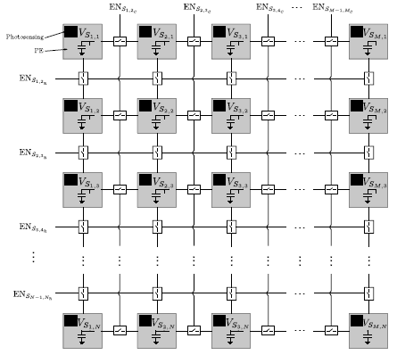
The on-chip programmable pixelation is achieved by combining focal-plane reconfigurability, charge redistribution and distributed memory. After photointegration, the corresponding pixel values are represented by the voltages Vij distributed across the array. These pixel values can be copied in parallel into the voltages VSij by enabling the analog buffer included at each elementary cell. This copy process takes about 150 ns for the whole array. It is not destructive with respect to the original voltages Vij, which is crucial to accomplish focal-plane obfuscation without artifacts, as explained below. Once the voltages VSij are set, the next step consists in establishing the adequate interconnection patterns according to the image regions to be pixelated and the required degree of obfuscation. These patterns, when activated by the corresponding control signal, will enable charge redistribution among the connected capacitors holding VSij, i.e., the image copy. Figure 5 shows a simplified scheme of how the charge redistribution can be reconfigured column-wise and row-wise from the periphery of the proposed focal-plane array. Every pair of neighboring columns and rows shares a common interconnection signal that is independent of the interconnection signals for any other pair. When the interconnections of consecutive columns and rows are enabled, voltage averaging, i.e., charge redistribution, will take place within the resulting block. Otherwise, the pixel values remain unchanged.
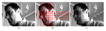
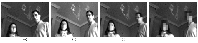
An example of the focal-plane obfuscation attainable by applying this operation is shown in Figure 6. The first snapshot represents an image captured by the chip. The interconnection patterns established ad hoc for the pixelation of the face in the scene are highlighted in the second picture. Finally, the third image depicts the resulting focal-plane representation. It can be seen that the existence of a single control signal for the interconnection of all of the cells along particular neighbor columns and rows generates spurious blocks within which partial charge redistribution also occurs. The consequent artifacts significantly reduce the amount of useful information contained in the image, distorting its content. However, we can overcome this problem by exploiting the distributed memory inherent to the sensing-processing array. Bear in mind that the image in Figure 6c is the outcome after photointegration, pixel copy, interconnection setting, charge redistribution and A-to-D conversion. This last stage is key to remove the aforementioned artifacts. During A-to-D conversion, we copy the corresponding original pixel value still stored in the capacitors holding Vij for the regions where full resolution is affordable in terms of privacy. Otherwise, averaging is allowed. On-chip obfuscation without artifacts can thus be achieved, as shown in Figure 7. In this case, we set interconnection patterns for progressively coarser simultaneous pixelation of two different image regions containing faces.
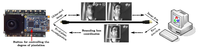
Finally, as an example of on-the-fly focal-plane reconfiguration conducted by a vision algorithm, we set up a closed loop between our test system and the Viola-Jones frontal face detector provided by OpenCV, as depicted in Figure 8. The sensor captures images that are sent to a PC from the test board. The Viola-Jones detector is run on these images on the PC. If faces are detected, the coordinates of the corresponding bounding rectangles are sent back to the test board for the vision sensor to reconfigure the image capture in real time. Pixelation of the face regions will take place from that moment on at the focal plane. The degree of pixelation of these regions is adjustable through a button of the test board. A sequence extracted during the execution of this loop can be download from [43]. Notice that all of the reconfiguration and control of the array must be carried out externally for this prototype. The FPGA of the DE0-Nano board plays such a role in the test system.
3.2.2. Block-Wise HDR
One of the fundamental problems that visual sensors have to cope with is the inspection of scenes featuring a wide range of illuminations. In such cases, assuming the usual photocurrent integration mode, the application of the same exposure time across the pixel array leads to either over-exposed or under-exposed regions. The consequent low contrast and missing details can make the processing of these regions unfeasible. The processing primitive described next is specially suitable for vision algorithms requiring tracking of regions of interest (ROI) [44,45] in such circumstances.
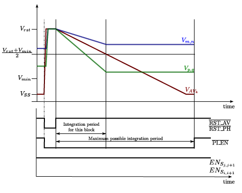
The two photodiodes and two sensing capacitances included at the elementary cell in Figure 3 are required to implement this low-level operation. Their reset to the voltage Vrst, which coincides with the upper limit of the signal range, is controlled through the signals , and . When the three of them are set to logic “0”, the reset of the so-called pixel photodiode, averaging photodiode and averaging capacitance is immediately enabled. If the voltage VSij starts from a value above the input threshold voltage of the inverter, Vthinv, the reset of the pixel capacitance holding Vij is concurrently initiated. Otherwise, as is the case in the illustrating timing diagram of Figure 9, this reset will be delayed slightly until VSij reaches that threshold. A key aspect of the circuit is that the inverter must be designed in such a way that Vthinv is located just at the middle point of the signal range, that is:
An example of this operation is shown in Figure 10. Global control of the integration time is applied to the left image. All pixels undergo the same integration time, which is set to 500 ms according to the mean illumination of the scene. Details about the lamp are missed due to the extreme deviation with respect to this mean illumination. However, such details can be retrieved by confining the control of the integration period to the region of interest, as can be seen in the right image. In this case, the integration time of the region around the center of the lamp adjusts locally and asynchronously to its mean illumination, stopping the photointegration at around 400 μs in that particular area while it continues at the remaining regions.
3.2.3. Integral Image
The so-called integral image is a common intermediate image representation used by well-known vision algorithms, e.g., the Viola–Jones framework for object detection [47]. It is defined as:
The array can also compute an averaged version of the square integral image. To this end, we make use of the squarer experimentally tested and reported in [48]. Thus, by precharging the capacitor holding VSQij to VDD and exploiting its discharge for a short period of time through the transistor MSQ working in the saturation region, the value of the pixel square can be computed. Then, charge redistribution takes over, just as for the integral image. Indeed, apart from the required previous computation of the pixel square, the procedure to obtain the averaged versions of the integral image and the square integral image is exactly the same, applied respectively to the voltages VSij and VSQij at the pixel level. A timing diagram showing two consecutive computations of integral image pixels is depicted in Figure 11. In order to read out and convert these pixels, we must simply connect VS1,1 and VSQ1,1 to the respective analog-to-digital converters. These voltages will always contain the targeted calculation for each pixel, according to the definition of integral image and the proposed hardware implementation based on charge redistribution.
An example of on-chip integral image computation is shown in Figure 12. In this case, we can visualize the averaged integral image delivered by the chip and the integral image that can be directly derived from it. This integral image is compared to the ideal integral image obtained off-chip with MATLAB from the original image captured by the sensor, attaining an RMSE of 1.62%.
3.2.4. Multi-Resolution Filtering
The combination of focal-plane reconfigurability, charge redistribution and distributed memory enables subsequent reduced kernel filtering by adjusting which pixels merge their values and in which order. Very useful image filtering kernels, like the binomial filter mask for image Gaussian smoothing or the Sobel operators for edge detection, fall into the category of reducible kernels [49]. Operating on the pre-processed image with one of them represents a smaller number of operations per pixel than realizing all of the multiply-accumulate operations needed to apply the corresponding original kernels. Memory accesses are reduced in the same fraction. An example of Gaussian filtering is depicted in Figure 13.
4. Guidelines for Future Work: Feature Extraction from On-Chip Granular Space
This section describes how the proposed on-chip reconfiguration scheme can be adapted to speed up object recognition and even to concurrently combine this task with privacy protection. Note that our sensor was not designed with this application in mind. The connection between the different concepts involved came later when exploring image features suitable for our focal-plane sensing-processing approach. Therefore, key parameters of the prototype have not been tuned for reaching real-time operation in this case. Nevertheless, we consider that the hardware-software co-design framework sketched next is a completely new idea in the field of embedded vision systems. It will constitute a solid base supporting the process of setting specifications for a future sensor chip.
4.1. Granular Space
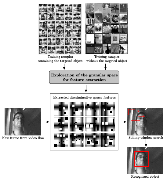
There are two major approaches for generic object recognition in computer vision: window-based object representations and part-based object representations [50]. Window-based representations perform better for recognition of rigid objects with a certain regularity in their spatial layout. They implement a holistic description of appearance based on a dense sampling of features obtained at multiple scales. To determine the presence or absence of a certain object in a new image, this approach makes use of a sliding window testing all possible sub-windows of the image with a previously trained classifier. On the other hand, part-based representations usually perform better for non-rigid deformable objects, since these describe the appearance of an object through local parts following a certain geometric interconnection pattern. They therefore incorporate more detailed spatial relations into the recognition procedure, requiring complex search procedures for the detection of image keypoints. Conversely, they require fewer training examples. Generally speaking, it has been observed that, given sufficient training data, the discriminative sliding-window models outperform when it comes to recognizing typical targeted objects for embedded vision like faces or front/back views of pedestrians.
The so-called granular space for feature extraction belongs to the sliding-window category. It was first defined in [17], being applied for multi-view face detection. It simply consists in a multi-resolution space composed of the so-called granules that observe each image instance at different locations and scales. The granules are represented by the average value of their constituting pixels. By combining different granules across the image, a new sparse feature is obtained. A large number of these sparse features are learned during training for a particular object. They are later analyzed during real operation for new images where such an object could be present. A scheme of the procedure is depicted in Figure 14. The white and black granules are respectively weighted positively and negatively when it comes to attaining a representative value of the corresponding sparse feature. This value is then compared with that of another feature or with a threshold, according to the classification technique applied.
The original work in [17] has been extended during the last few years mostly by introducing variations in the training and feature search strategy [51–54]. The recognition of other objects, like pedestrians, has also been addressed. Still, the raw material feeding the whole processing chain keeps being the granular space. It is on building this space where focal-plane sensing-processing can contribute to boosting the global performance.
4.2. On-Chip Processing
The granular space is ultimately based on block-wise averaging across the image plane. Coincidentally, the operation of averaging, physically supported by charge redistribution, is one of the most efficient computations to be realized in parallel at the focal plane. As we described in Section 3.2.1, we have successfully implemented a focal-plane reconfiguration scheme for block-wise programmable averaging in our prototype vision chip. This scheme permits to apply division grids enabling the concurrent computation of rectangular-shaped granules of any size across the whole image, as depicted in Figure 15. For the grids of this example, the focal-plane array required only ∼200 ns to respectively calculate 300, 2400 and 1220 granules in parallel. Unfortunately, the bottleneck for real-time operation arises during the A/D conversion. As mentioned earlier, the chip was not designed to provide several scales of the granular space per frame in real time as would be required by an algorithm of object recognition based on sparse feature extraction in such a space. Specifically, we should have included additional in-pixel memory and additional A/D converters working in parallel according to the targeted frame rate and number of scales. Finally, notice that the computation of granules at the focal plane, while meaningful from the perspective of object recognition, implies a significant distortion of the image content. Such a distortion can be exploited for privacy protection as long as the subsequent classifier can afford to work with granules of a large enough minimum size.
4.3. Hardware-Software Co-Design Framework
A great deal of tradeoffs affecting both hardware and software will have to be considered for the design and implementation of a future network visual node based on the focal-plane generation of the granular space. Key parameters for the performance of such a node, like the resolution, the frame rate or the detection rate, must be determined by carefully adjusting design variables, like the pixel size, sensitivity or conversion time (hardware level), together with others, like the size of the granules or the training technique (software level). From our point of view, software simulations must first set the initial tentative specifications for the hardware. To this end, we are starting to build a tunable classifier based on features extracted from the granular space. The design loop will be closed by hardware simulations derived from the initial specifications provided by the classifier. These simulations will then feedback software simulations and vice versa in a constant process of parameter adjustment and performance evaluation. Eventually, we will obtain accurate requirements for a smart imager tailored for a privacy-aware vision system providing reliable object recognition at low power consumption.
5. Conclusions
The deployment of ubiquitous networked visual sensors seamlessly integrated in the Internet of Things is still a challenge to be accomplished. Privacy and power consumption are two major barriers to overcome. Once visual information is disconnected from private data and locally processed by low-power trusted computing devices, a wide range of innovative applications and services will be able to be addressed; applications and services now impossible to be implemented because current technology collides with legal constraints and public rejection. The ultimate objective is that such vision-enabled devices represent a concern not higher than lighting or door control based on automatic presence detectors. In this paper, we have reported our contribution to advance the state of the art regarding privacy and ultra-low-power in-node processing for visual sensor networks. A full-custom prototype vision sensor has been presented. Its most distinctive feature, in addition to power efficiency, is the reconfigurability of its focal-plane sensing-processing array. This reconfigurability enables real-time adaptation to specific requirements from vision algorithms. Particularly, we have demonstrated that concurrent obfuscation of different image regions can be achieved directly at the focal-plane. A new framework for merging focal-plane privacy protection and purposeful parallel processing has also been sketched. This framework, based on the extraction of sparse features from the granular space, will be our research focus in the short/mid-term.
Acknowledgments
This work has been funded by the Spanish Government through projects TEC2012-38921-C02 MINECO, MINisterio de Economía y COmpetitividad (European Region Development Fund, ERDF/FEDER), IPT-2011-1625-430000 MINECO and IPC-20111009 CDTI, Centro para el Desarrollo Tecnológico Industrial (ERDF/FEDER), Junta de Andalucía through project TIC 2338-2013 CEICE, Consejería de Economía, Innovación, Ciencia y Empleo, by the Office of Naval Research (USA) through Grant N000141410355 and by the Faculty of Engineering of Ghent University through its program for visiting foreign researchers.
Author Contributions
Jorge Fernández-Berni was the principal designer of the chip reported in this paper. Ricardo Carmona-Galán, Rocío del Río and Ángel Rodríguez-Vázquez also contributed crucially for its successful implementation. Richard Kleihorst and Wilfried Philips set the grounds for the interrelation between the prototype vision sensor and the feature extraction from the granular space.
Conflicts of Interest
The authors declare no conflict of interest.
References
- European Commision. Internet of Things in 2020, a Roadmap for the Future. RFID Working Group of the European Technology Platform on Smart Systems Integration, 2008. Available online: http://www.smart-systems-integration.org/public/internet-of-things (accessed on 11 June 2014).
- Dohr, A.; Modre-Osprian, R.; Drobics, M.; Hayn, D.; Schreier, G. The Internet of Things for ambient assisted living. Proceedings of the International Conference on Information Technology, Las Vegas, NE, USA, 12–14 April 2010; pp. 804–809.
- Perera, C.; Zaslavsky, A.; Christen, P.; Georgakopoulos, D. Context aware computing for the Internet of Things: A survey. IEEE Commun. Surv. Tutor. 2014, 16, 414–454. [Google Scholar]
- McCulloch, J.; McCarthy, P.; Guru, S.; Peng, W.; Hugo, D.; Terhorst, A. Wireless sensor network deployment for water use efficiency in irrigation. Proceedings of the Workshop on Real-World Wireless Sensor Networks (REALWSN), Glasgow, Scotland, 1–4 April 2008; pp. 46–50.
- Kim, S.; Pakzad, S.; Culler, D.; Demmel, J. Health Monitoring of Civil Infrastructures Using Wireless Sensor Networks. Proceedings of the International Conference on Information Processing in Sensor Networks (IPSN), Cambridge, MA, USA, 25–27 April 2007; pp. 254–263.
- Barrenetxea, G.; Ingelrest, F.; Schaefer, G.; Vetterli, M. The hitchhiker's guide to successful wireless sensor network deployments. Proceedings of the International Conference on Embedded Network Sensor Systems (SenSys), Raleigh, NC, USA, 4–7 November 2008; pp. 43–56.
- Bulent, T.; Bicakci, K.; Zilan, R.; Barcelo-Ordinas, J.M. A survey of visual sensor network platforms. Multimed. Tools Appl. 2012, 60, 689–726. [Google Scholar]
- Winkler, T.; Rinner, B. Sensor-level security and privacy protection by embedding video content analysis. Proceedings of the IEEE International Conference on Digital Signal Processing (DSP), Santorini, Greece, 1–3 July 2013; pp. 1–6.
- OpenSSL Project. Heartbeat Overflow Issue, 2014. Available online: https://www.openssl.org/news/secadv_20140407.txt (accessed on 11 June 2014).
- Winkler, T.; Erdélyi, Á.; Rinner, B. TrustEYE.M4: Protecting the sensor—Not the camera. Proceedings of the International Conference on Advanced Video and Signal-Based Surveillance (AVSS), Seoul, Korea, 26–29 August 2014.
- Zhang, G.; Ynag, T.; Gregori, S.; Liu, J.; Maloberti, F. Ultra-low power motion-triggered image sensor for distributed wireless sensor network. IEEE Sens. 2003, 2, 1141–1146. [Google Scholar]
- Fang, T.; Bermak, A. An 84 pW/Frame Per Pixel Current-Mode CMOS Image Sensor with Energy Harvesting Capability. IEEE Sens. 2012, 12, 720–726. [Google Scholar]
- Choi, J.; Park, S.; Cho, J.; Yoon, E. A 1.36 μW adaptive CMOS image sensor with reconfigurable modes of operation from available energy/illumination for distributed wireless sensor network. Proceedings of the IEEE International Solid-State Circuits Conference (ISSCC), San Francisco, CA, USA, 19–23 February 2012; pp. 112–114.
- Choi, J.; Park, S.; Cho, J.; Yoon, E. A 3.4 μW Object-Adaptive CMOS Image Sensor with Embedded Feature Extraction Algorithm for Motion-Triggered Object-of-Interest Imaging. IEEE J. Solid-State Circuits 2014, 49, 289–300. [Google Scholar]
- Cheng, C.-C.; Lin, C.-H.; Li, C.-T.; Chen, L.-G. iVisual: An Intelligent Visual Sensor SoC With 2790 fps CMOS Image Sensor and 205 GOPS/W Vision Processor. IEEE J. Solid-State Circuits 2009, 44, 127–135. [Google Scholar]
- Teixeira, T.; Culurciello, E.; Park, J.; Lymberopoulos, D.; Barton-Sweeney, A.; Savvides, A. Address-event imagers for sensor networks: Evaluation and modeling. Proceedings of the IEEE International Conference Information Processing in Sensor Networks (IPSN), Nashville, TN, USA, 19–21 April 2006; pp. 458–466.
- Huang, C.; Ai, H.; Li, Y.; Lao, S. Learning sparse features in granular space for multi-view face detection. Proceedings of the International Conference on Automatic Face and Gesture Recognition (FGR), Southampton, UK, 10–12 April 2006; pp. 401–406.
- Gonzalez, R.; Woods, R. Digital Image Processing; Prentice Hall: Upper Saddle River, NJ, USA, 2002. [Google Scholar]
- Zarándy, Á., Ed.; Focal-Plane Sensor-Processor Chips; Springer: Berlin, Germany, 2011.
- Roska, B.; Werblin, F. Vertical interactions across ten parallel, stacked representations in the mammalian retina. Nature 2001, 410, 583–587. [Google Scholar]
- Nilchi, A.; Aziz, J.; Genov, R. Focal-plane algorithmically-multiplying CMOS computational image sensor. IEEE J. Solid-State Circuits 2009, 44, 1829–1839. [Google Scholar]
- Jendernalik, W.; Blakiewicz, G.; Jakusz, J.; Szczepanski, S.; Piotrowski, R. An analog sub-miliwatt CMOS image sensor with pixel-level convolution processing. IEEE Trans. Circuits Syst. I 2013, 60, 279–289. [Google Scholar]
- Fernández-Berni, J.; Carmona-Galán, R. All-MOS implementation of RC networks for time-controlled Gaussian spatial filtering. Int. J. Circuit Theory Appl. 2012, 40, 859–876. [Google Scholar]
- Gottardi, M.; Massari, N.; Jawed, S. A 100 μW 128 × 64 pixels contrast-based asynchronous binary vision sensor for sensor networks applications. IEEE J. Solid-State Circuits 2009, 44, 1582–1592. [Google Scholar]
- Leñero-Bardallo, J.A.; Serrano-Gotarredona, T.; Linares-Barranco, B. A 3.6 μs Latency asynchronous frame-free event-driven dynamic-vision-sensor. IEEE J. Solid-State Circuits 2011, 46, 1443–1455. [Google Scholar]
- Cottini, N.; Gottardi, M.; Massari, N.; Passerone, R.; Smilansky, Z. A 33 μW 64 × 64 pixel vision sensor embedding robust dynamic background subtraction for event detection and scene interpretation. IEEE J. Solid-State Circuits 2013, 48, 850–863. [Google Scholar]
- Oliveira, F.; Haas, H.; Gomes, J.; Petraglia, A. CMOS imager with focal-plane analog image compression combining DPCM and VQ. IEEE Trans. Circuits Syst. I 2013, 60, 1331–1344. [Google Scholar]
- Messaoud, F.; Peizerat, A.; Dupret, A.; Blanchard, Y. On-chip compression for HDR image sensors. Proceedings of the Conference on Design and Architectures for Signal and Image Processing (DASIP), Madrid, Spain, 8–10 October 2010; pp. 176–182.
- Lopich, A.; Dudek, P. Asynchronous cellular logic network as a co-processor for a general-purpose massively parallel array. Int. J. Circuit Theory Appl. 2011, 39, 963–972. [Google Scholar]
- Rodríguez-Vázquez, A.; Domínguez-Castro, R.; Jímenez-Garrido, F.; Morillas, S.; Listán, J.; Alba, L.; Utrera, C.; Espejo, S.; Romay, R. The Eye-RIS CMOS vision system. In Sensors, Actuators and Power Drivers; Integrated Power Amplifiers from Wireline to RF; Very High Frequency Front Ends; Casier, H., Steyaert, M., Van Roermund, A., Eds.; Springer: Berlin, Germany, 2011; pp. 15–32. [Google Scholar]
- Fernández-Berni, J.; Carmona-Galán, R.; del Río, R.; Rodríguez-Vázquez, A. Bottom-up performance analysis of focal-plane mixed-signal hardware for Viola-Jones early vision tasks. Int. J. Circuit Theory Appl. 2014. [Google Scholar] [CrossRef]
- Yin, C.; Hsieh, C. A 0.5V 34.4 μW 14.28 kfps 105 dB smart image sensor with array-level analog signal processing. Proceedings of the IEEE Asian Solid-State Circuits Conference, Singapore, 11–13 November 2013; pp. 97–100.
- Suárez, M.; Brea, V.; Fernández-Berni, J.; Carmona-Galán, R.; Cabello, D.; Rodríguez-Vázquez, A. A 26.5 nJ/px 2.64 Mpx/s CMOS Vision Sensor for Gaussian Pyramid Extraction. Proceedings of the IEEE European Solid-State Circuits Conference, Venice, Italy, 22–26 September 2014.
- Park, S.; Cho, J.; Lee, K.; Yoon, E. 243.3 pJ/pixel Bio-Inspired Time-Stamp-Based 2D Optic Flow Sensor for Artificial Compound Eyes. Proceedings of the IEEE International Solid-State Circuits Conference, San Francisco, CA, USA, 9–13 February 2014.
- Casares, M.; Valipasalar, S. Adaptive Methodologies for Energy-Efficient Object Detection and Tracking with Battery-Powered Embedded Smart Cameras. IEEE Trans. Circuits Syst. Video Technol. 2011, 21, 1438–1452. [Google Scholar]
- Dieber, B.; Rinner, B. Distributed online visual sensor network reconfiguration for resource-aware coverage and task assignment. Proceedings of the IEEE Global Communications Conference, Atlanta, GA, USA, 9–13 December 2013; pp. 292–297.
- Cheung, S.; Zhao, J.; Vijay, M. Efficient Object-Based Video Inpainting. Proceedings of the IEEE International Conference on Image Processing, Atlanta, GA, USA, 8–11 October 2006; pp. 705–708.
- Dufaux, D.; Ebrahimi, T. Scrambling for Privacy Protection in Video Surveillance Systems. IEEE Trans. Circuits Syst. Video Technol. 2008, 18, 1168–1174. [Google Scholar]
- Korshunov, P.; Araimo, C.; de Simone, F.; Velardo, C.; Dugelay, J.; Ebrahimi, T. Subjective Study of Privacy Filters in Video Surveillance. Proceedings of the IEEE International Workshop on Multimedia Signal Processing (MMSP), Banff, AB, Canada, 17–19 September 2012; pp. 378–382.
- Korshunov, P.; Cai, S.; Ebrahimi, T. Crowdsourcing Approach for Evaluation of Privacy Filters in Video Surveillance. Proceedings of the ACM International Workshop on Crowdsourcing for Multimedia, Nara, Japan, 29 October–2 November 2012; pp. 35–40.
- Korshunov, P.; Ebrahimi, T. Using Warping for Privacy Protection in Video Surveillance. Proceedings of the IEEE International Conference on Digital Signal Processing (DSP), Santorini, Greece, 1–3 July 2013.
- Erdélyi, Á.; Winkler, T.; Rinner, B. Serious Fun: Cartooning for Privacy Protection. Proceedings of the International Benchmarking Initiative for Multimedia Evaluation (MediaEval), Barcelona, Spain, 18–19 October 2013.
- MONDEGO project. Available online: www.imse-cnm.csic.es/mondego/Sensors/ (accessed on 18 August 2014).
- Boltz, S.; Debreuve, E.; Barlaud, M. High-Dimensional Statistical Measure for Region-of-Interest Tracking. IEEE Trans. Image Process. 2009, 18, 1266–1283. [Google Scholar]
- Chiverton, J.; Xie, X.; Mirmehdi, M. Automatic Bootstrapping and Tracking of Object Contours. IEEE Trans. Image Process. 2012, 21, 1231–1245. [Google Scholar]
- Domínguez-Matas, C.; Sánchez-Fernández, F.; Carmona-Galán, R.; Roca-Moreno, E. Experiments on Global and Local Adaptation to Illumination Conditions based on Focal-Plane Average Compuutation. Proceedings of the 10th International Workshop on Cellular Neural Networks and Their Applications (CNNA), Istanbul, Turkey, 28–30 August 2006.
- Viola, P.; Jones, M. Robust Real-time Face Detection. Int. J. Comput. Vis. 2004, 57, 137–154. [Google Scholar]
- Fernández-Berni, J.; Carmona-Galán, R.; Carranza-González, L. FLIP-Q: A QCIF resolution focal-plane array for low-power image processing. IEEE J. Solid-State Circuits 2011, 46, 669–680. [Google Scholar]
- Fernández-Berni, J.; Carmona-Galán, R.; Rodríguez-Vázquez, Á. Image filtering by reduced kernels exploiting kernel structure and focal-plane averaging. Proceedings of the European Conference on Circuit Theory and Design (ECCTD), LinkÖping, Sweden, 29–31 August 2011; pp. 229–232.
- Grauman, K.; Leibe, B. Visual Object Recognition; Morgan and Claypool: San Rafael, CA, USA, 2010. [Google Scholar]
- Su, Y.; Ai, H.; Lao, S. Real-time face alignment with tracking in video. Proceedings of the International Conference on Image Processing (ICIP), San Diego, CA, USA, 12–15 October 2008; pp. 1632–1635.
- Gao, W.; Ai, H.; Lao, S. Adaptive contour features in oriented granular space for human detection and segmentation. Proceedings of the IEEE Conference on Computer Vision and Pattern Recognition (CVPR), Miami, FL, USA, 20–25 June 2009; pp. 1786–1793.
- Duan, G.; Huang, C.; Ai, H.; Lao, S. Boosting associated pairing comparison features for pedestrian detection. Proceedings of the International Conference on Computer Vision Workshops (ICCV), Kyoto, Japan, 27 September–4 October 2009; pp. 1097–1104.
- Lee, S.; Nevatia, R. Hierarchical abnormal event detection by real time and semi-real time multi-tasking video surveillance system. Mach. Vis. Appl. 2014, 25, 133–143. [Google Scholar]


| Technology | 0.18 μm 1.8 V 1P6M CMOS process |
| Die Size (with Pads) | 7.5 mm × 5 mm |
| Pixel Size | 19.59 μm × 17 μm |
| Fill Factor | 5.4% |
| Photodiode Type | n-well/p-substrate |
| Power Supply | 3.3 V (pads), 1.8 V (core) |
| DSNU | 1.7% |
| PRNU (50% Signal Range) | 3.5% |
| ADC throughput | 5 MSa/s (200 ns/Sa) |
| Power Consumption at 30 fps | |
| Image capture | 42.6 mW |
| Programmable pixelation | 43.8 mW |
| Block-wise HDR | 42.6 mW |
| Integral imaging | 55.2 mW |
| Gaussian filtering | 43.1 mW |
| Reference | [32] | [33] | [34] | This work |
| Function | Edge filtering, tracking, HDR | Gaussian filtering | 2D optic flow estimation | HDR, integral image, Gaussian filtering, programmable pixelation |
| Tech. (μm) | 0.18 | 0.18 | 0.18 | 0.18 |
| Supply (V) | 0.5 | 1.8 | 3.3 | 1.8 |
| Resolution | 64 × 64 | 176 × 120 | 64 × 64 | 320 × 240 |
| Pixel pitch (μm) | 20 | 44 | 28.8 | 19.6 |
| Fill factor (%) | 32.4 | 10.25 | 18.32 | 5.4 |
| Dynamic range (dB) | 105 | - | - | 102 |
| Power consumption (nW/px·frame) | 1.25 | 26.5 | 0.89 | 23.9 |
© 2014 by the authors; licensee MDPI, Basel, Switzerland. This article is an open access article distributed under the terms and conditions of the Creative Commons Attribution license ( http://creativecommons.org/licenses/by/3.0/).
Share and Cite
Fernández-Berni, J.; Carmona-Galán, R.; Del Río, R.; Kleihorst, R.; Philips, W.; Rodríguez-Vázquez, Á. Focal-Plane Sensing-Processing: A Power-Efficient Approach for the Implementation of Privacy-Aware Networked Visual Sensors. Sensors 2014, 14, 15203-15226. https://doi.org/10.3390/s140815203
Fernández-Berni J, Carmona-Galán R, Del Río R, Kleihorst R, Philips W, Rodríguez-Vázquez Á. Focal-Plane Sensing-Processing: A Power-Efficient Approach for the Implementation of Privacy-Aware Networked Visual Sensors. Sensors. 2014; 14(8):15203-15226. https://doi.org/10.3390/s140815203
Chicago/Turabian StyleFernández-Berni, Jorge, Ricardo Carmona-Galán, Rocío Del Río, Richard Kleihorst, Wilfried Philips, and Ángel Rodríguez-Vázquez. 2014. "Focal-Plane Sensing-Processing: A Power-Efficient Approach for the Implementation of Privacy-Aware Networked Visual Sensors" Sensors 14, no. 8: 15203-15226. https://doi.org/10.3390/s140815203
APA StyleFernández-Berni, J., Carmona-Galán, R., Del Río, R., Kleihorst, R., Philips, W., & Rodríguez-Vázquez, Á. (2014). Focal-Plane Sensing-Processing: A Power-Efficient Approach for the Implementation of Privacy-Aware Networked Visual Sensors. Sensors, 14(8), 15203-15226. https://doi.org/10.3390/s140815203