
Integration of GMR Sensors with Different Technologies


 ,
,  ,
,  and
and 
Abstract
:1. Introduction
2. GMR Principles
2.1. GMR Fundamentals
2.2. Deposition Issues
2.2.1. GMR Structures onto Flexible Substrates
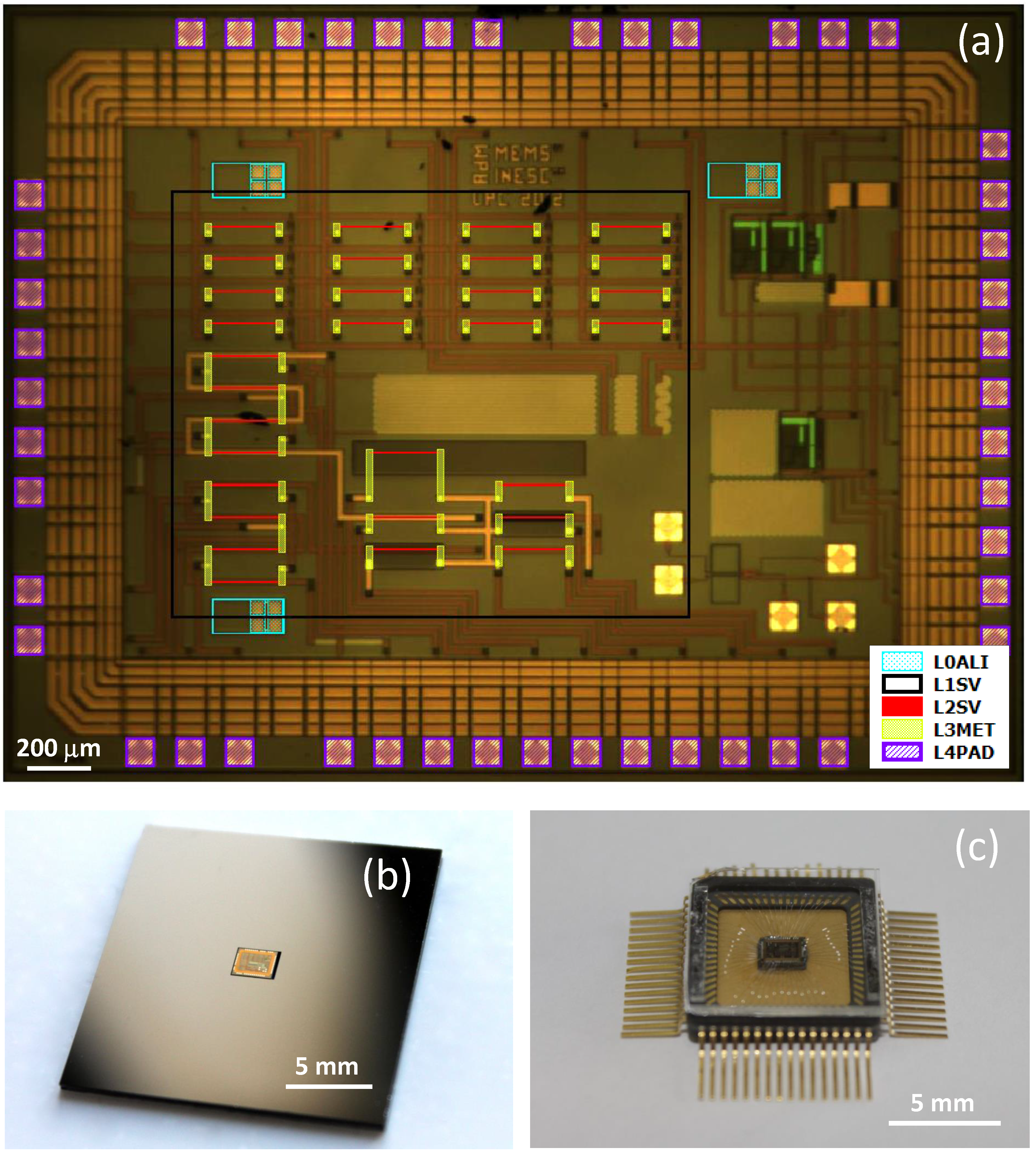
2.2.2. GMR Structures onto Pre-Processed CMOS
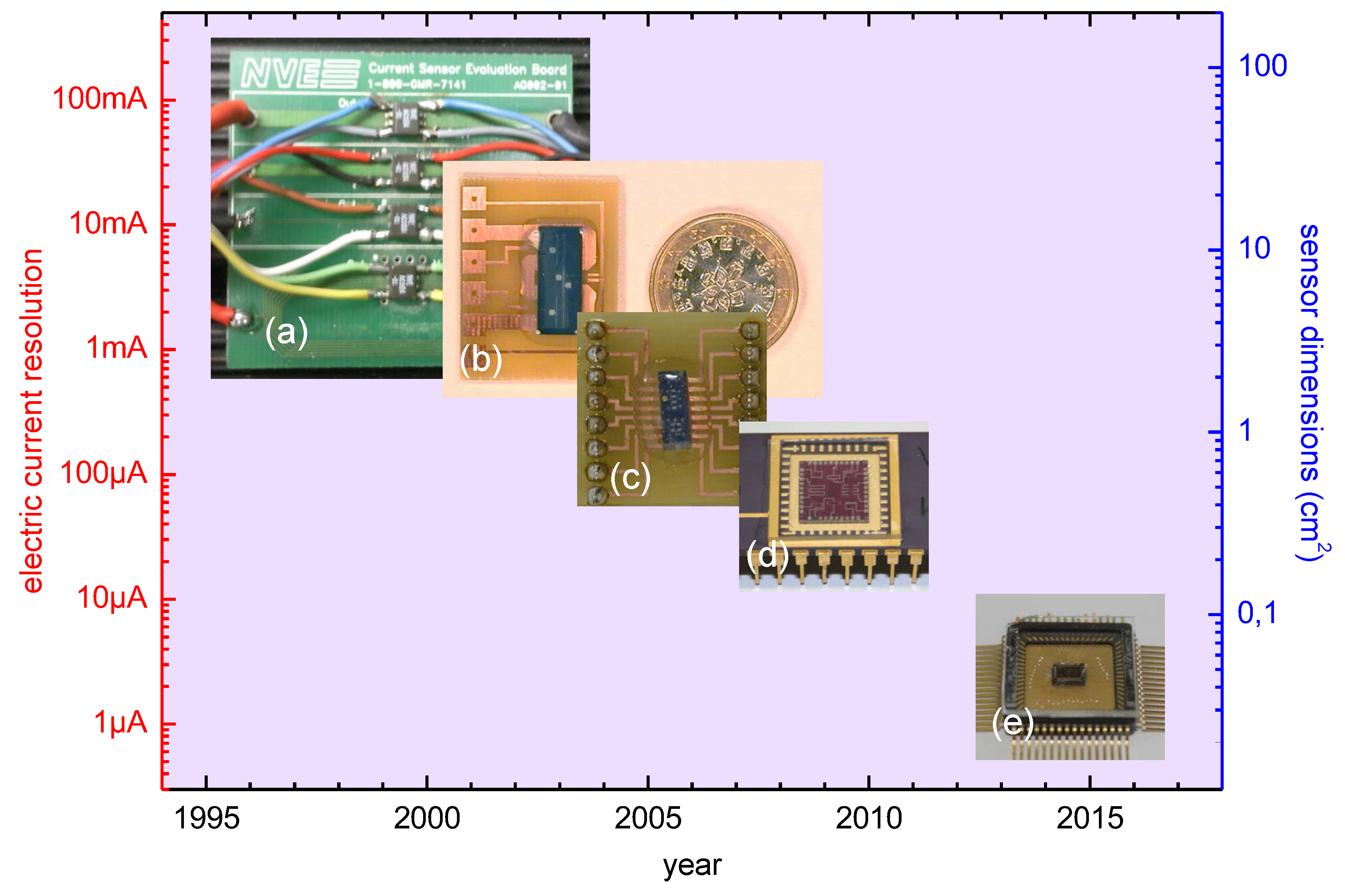
3. Spreading the Performance
3.1. Thermal Drifts
3.2. Limit of Detection
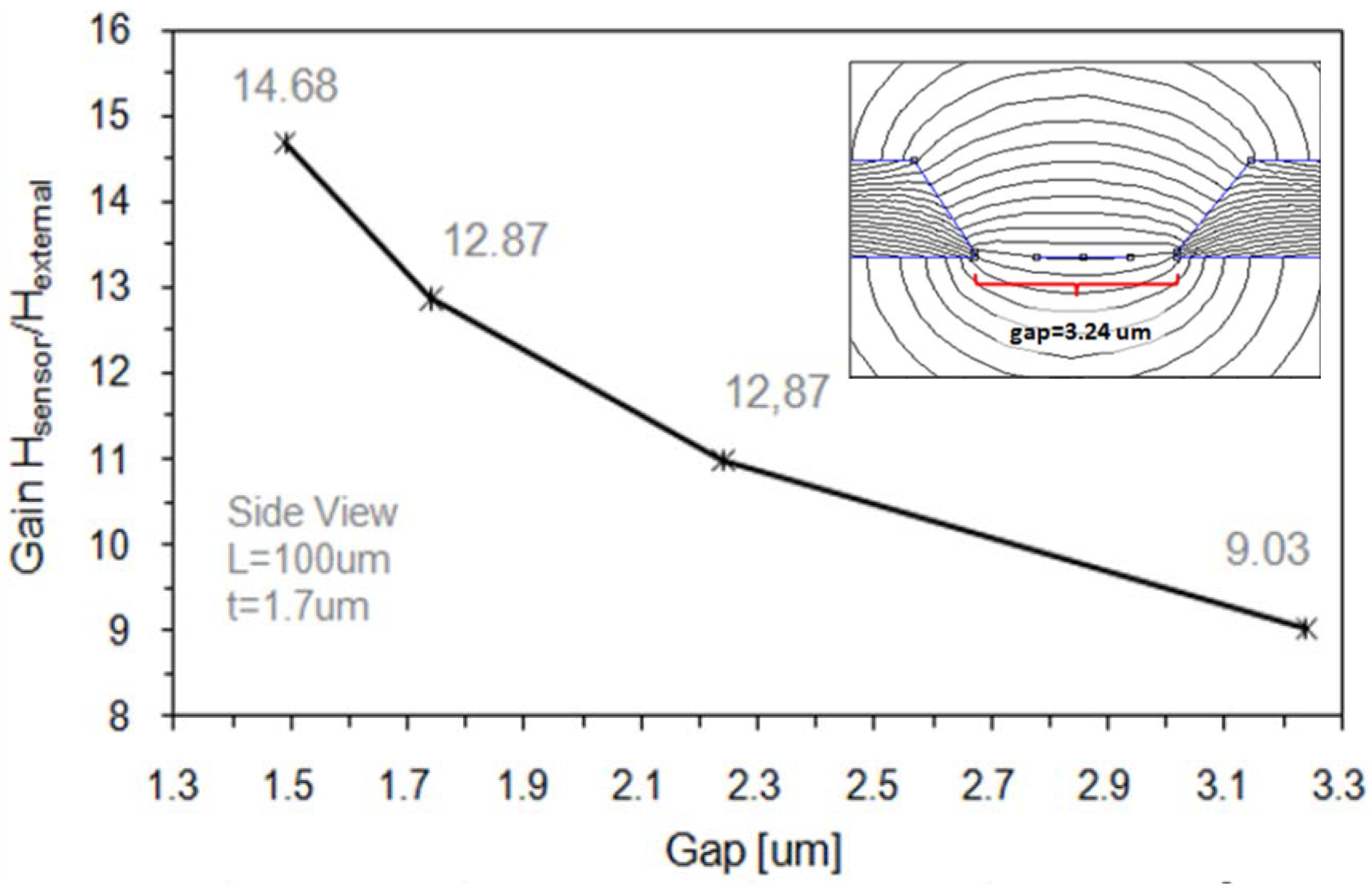
3.2.1. Improving the Sensitivity
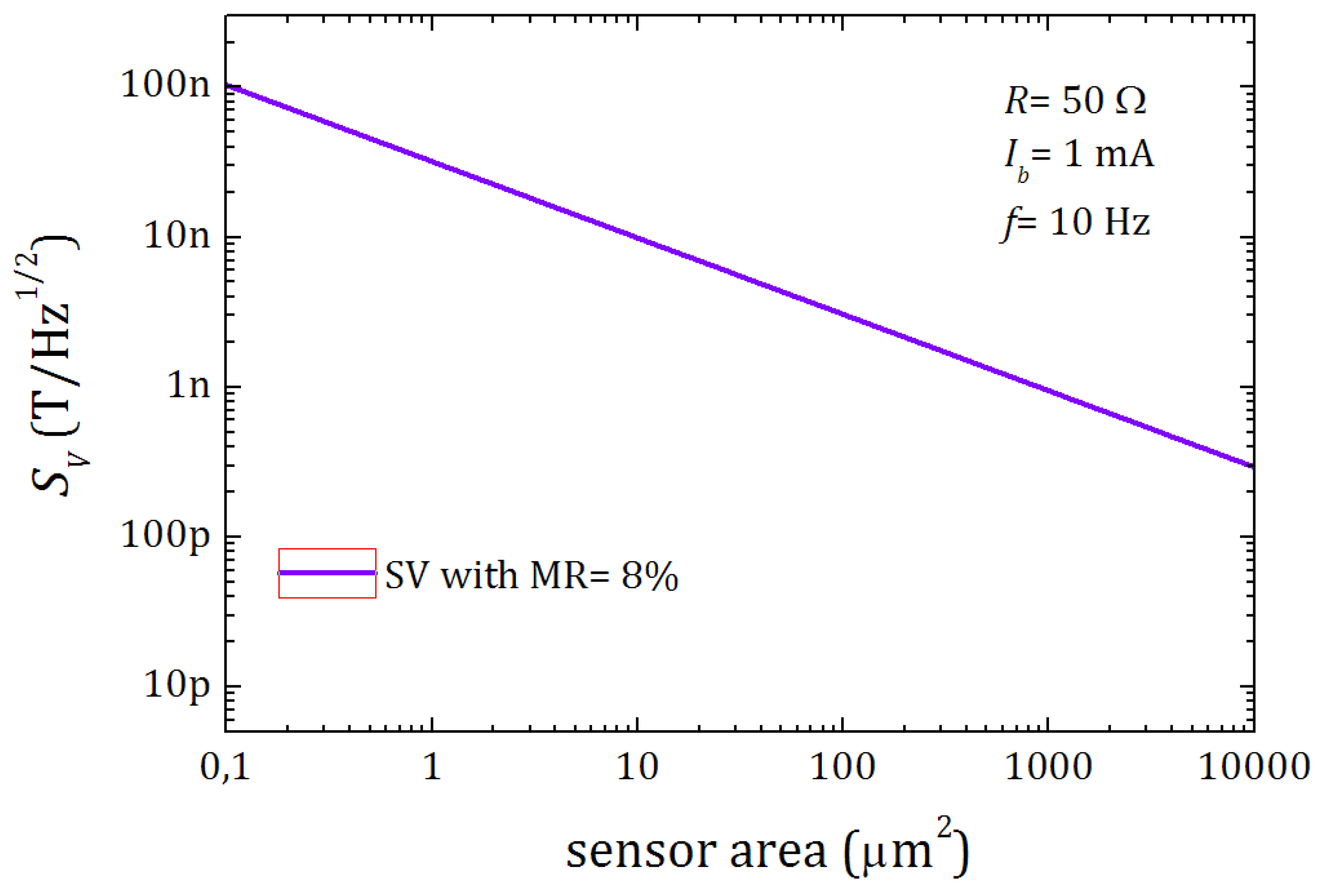
3.2.2. Reducing the Noise
4. Spreading the Range of Application
4.1. Integration with Other Electrical and Electronic Elements
4.1.1. Micro-Strips
4.1.2. Micro-Coils
4.1.3. Antennas
4.1.4. Hall Sensors
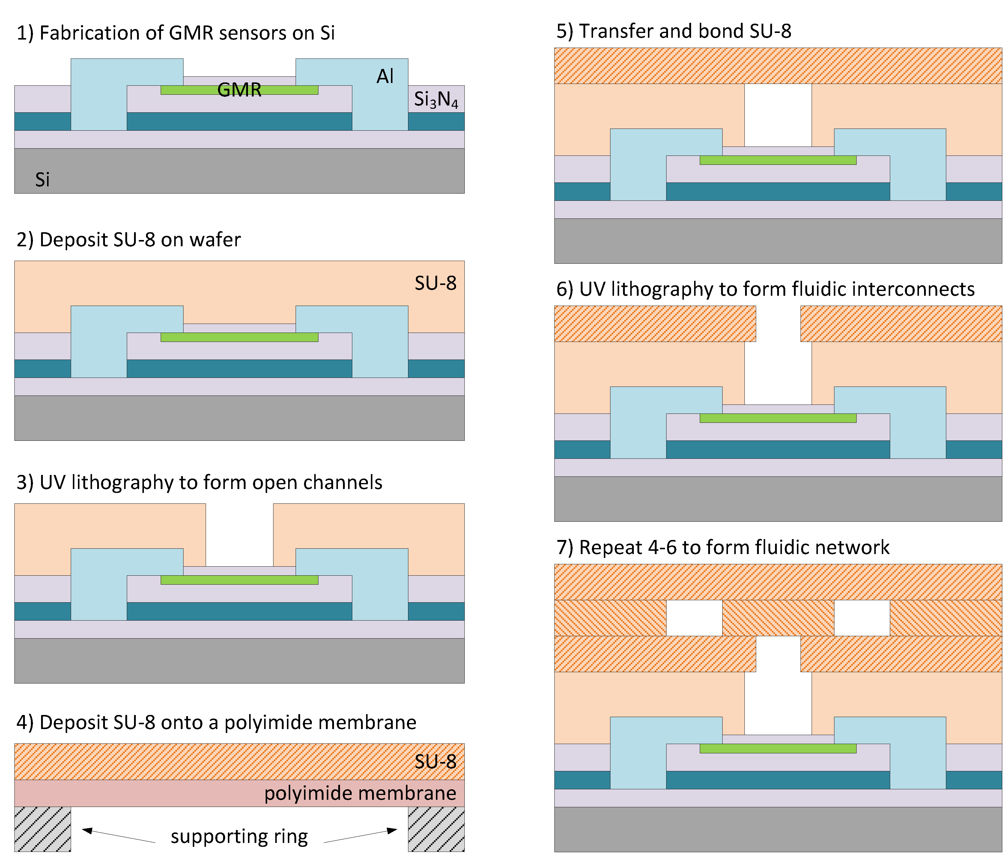
4.2. Microfluidics
4.3. Full Systems
5. Conclusions
Acknowledgments
Author Contributions
Conflicts of Interest
References
- Baibich, M.N.; Broto, J.M.; Fert, A.; Vandau, F.N.; Petroff, F.; Eitenne, P.; Creuzet, G.; Friederich, A.; Chazelas, J. Giant magnetoresistance of (001)Fe/(001)Cr magnetic superlattices. Phys. Rev. Lett. 1988, 61, 2472–2475. [Google Scholar] [CrossRef] [PubMed]
- Binasch, G.; Grunberg, P.; Saurenbach, F.; Zinn, W. Enhanced magnetoresistance in layered magnetic-structures with antiferromagnetic interlayer exchange. Phys. Rev. B 1989, 39, 4828–4830. [Google Scholar] [CrossRef]
- Reig, C.; Cardoso, S.; Mukhopadhyay, S. Giant Magnetoresistance (GMR) Sensors—From Basis to State-of-the-Art Applications; Springer-Verlag: Berlin, Germany; Heidelberg, Germany, 2013. [Google Scholar]
- Freitas, P.P.; Ferreira, R.; Cardoso, S.; Cardoso, F. Magnetoresistive sensors. J. Phys. Condens. Matter 2007, 19, 165221. [Google Scholar] [CrossRef]
- Arana, S.; Arana, N.; Gracia, R.; Castaño, E. High sensitivity linear position sensor developed using granular Ag-Co giant magnetoresistances. Sens. Actuators A Phys. 2005, 123–124, 116–121. [Google Scholar] [CrossRef]
- Peña, V.; Sefrioui, Z.; Arias, D.; Leon, C.; Santamaria, J.; Martinez, J.L.; te Velthuis, S.G.E.; Hoffmann, A. Giant magnetoresistance in ferromagnet/superconductor superlattices. Phys. Rev. Lett. 2005, 94, 057002. [Google Scholar] [CrossRef] [PubMed]
- Pullini, D.; Busquets, D.; Ruotolo, A.; Innocenti, G.; Amigó, V. Insights into pulsed electrodeposition of GMR multilayered nanowires. J. Magn. Magn. Mater. 2007, 316, E242–E245. [Google Scholar] [CrossRef]
- Johnson, J. Thermal agitation of electricity in conductors. Nature 1927, 119, 50–51. [Google Scholar] [CrossRef]
- Nyquist, H. Thermal agitation of electric charge in conductors. Phys. Rev. 1928, 32, 110–113. [Google Scholar] [CrossRef]
- Hooge, F.N. 1/f Noise. Phys. B C 1976, 83, 14–23. [Google Scholar] [CrossRef]
- Cubells-Beltrán, M.D.; Reig, C.; Muñoz, D.R.; Freitas, S.; Freitas, P. Full wheatstone bridge spin-valve based sensors for IC currents monitoring. IEEE Sens. J. 2009, 9, 1756–1762. [Google Scholar] [CrossRef]
- Rajasekaran, N.; Mohan, S. Giant Magnetoresistance in Electrodeposited Films: Current Status and the Influence of Parameters. Crit. Rev. Solid State Mater. Sci. 2012, 37, 158–180. [Google Scholar] [CrossRef]
- Wood, D.; Ni, K.; Schmidt, D.; Cleland, A. Submicron giant magnetoresistive sensors for biological applications. Sens. Actuators A Phys. 2005, 120, 1–6. [Google Scholar] [CrossRef]
- Gangopadhyay, S.; Shen, J.; Kief, M.; Barnard, J.; Parker, M. Giant Magnetoresistance in CoFe/Cu Multilayers with Different Buffer Layers and Substrates. IEEE Trans. Magn. 1995, 31, 3933–3935. [Google Scholar] [CrossRef]
- Parkin, S.S.P.; Roche, K.P.; Suzuki, T. Giant Magnetoresistance in Antiferromagnetic Co/Cu Multilayers Grown on Kapton. Jpn. J. Appl. Phys. 1992, 31, L1246–L1249. [Google Scholar] [CrossRef]
- Parkin, S.S.P. Flexible giant magnetoresistance sensors. Appl. Phys. Lett. 1996, 69, 3092. [Google Scholar] [CrossRef]
- Fonseca, H.; Paz, E.; Ferreira, R.; Cardoso, S.; Gaspar, J.; Freitas, P.P. Flexible magnetoresistive devices with high-performance sensors. In Proceedings of the 41st International Conference Micro & Nano Engineering (MNE 2015), Hague, The Netherlands, 21–24 September 2015.
- Melzer, M.; Makarov, D.; Calvimontes, A.; Karnaushenko, D.; Baunack, S.; Kaltofen, R.; Mei, Y.; Schmidt, O.G. Stretchable magnetoelectronics. Nano Lett. 2011, 11, 2522–2526. [Google Scholar] [CrossRef] [PubMed]
- Melzer, M.; Lin, G.; Makarov, D.; Schmidt, O.G. Stretchable Spin Valves on Elastomer Membranes by Predetermined Periodic Fracture and Random Wrinkling. Adv. Mater. 2012, 24, 6468–6472. [Google Scholar] [CrossRef] [PubMed]
- Donolato, M.; Tollan, C.; Porro, J.M.; Berger, A.; Vavassori, P. Flexible and stretchable polymers with embedded magnetic nanostructures. Adv. Mater. 2013, 25, 623–629. [Google Scholar] [CrossRef] [PubMed]
- Karnaushenko, D.; Makarov, D.; Yan, C.; Streubel, R.; Schmidt, O.G. Printable giant magnetoresistive devices. Adv. Mater. 2012, 24, 4518–4522. [Google Scholar] [CrossRef] [PubMed]
- Karnaushenko, D.; Makarov, D.; Stöber, M.; Karnaushenko, D.D.; Baunack, S.; Schmidt, O.G. High-performance magnetic sensorics for printable and flexible electronics. Adv. Mater. 2015, 27, 880–885. [Google Scholar] [CrossRef] [PubMed]
- Makarov, D.; Melzer, M.; Karnaushenko, D.; Schmidt, O.G. Shapeable magnetoelectronics. Appl. Phys. Rev. 2016, 3, 011101. [Google Scholar] [CrossRef]
- Brown, J. A universal low-field magnetic field sensor using GMR resistors on a semicustom BiCMOS array. In Proceedings of the 39th Midwest Symposium on Circuits and Systems, Ames, IA, USA, 18–21 August 1996; pp. 123–126.
- Han, S.J.; Xu, L.; Yu, H.; Wilson, R.J.; White, R.L.; Pourmand, N.; Wang, S.X. CMOS integrated DNA Microarray based on GMR sensors. In Proceedings of the 2006 International Electron Devices Meeting, San Francisco, CA, USA, 11–13 December 2006; pp. 451–454.
- Cubells-Beltrán, M.D.; Reig, C.; De Marcellis, A.; Figueras, E.; Yúfera, A.; Zadov, B.; Paperno, E.; Cardoso, S.; Freitas, P.P. Monolithic integration of Giant Magnetoresistance (GMR) devices onto standard processed CMOS dies. Microelectron. J. 2014, 45, 702–707. [Google Scholar] [CrossRef]
- Cardoso, F.A.; Costa, T.; Germano, J.; Cardoso, S.; Borme, J.; Gaspar, J.; Fernandes, J.R.; Piedade, M.S.; Freitas, P.P. Integration of Magnetoresistive Biochips on a CMOS Circuit. IEEE Trans. Magn. 2012, 48, 3784–3787. [Google Scholar] [CrossRef]
- Hall, D.A.; Gaster, R.S.; Makinwa, K.; Wang, S.X.; Murmann, B. A 256 pixel magnetoresistive biosensor microarray in 0.18 μm CMOS. IEEE J. Solid-State Circuits 2013, 48, 1290–1301. [Google Scholar] [CrossRef] [PubMed]
- Marcellis, A.D.; Reig, C.; Cubells, M.D.; Madrenas, J.; Cardoso, F.; Cardoso, S.; Freitas, P.P. Giant Magnetoresistance (GMR) sensors for 0.35 μm CMOS technology sub-mA current sensing. In Proceedings of the 2014 IEEE Sensors, Valencia, Spain, 2–5 November 2014; pp. 444–447.
- De Marcellis, A.; Cubells-Beltrán, M.D.; Reig, C.; Madrenas, J.; Zadov, B.; Paperno, E.; Cardoso, S.; Freitas, P.P. Quasi-digital front-ends for current measurement in integrated circuits with giant magnetoresistance technology. IET Circuits Devices Syst. 2014, 8, 291–300. [Google Scholar] [CrossRef]
- Chen, T.; Eklund, A.; Sani, S.; Rodriguez, S.; Malm, B.G.; Åkerman, J.; Rusu, A. Integration of GMR-based spin torque oscillators and CMOS circuitry. Solid-State Electron. 2015, 111, 91–99. [Google Scholar] [CrossRef]
- Cubells-Beltrán, M.D.; Reig, C.; Martos, J.; Torres, J.; Soret, J. Limitations of Magnetoresistive Current Sensors in Industrial Electronics Applications. Int. Rev. Electr. Eng. 2011, 6, 423–429. [Google Scholar]
- Roldán, A.M.; Roldán, J.B.; Reig, C.; Cubells-Beltrán, M.D.; Ramírez, D.; Cardoso, S.; Freitas, P.P. A DC behavioral electrical model for quasi-linear spin-valve devices including thermal effects for circuit simulation. Microelectron. J. 2011, 42, 365–370. [Google Scholar]
- Reig, C.; Ramírez, D.; Silva, F.; Bernardo, J.; Freitas, P.P. Design, fabrication, and analysis of a spin-valve based current sensor. Sens. Actuators A Phys. 2004, 115, 259–266. [Google Scholar]
- Sánchez Moreno, J.; Ramírez Muñoz, D.; Cardoso, S.; Casans Berga, S.; Navarro Antón, A.E.; Peixeiro de Freitas, P.J. A non-invasive thermal drift compensation technique applied to a spin-valve magnetoresistive current sensor. Sensors 2011, 11, 2447–2458. [Google Scholar]
- Freitas, P.P.; Cardoso, S.; Ferreira, R.; Martins, V.C.; Guedes, A.; Cardoso, F.A.; Loureiro, J.; Macedo, R.; Chaves, R.C.; Amaral, J. Optimization and integration of magnetoresistive sensors. SPIN 2011, 1, 71–91. [Google Scholar] [CrossRef]
- Chen, J.; Wurz, M.C.; Belski, A.; Rissing, L. Designs and Characterizations of Soft Magnetic Flux Guides in a 3-D Magnetic Field Sensor. IEEE Trans. Magn. 2012, 48, 1481–1484. [Google Scholar] [CrossRef]
- Jeng, J.T.; Chiang, C.Y.; Chang, C.H.; Lu, C.C. Vector Magnetometer with Dual-Bridge GMR Sensors. IEEE Trans. Magn. 2014, 50, 1–4. [Google Scholar] [CrossRef]
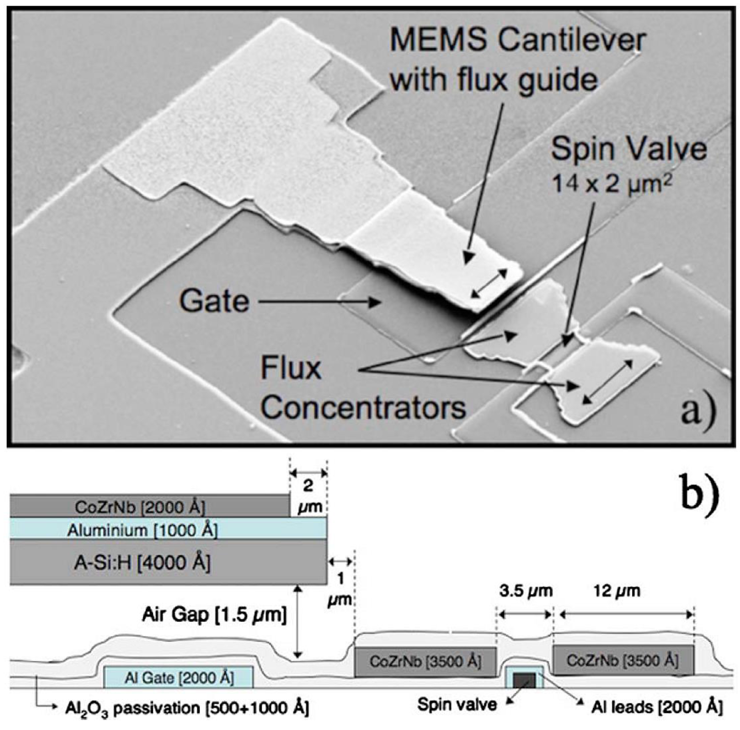
- Edelstein, A.S.; Fischer, G.A. Minimizing 1/f noise in magnetic sensors using a microelectromechanical system flux concentrator. J. Appl. Phys. 2002, 91, 7795. [Google Scholar] [CrossRef]
- Guedes, A.; Patil, S.B.; Cardoso, S.; Chu, V.; Conde, J.P.; Freitas, P.P. Hybrid magnetoresistive microelectromechanical devices for static field modulation and sensor 1/f noise cancellation. J. Appl. Phys. 2008, 103, 07E924. [Google Scholar] [CrossRef]
- Guedes, A.; Jaramillo, G.; Buffa, C.; Vigevani, G.; Cardoso, S.; Leitao, D.C.; Freitas, P.P.; Horsley, D.A. Towards picoTesla Magnetic Field Detection Using a GMR-MEMS Hybrid Device. IEEE Trans. Magn. 2012, 48, 4115–4118. [Google Scholar] [CrossRef]
- Reig, C.; Cubells-Beltran, M.D.; Muñoz, D.R. Magnetic Field Sensors Based on Giant Magnetoresistance (GMR) Technology: Applications in Electrical Current Sensing. Sensors 2009, 9, 7919–7942. [Google Scholar] [CrossRef] [PubMed]
- Reig, C.; Ramirez, D.; Li, H.; Freitas, P. Low-current sensing with specular spin valve structures. IET Circuits Devices Syst. 2005, 152, 307. [Google Scholar] [CrossRef]
- Rifai, D.; Abdalla, A.N.; Ali, K.; Razali, R. Giant Magnetoresistance Sensors: A Review on Structures and Non-Destructive Eddy Current Testing Applications. Sensors 2016, 16, 298. [Google Scholar] [CrossRef] [PubMed]
- Freitas, P.P.; Cardoso, F.A.; Martins, V.C.; Martins, S.A.M.; Loureiro, J.; Amaral, J.; Chaves, R.C.; Cardoso, S.; Fonseca, L.P.; Sebastião, A.M.; et al. Spintronic platforms for biomedical applications. Lab Chip 2012, 12, 546–557. [Google Scholar] [CrossRef] [PubMed]
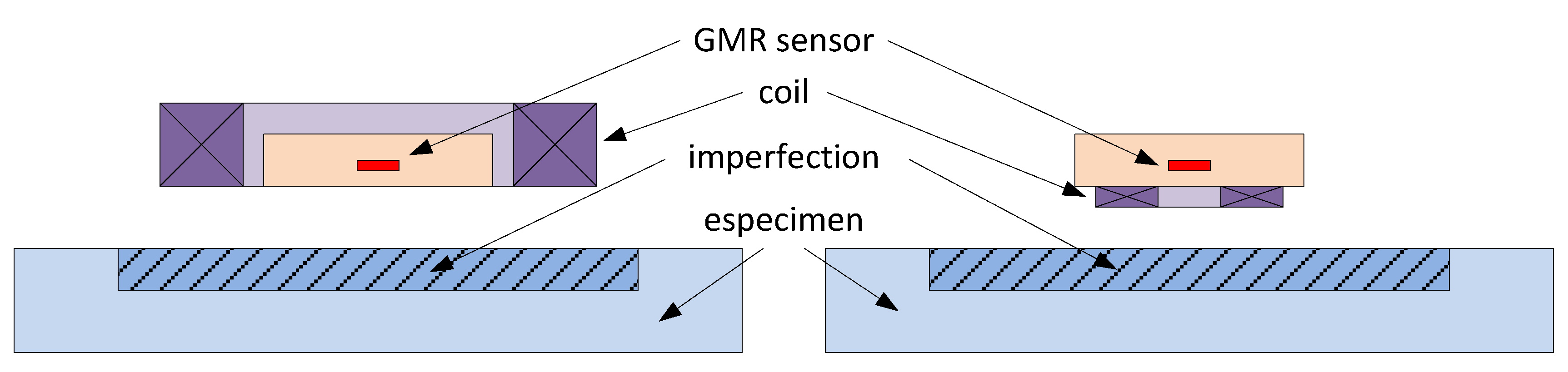
- Cacciola, M.; Megali, G.; Pellicanó, D.; Morabito, F.C. A GMR-ECT based embedded solution for applications on PCB inspections. Sens. Actuators A Phys. 2011, 167, 25–33. [Google Scholar] [CrossRef]
- Pasadas, D.; Rocha, T.J.; Ramos, H.G.; Ribeiro, A.L. Evaluation of portable ECT instruments with positioning capability. Measurement 2012, 45, 393–404. [Google Scholar] [CrossRef]
- Zeng, Z.; Deng, Y.; Liu, X.; Udpa, L.; Udpa, S.S.; Koltenbah, B.E.C.; Bossi, R.H.; Steffes, G. EC-GMR Data Analysis for Inspection of Multilayer Airframe Structures. IEEE Trans. Magn. 2011, 47, 4745–4752. [Google Scholar] [CrossRef]
- Gooneratne, C.P.; Liang, C.; Kosel, J. A planar conducting microstructure to guide and confine magnetic beads to a sensing zone. Microelectron. Eng. 2011, 88, 1757–1760. [Google Scholar] [CrossRef]
- Gooneratne, C.P.; Liang, C.; Giouroudi, I.; Kosel, J. An integrated micro-chip for rapid detection of magnetic particles. J. Appl. Phys. 2012, 111, 07B327. [Google Scholar] [CrossRef]
- Macedo, R.; Cardoso, S.; Freitas, P.P.; Germano, J.; Piedade, M.S. Hybrid antenna-magnetoresistive sensor for radio frequency field detection. J. Appl. Phys. 2011, 109, 07E505. [Google Scholar] [CrossRef]
- Macedo, R.; Cardoso, F.A.; Cardoso, S.; Freitas, P.P.; Germano, J.; Piedade, M.S. Self-powered, hybrid antenna-magnetoresistive sensor for magnetic field detection. Appl. Phys. Lett. 2011, 98, 103503. [Google Scholar] [CrossRef]
- Kim, J.; Lee, J.; Jun, J.; Le, M.; Cho, C. Integration of Hall and Giant Magnetoresistive Sensor Arrays for Real-Time 2-D Visualization of Magnetic Field Vectors. IEEE Trans. Magn. 2012, 48, 3708–3711. [Google Scholar] [CrossRef]
- Angani, C.S.; Kim, J.; Le, M.; Lee, J. Magnetic Leakage Testing Using Linearly Integrated Hall and GMR Sensor Arrays to Inspect Inclusions in Cold-Rolled Strips. IEEE Trans. Magn. 2014, 50, 1–4. [Google Scholar] [CrossRef]
- Giouroudi, I.; Keplinger, F. Microfluidic biosensing systems using magnetic nanoparticles. Int. J. Mol. Sci. 2013, 14, 18535–18556. [Google Scholar] [CrossRef] [PubMed]
- Peng, Z.; Ling, Z.; Tondra, M.; Liu, C.; Zhang, M.; Lian, K.; Goettert, J.; Hormes, J. CMOS Compatible Integration of Three-Dimensional Microfluidic Systems Based on Low-Temperature Transfer of SU-8 Films. J. Microelectromech. Syst. 2006, 15, 708–716. [Google Scholar] [CrossRef]
- Schotter, J.; Shoshi, A.; Brueckl, H. Development of a magnetic lab-on-a-chip for point-of-care sepsis diagnosis. J. Magn. Magn. Mater. 2009, 321, 1671–1675. [Google Scholar] [CrossRef]
- Hall, D.A.; Gaster, R.S.; Osterfeld, S.J.; Murmann, B.; Wang, S.X. GMR biosensor arrays: Correction techniques for reproducibility and enhanced sensitivity. Biosens. Bioelectron. 2010, 25, 2177–2181. [Google Scholar] [CrossRef] [PubMed]
- Kokkinis, G.; Cardoso, S.F.; Cardoso, F.A.; Giouroudi, I. Microfluidics for the Rapid Detection of Pathogens Using Giant Magnetoresistance Sensors. IEEE Trans. Magn. 2014, 50, 1–4. [Google Scholar] [CrossRef]
- Wimberger-Friedl, R.; Nellissen, T.; Weekamp, W.; van Delft, J.; Ansems, W.; Prins, M.; Megens, M.; Dittmer, W.; de Witz, C.; van Iersel, B. Packaging of silicon sensors for microfluidic bio-analytical applications. J. Micromech. Microeng. 2009, 19, 015015. [Google Scholar] [CrossRef]
- Chaves, R.C.; Bensimon, D.; Freitas, P.P. Single molecule actuation and detection on a lab-on-a-chip magnetoresistive platform. J. Appl. Phys. 2011, 109, 064702. [Google Scholar] [CrossRef]
- Muluneh, M.; Issadore, D. A multi-scale PDMS fabrication strategy to bridge the size mismatch between integrated circuits and microfluidics. Lab Chip 2014, 14, 4552–4558. [Google Scholar] [CrossRef] [PubMed]
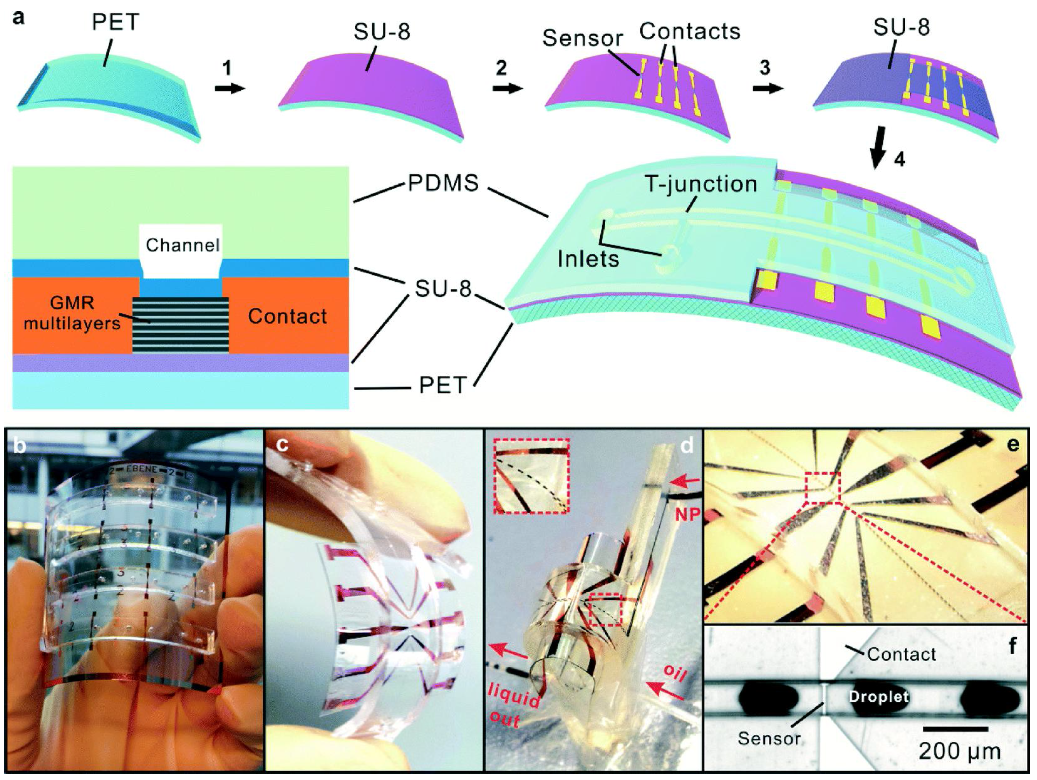
- Lin, G.; Makarov, D.; Melzer, M.; Si, W.; Yan, C.; Schmidt, O.G. A highly flexible and compact magnetoresistive analytic device. Lab Chip 2014, 14, 4050–4058. [Google Scholar] [CrossRef] [PubMed]
- Martins, V.C.; Germano, J.; Cardoso, F.A.; Loureiro, J.; Cardoso, S.; Sousa, L.; Piedade, M.; Fonseca, L.P.; Freitas, P. Challenges and trends in the development of a magnetoresistive biochip portable platform. J. Magn. Magn. Mater. 2010, 322, 1655–1663. [Google Scholar] [CrossRef]
- Costa, T.; Piedade, M.S.; Germano, J.; Amaral, J.; Freitas, P.P. A Neuronal Signal Detector for Biologically Generated Magnetic Fields. IEEE Trans. Instrum. Meas. 2014, 63, 1171–1180. [Google Scholar] [CrossRef]
- Betta, G.; Ferrigno, L.; Laracca, M. GMR-Based ECT Instrument for Detection and Characterization of Crack on a Planar Specimen: A Hand-Held Solution. IEEE Trans. Instrum. Meas. 2012, 61, 505–512. [Google Scholar] [CrossRef]
- Huo, W.; Gao, Y.; Zhang, L.; Shi, S.; Gao, Y. A Novel High-Sensitivity Cardiac Multibiomarker Detection System Based on Microfluidic Chip and GMR Sensors. IEEE Trans. Magn. 2015, 51, 1–4. [Google Scholar] [CrossRef]
- Wang, W.; Wang, Y.; Tu, L.; Feng, Y.; Klein, T.; Wang, J.P. Magnetoresistive performance and comparison of supermagnetic nanoparticles on giant magnetoresistive sensor-based detection system. Sci. Rep. 2014, 4, 5716. [Google Scholar] [CrossRef] [PubMed]
- Lin, G.; Makarov, D.; Medina-Sánchez, M.; Guix, M.; Baraban, L.; Cuniberti, G.; Schmidt, O.G. Magnetofluidic platform for multidimensional magnetic and optical barcoding of droplets. Lab Chip 2015, 15, 216–224. [Google Scholar] [CrossRef] [PubMed]
- Wang, Y.; Wang, W.; Yu, L.; Tu, L.; Feng, Y.; Klein, T.; Wang, J.P. Giant magnetoresistive-based biosensing probe station system for multiplex protein assays. Biosens. Bioelectron. 2015, 70, 61–68. [Google Scholar] [CrossRef] [PubMed]


© 2016 by the authors; licensee MDPI, Basel, Switzerland. This article is an open access article distributed under the terms and conditions of the Creative Commons Attribution (CC-BY) license (http://creativecommons.org/licenses/by/4.0/).
Share and Cite
Cubells-Beltrán, M.-D.; Reig, C.; Madrenas, J.; De Marcellis, A.; Santos, J.; Cardoso, S.; Freitas, P.P. Integration of GMR Sensors with Different Technologies. Sensors 2016, 16, 939. https://doi.org/10.3390/s16060939
Cubells-Beltrán M-D, Reig C, Madrenas J, De Marcellis A, Santos J, Cardoso S, Freitas PP. Integration of GMR Sensors with Different Technologies. Sensors. 2016; 16(6):939. https://doi.org/10.3390/s16060939
Chicago/Turabian StyleCubells-Beltrán, María-Dolores, Càndid Reig, Jordi Madrenas, Andrea De Marcellis, Joana Santos, Susana Cardoso, and Paulo P. Freitas. 2016. "Integration of GMR Sensors with Different Technologies" Sensors 16, no. 6: 939. https://doi.org/10.3390/s16060939
APA StyleCubells-Beltrán, M.-D., Reig, C., Madrenas, J., De Marcellis, A., Santos, J., Cardoso, S., & Freitas, P. P. (2016). Integration of GMR Sensors with Different Technologies. Sensors, 16(6), 939. https://doi.org/10.3390/s16060939