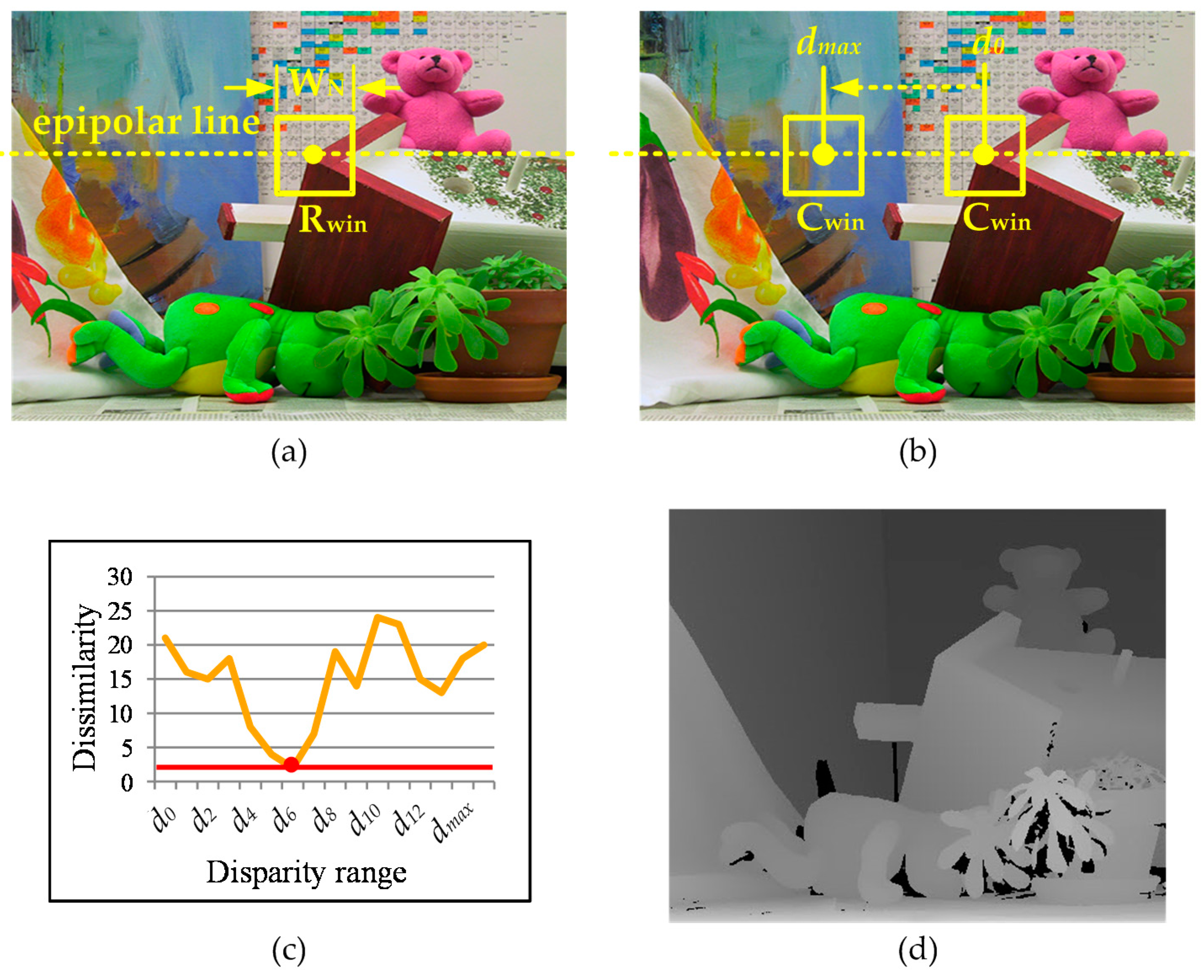
Figure 1.
(a) Left image (Rwin: reference window); (b) right image (dx: disparity range, Cwin: candidate window); (c) dissimilarity between Rwin and Cwin; and (d) a depth map.
Figure 1.
(a) Left image (Rwin: reference window); (b) right image (dx: disparity range, Cwin: candidate window); (c) dissimilarity between Rwin and Cwin; and (d) a depth map.
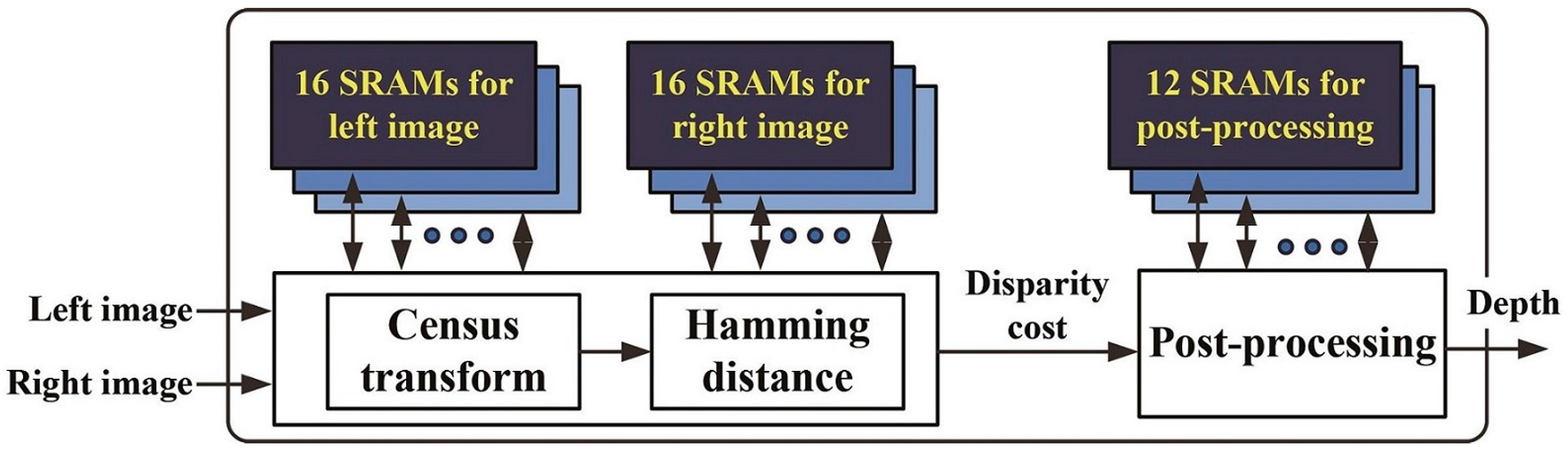
Figure 2.
Flow diagram of the stereo matching processor.
Figure 2.
Flow diagram of the stereo matching processor.
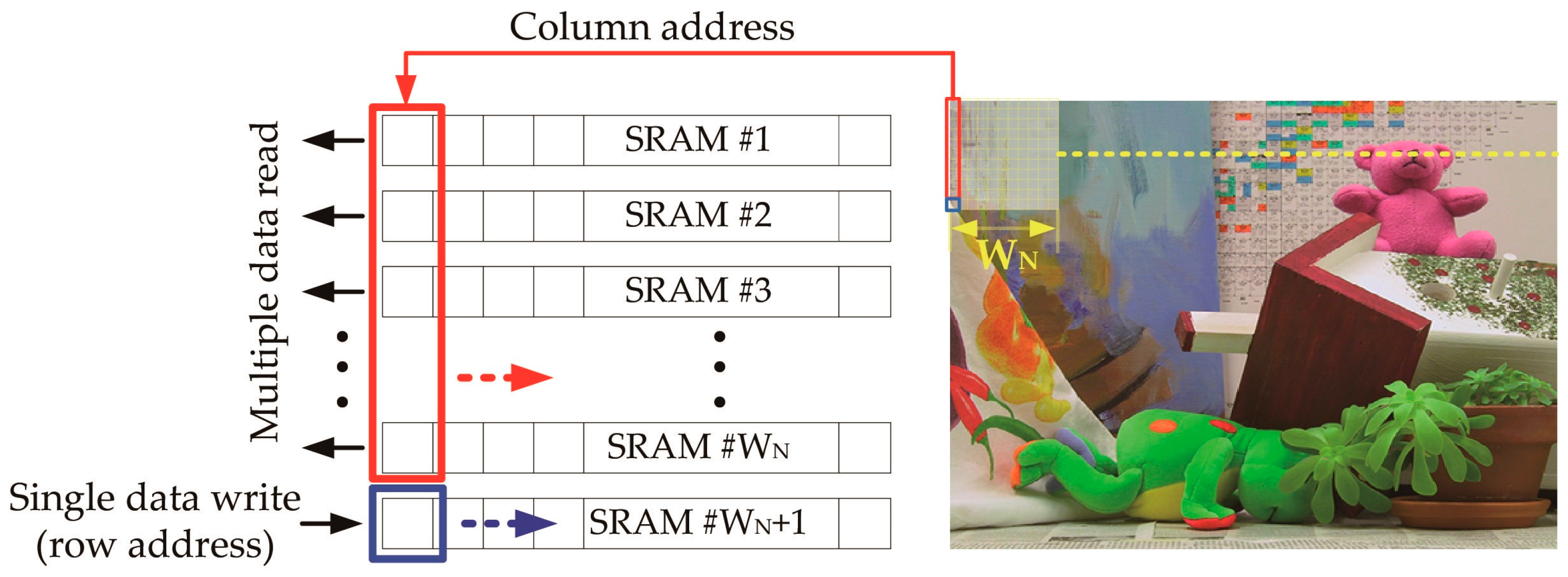
Figure 3.
Illustration of the multiple-read, single-write operation of the stereo matching algorithm.
Figure 3.
Illustration of the multiple-read, single-write operation of the stereo matching algorithm.
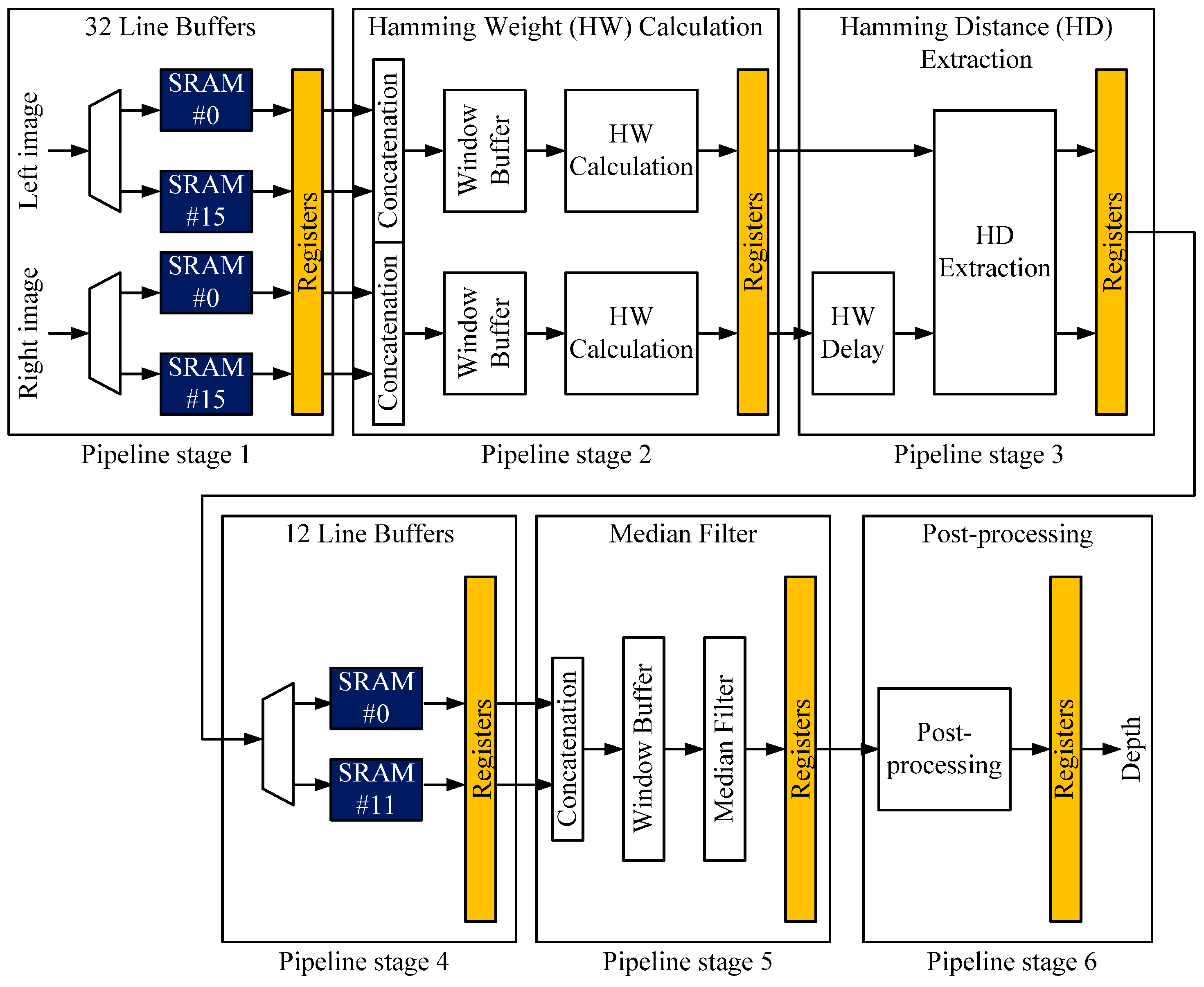
Figure 4.
Pipelined hardware architecture of our stereo matching processor.
Figure 4.
Pipelined hardware architecture of our stereo matching processor.
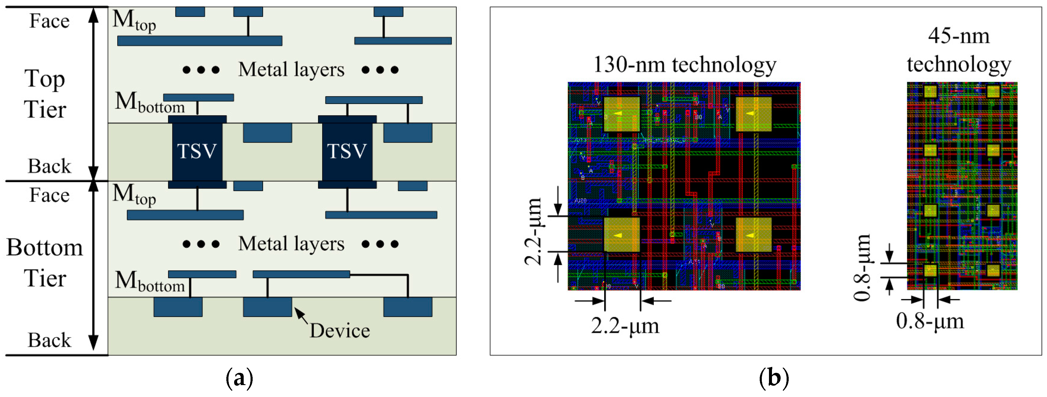
Figure 5.
Via-first bonding technology used in this paper: (a) Side view of via-first TSVs; and (b) top-down view of TSVs.
Figure 5.
Via-first bonding technology used in this paper: (a) Side view of via-first TSVs; and (b) top-down view of TSVs.
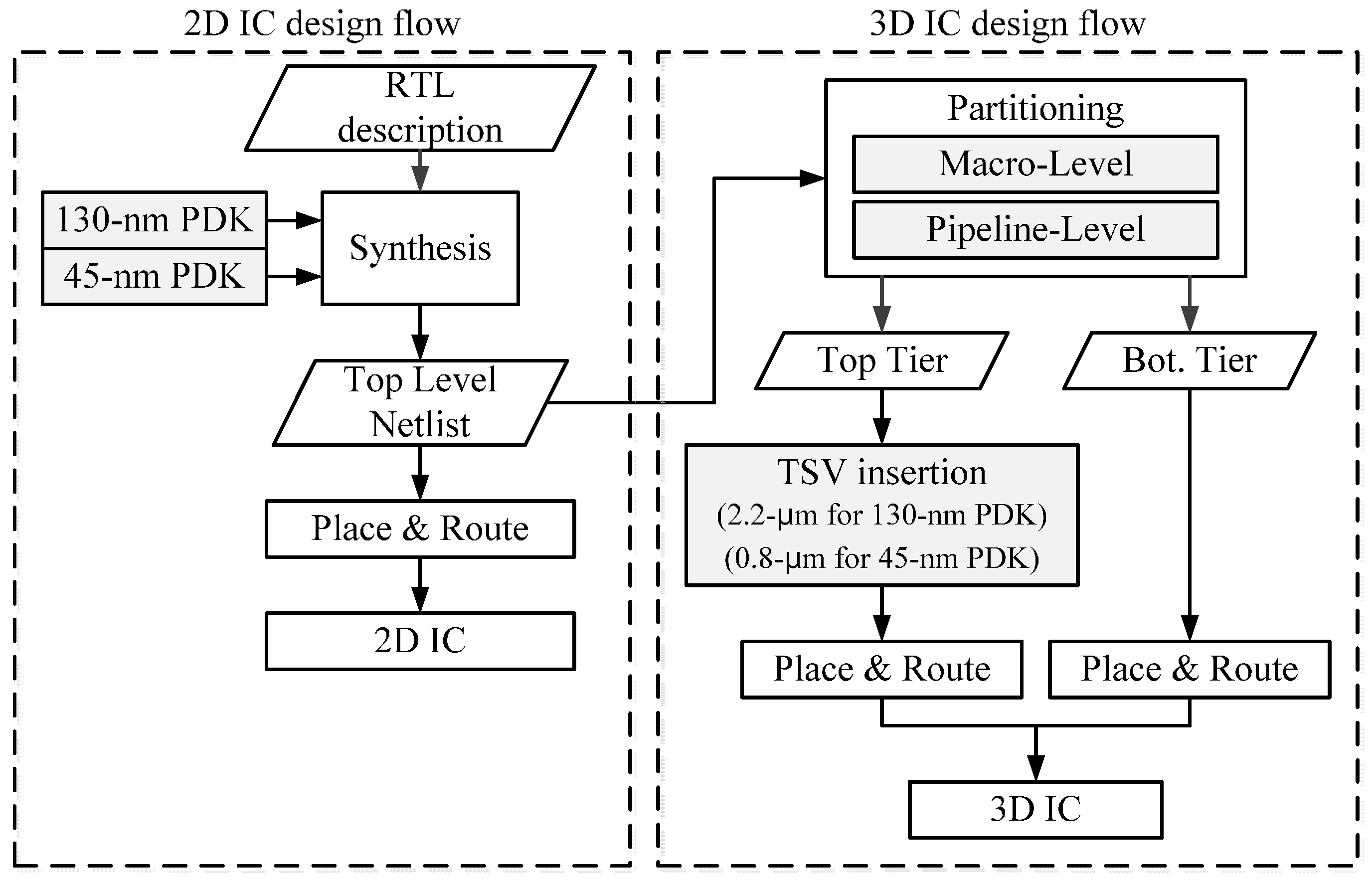
Figure 6.
2D and 3D IC design flow.
Figure 6.
2D and 3D IC design flow.
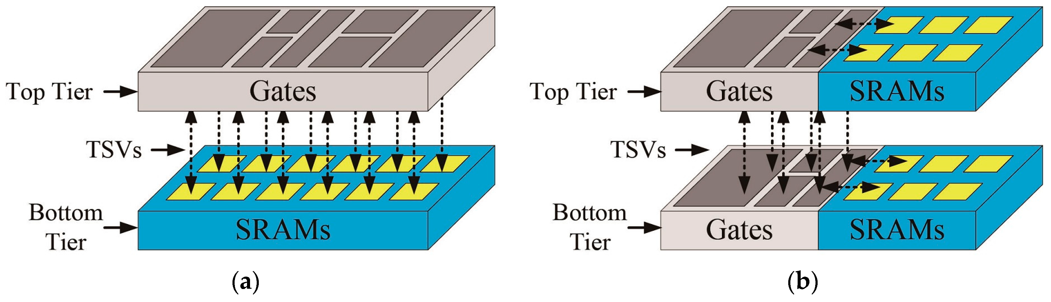
Figure 7.
(a) The conventional macro-level partitioning method; and (b) the proposed pipeline-level partitioning method.
Figure 7.
(a) The conventional macro-level partitioning method; and (b) the proposed pipeline-level partitioning method.
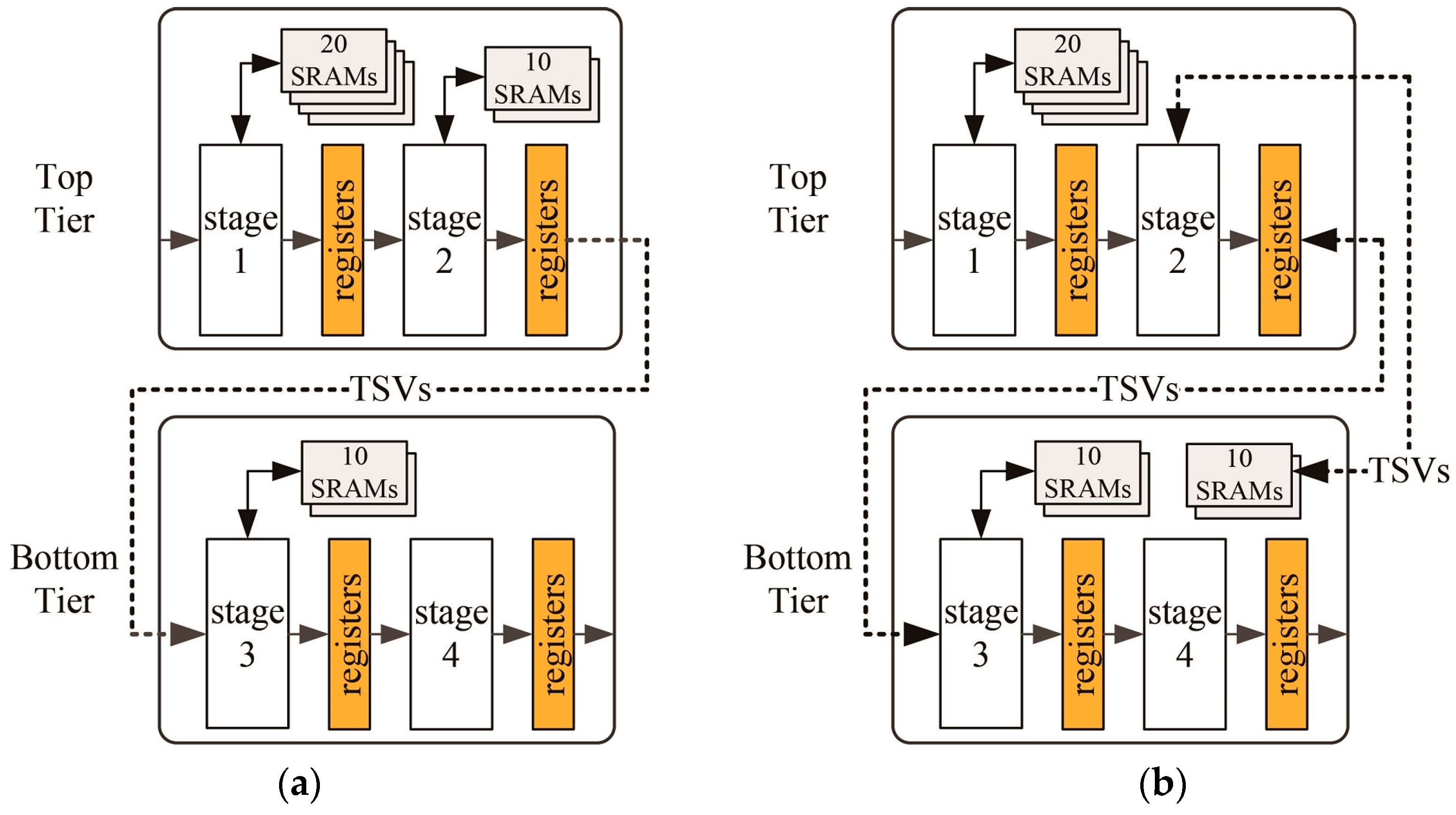
Figure 8.
An illustration of the proposed pipeline-level partitioning method: (a) Split the pipeline stages into two tiers, and (b) adjust the number of SRAMs in each tier.
Figure 8.
An illustration of the proposed pipeline-level partitioning method: (a) Split the pipeline stages into two tiers, and (b) adjust the number of SRAMs in each tier.
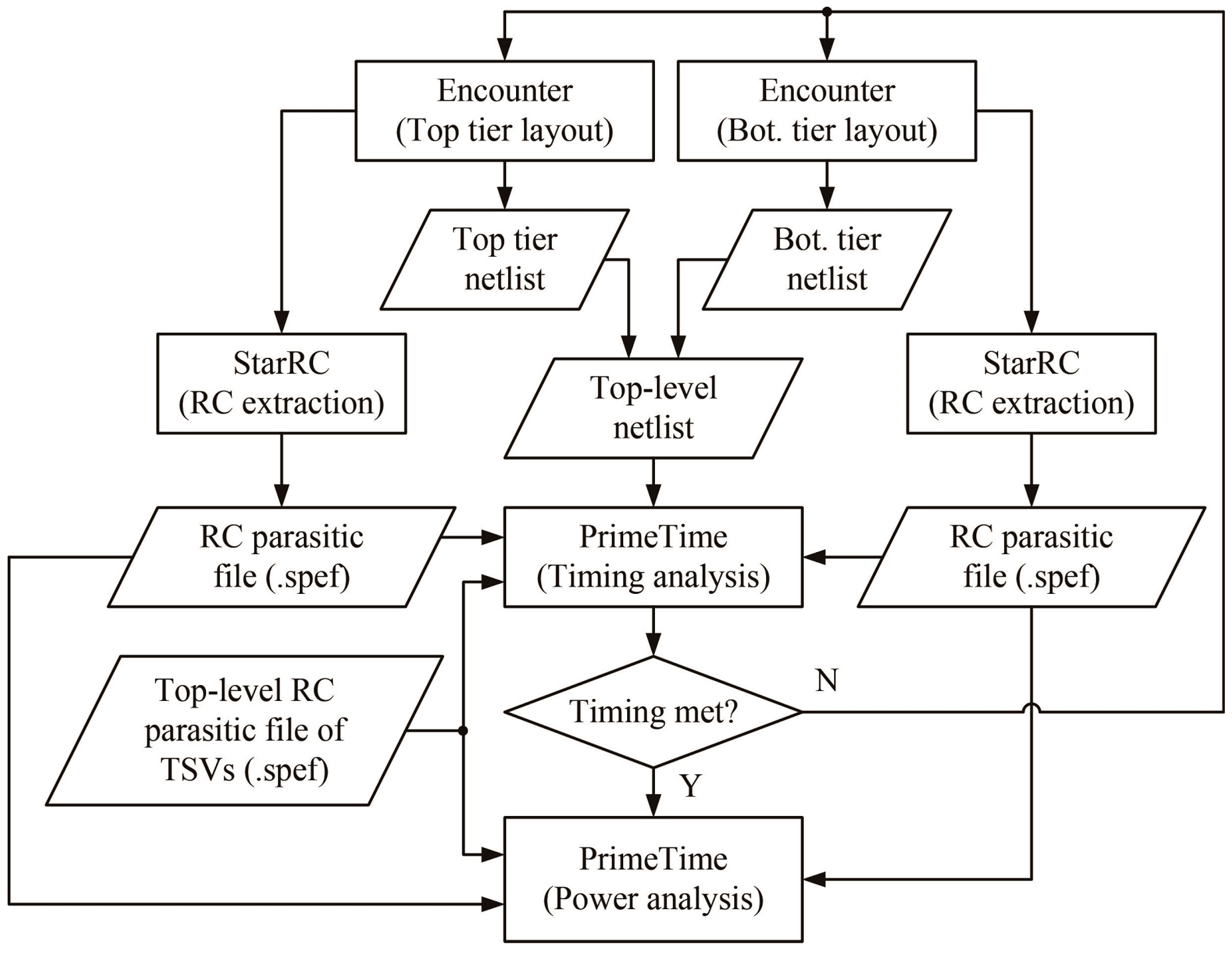
Figure 9.
Overall flow of the power and timing analyses for a 3D IC.
Figure 9.
Overall flow of the power and timing analyses for a 3D IC.
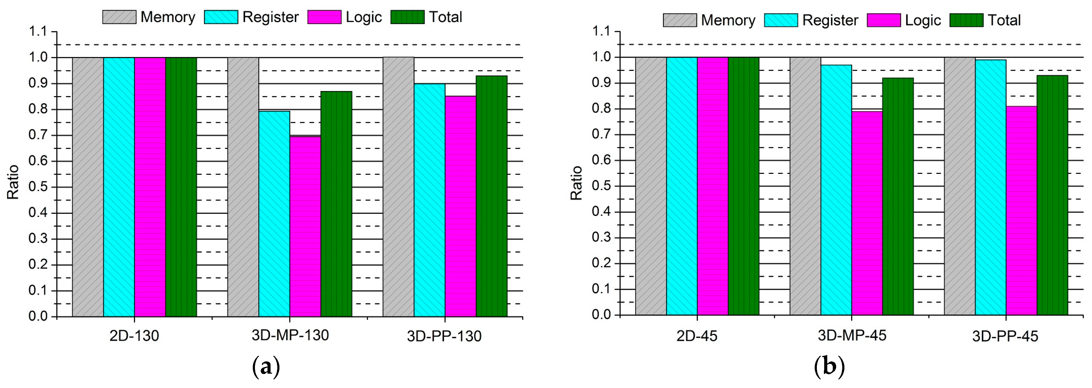
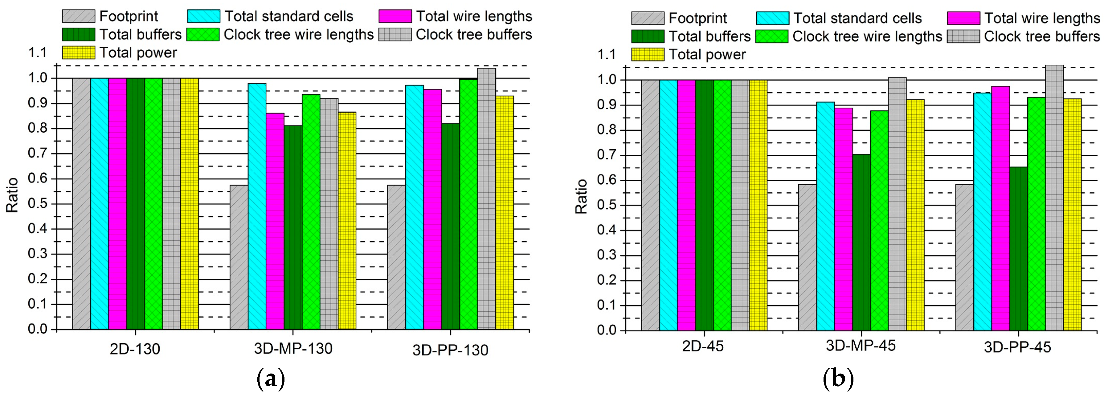
Figure 10.
Comparisons between the normalized designs of 2D and 3D ICs: (a) 2D and 3D ICs designed in 130-nm process technology; and (b) 2D and 3D ICs designed in 45-nm process technology.
Figure 10.
Comparisons between the normalized designs of 2D and 3D ICs: (a) 2D and 3D ICs designed in 130-nm process technology; and (b) 2D and 3D ICs designed in 45-nm process technology.
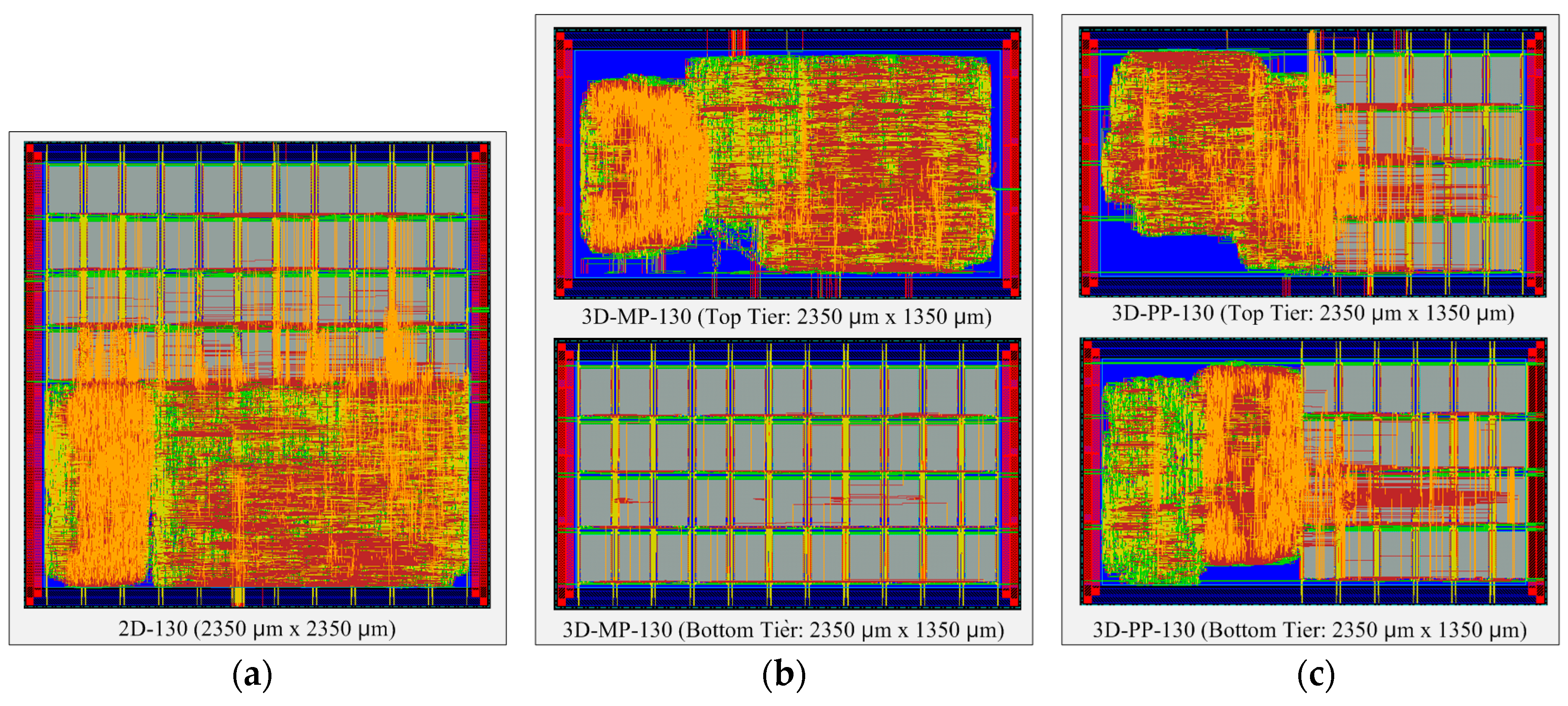
Figure 11.
Layout snapshots of 2D and 3D ICs designed in 130-nm process technology: (a) 2D IC (2D-130); (b) the top and bottom tiers of a 3D IC using macro-level partitioning (3D-MP-130); and (c) the top and bottom tiers of a 3D IC using pipeline-level partitioning (3D-PP-130).
Figure 11.
Layout snapshots of 2D and 3D ICs designed in 130-nm process technology: (a) 2D IC (2D-130); (b) the top and bottom tiers of a 3D IC using macro-level partitioning (3D-MP-130); and (c) the top and bottom tiers of a 3D IC using pipeline-level partitioning (3D-PP-130).
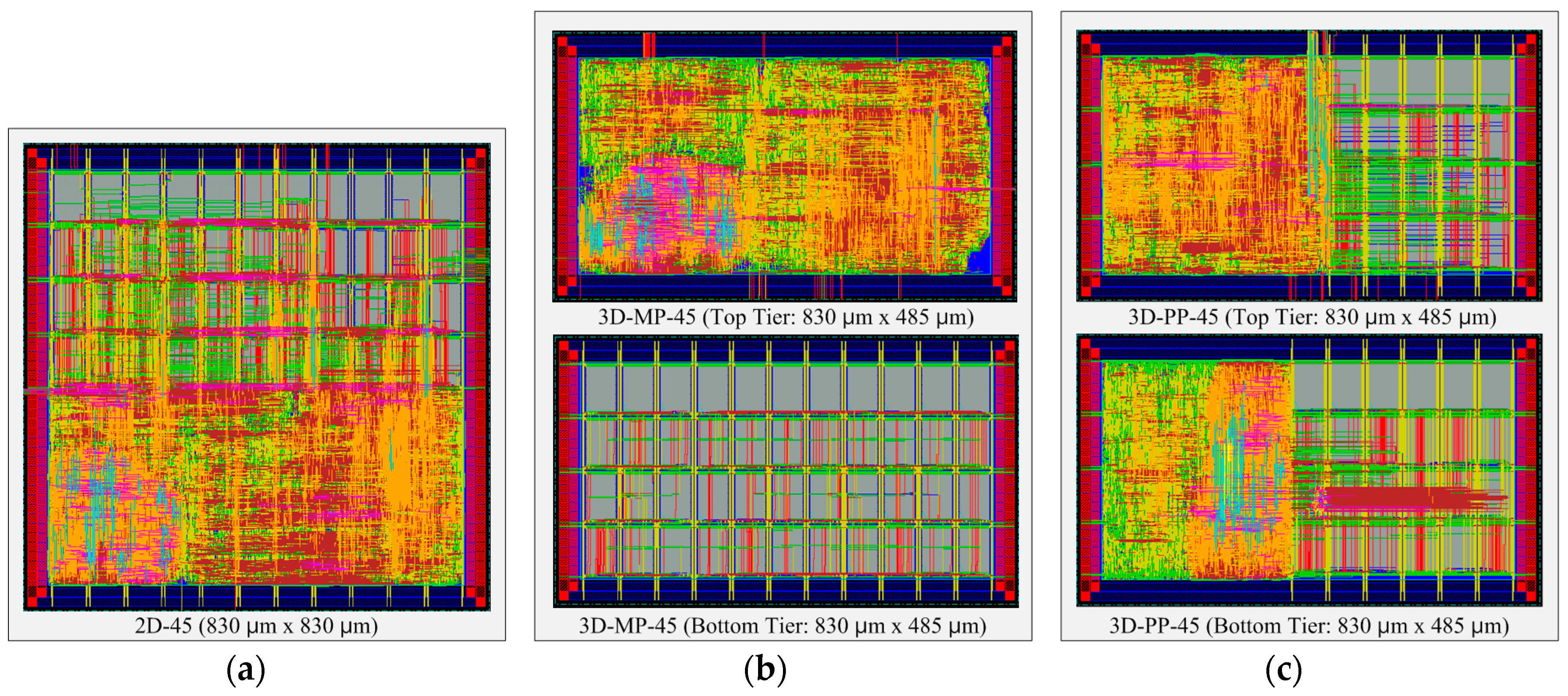
Figure 12.
Layout snapshots of 2D and 3D ICs designed in 45-nm process technology: (a) 2D IC (2D-45); (b) the top and bottom tiers of a 3D IC using macro-level partitioning (3D-MP-45); and (c) the top and bottom tiers of a 3D IC using pipeline-level partitioning (3D-PP-45).
Figure 12.
Layout snapshots of 2D and 3D ICs designed in 45-nm process technology: (a) 2D IC (2D-45); (b) the top and bottom tiers of a 3D IC using macro-level partitioning (3D-MP-45); and (c) the top and bottom tiers of a 3D IC using pipeline-level partitioning (3D-PP-45).
Figure 13.
Normalized power comparisons of 2D and 3D ICs: (a) 130-nm process technology and (b) 45-nm process technology.
Figure 13.
Normalized power comparisons of 2D and 3D ICs: (a) 130-nm process technology and (b) 45-nm process technology.
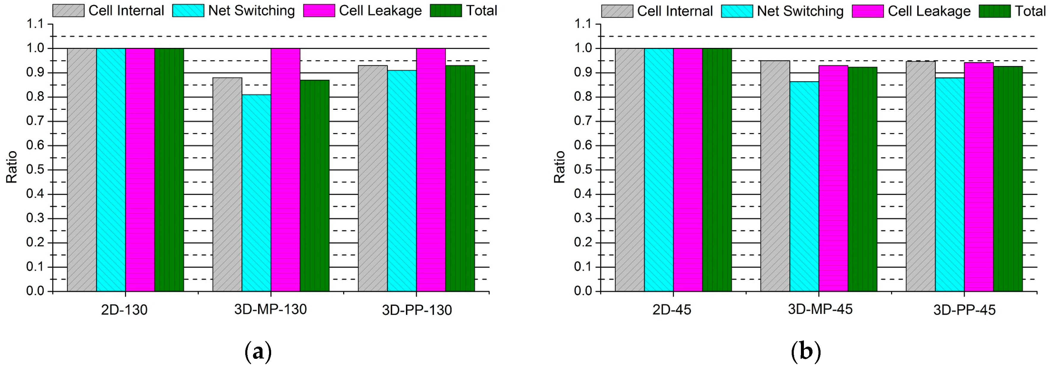
Figure 14.
Normalized power comparisons of 2D and 3D ICs: (a) 130-nm process technology and (b) 45-nm process technology.
Figure 14.
Normalized power comparisons of 2D and 3D ICs: (a) 130-nm process technology and (b) 45-nm process technology.
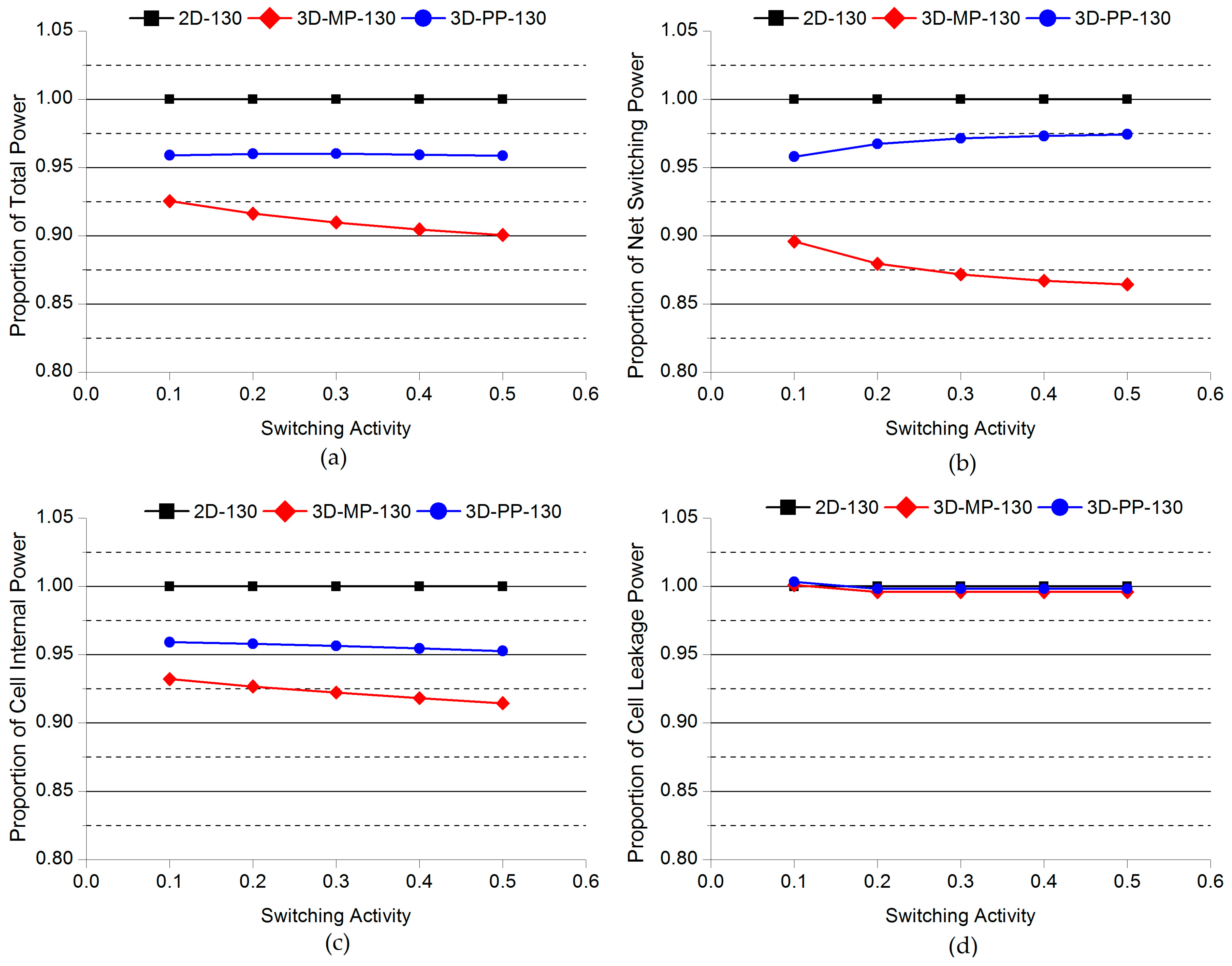
Figure 15.
Comparisons of the normalized power of 2D and 3D ICs as a function of switching activity: (a) Total power; (b) net switching power; (c) cell internal power; (d) cell leakage power. Note that the power consumption of 2D-130 actually increases as the switching activity increases.
Figure 15.
Comparisons of the normalized power of 2D and 3D ICs as a function of switching activity: (a) Total power; (b) net switching power; (c) cell internal power; (d) cell leakage power. Note that the power consumption of 2D-130 actually increases as the switching activity increases.
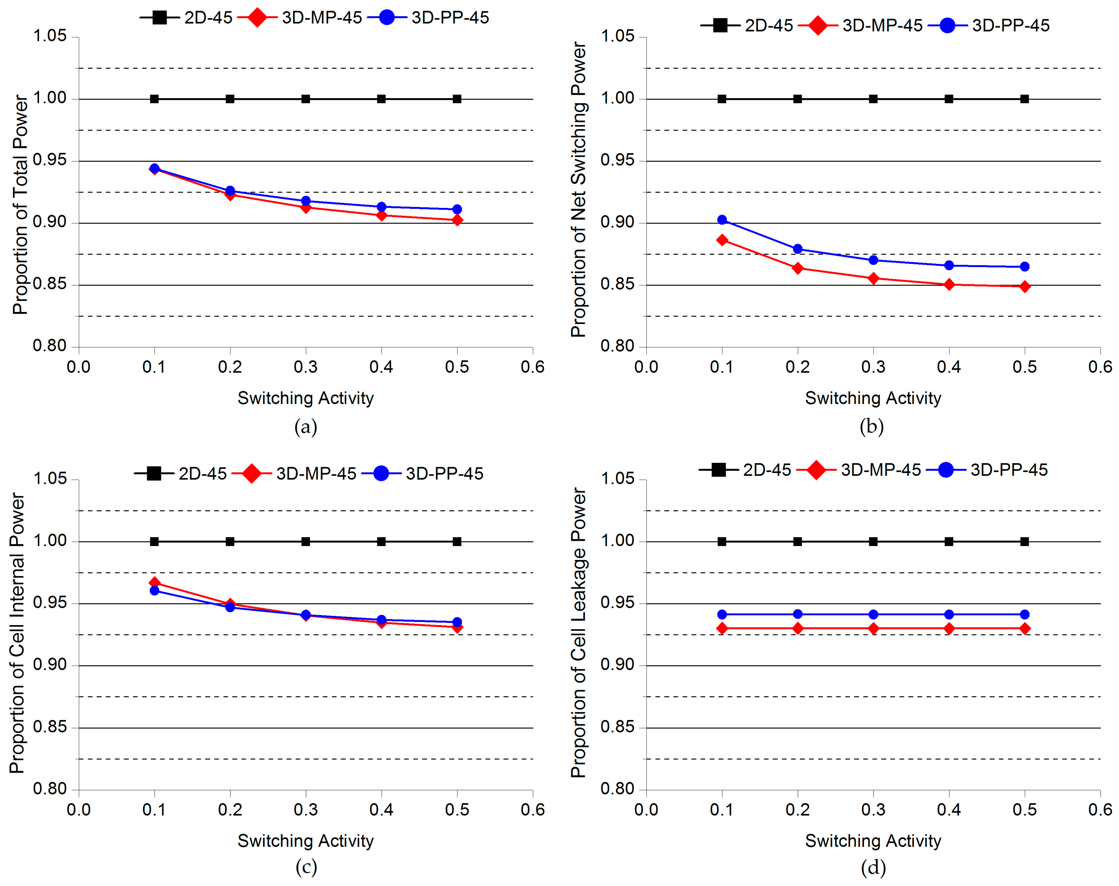
Figure 16.
Comparisons of the normalized power of 2D and 3D ICs as a function of switching activity: (a) Total power; (b) net switching power; (c) cell internal power; (d) cell leakage power. Note that the power consumption of 2D-45 actually increases as the switching activity increases.
Figure 16.
Comparisons of the normalized power of 2D and 3D ICs as a function of switching activity: (a) Total power; (b) net switching power; (c) cell internal power; (d) cell leakage power. Note that the power consumption of 2D-45 actually increases as the switching activity increases.
Table 1.
Related studies on 3D-stacked IC design.
Table 1.
Related studies on 3D-stacked IC design.
| Authors | 3D IC Design | Process Technology | Key Features |
|---|
| Ouyang et al. [7] | Arithmetic units with three logic tiers | Massachusetts Institute of Technology (MIT) Lincoln Lab’s 180 nm | 11.0% ~ 46.1% reduction in power |
| Thorolfsson et al. [8] | FFT processor with two logic tiers and one static random access memory (SRAM) tier | MIT Lincoln Lab’s 180 nm | 56.9% reduction in wire length, 4.4% reduction in logic power |
| Neela et al. [9] | Single precision floating-point unit with two logic tiers | GlobalFoundries 130 nm | 41.5% reduction in footprint, 3% increase in frequency |
| Kim et al. [10] | 64 processors with one logic tier and one SRAM tier | GlobalFoundries 130 nm | 63.8 GB/s memory bandwidth, power consumption up to 4.0 W |
| Zhang et al. [11] | Syntem-on-Chip with two logic tiers and three DRAM tiers | GlobalFoundries 130 nm | 12.57 mW power consumption, 8.5 GB/s bandwidth |
| Saito et al. [12] | Dynamic-reconfigurable memory with one logic tier and one SRAM tier | 90-nm process technology | 63% reduction in area and 43% reduction in latency |
| Franzon et al. [13] | Digital signal processor with two logic tiers and one SRAM tier | MIT Lincoln Lab’s 180 nm | 25% reduction in total power (logic and memory) |
| Oh et al. [14] | Ternary content-addressable memory with three tiers | MIT Lincoln Lab’s 180 nm | 21% reduction in total power |
Table 2.
Main features of our stereo matching processors designed in 130- and 45-nm technologies.
Table 2.
Main features of our stereo matching processors designed in 130- and 45-nm technologies.
| Feature Type | 130-nm Process Technology | 45-nm Process Technology |
|---|
| Maximum frequency | 312 MHz | 556 MHz |
| Image size (pixel) | 752 × 480 | 752 × 480 |
| Window size (pixel) | 15 × 15 | 15 × 15 |
| Disparity range (pixel) | 64 | 64 |
| Maximum frame rate | 108 frames/s | 192 frames/s |
| Maximum bandwidth | 12.8 GB/s | 22.8 GB/s |
Table 3.
Summary of synthesis results.
Table 3.
Summary of synthesis results.
| Process Technology | Area (μm × μm) | Clock Period | # of SRAM | SRAM Capacity |
|---|
| 130-nm | 2,977,542 | 3.2 ns | 44 | 44 × 752 bytes = 31.3 kB |
| 45-nm | 451,797 | 1.8 ns | 44 | 44 × 752 bytes = 31.3 kB |
Table 4.
TSV usage comparisons.
Table 4.
TSV usage comparisons.
| Partition Method | Type of Signal | # of TSVs |
|---|
| Macro-level Partition (MP) | SRAM control signals | 29 |
| SRAM address signals | 20 |
| SRAM data signlas | 376 |
| Total Number of TSVs | 425 |
| Pipeline-level Partition (PP) | Logic signals between pipeline stages | 56 |
| SRAM control signals | 41 |
| SRAM address signals | 20 |
| SRAM data signlas | 104 |
| Total Number of TSVs | 221 |
Table 5.
Cell area of each pipeline stage of the stereo matching processors designed in 130- and 45-nm technologies.
Table 5.
Cell area of each pipeline stage of the stereo matching processors designed in 130- and 45-nm technologies.
| # of Pipeline Stage | Name | 130-nm Process Technology | 45-nm Process Technology |
|---|
| Cell Area (μm × μm) | % | Cell Area (μm × μm) | % |
|---|
| 1 | 32 SRAM macros | 1,294,065 | 43.5 | 194,109 | 43.0 |
| 2 | Hamming weight | 255,783 | 8.6 | 42,660 | 9.4 |
| 3 | Hamming distance | 459,072 | 15.4 | 68,576 | 15.2 |
| 4 | 12 SRAM macros | 485,274 | 16.3 | 72,791 | 16.1 |
| 5 | Median filter | 241,725 | 8.1 | 32,831 | 7.3 |
| 6 | Disparity diffusion | 241,623 | 8.1 | 40,831 | 9.0 |
Table 6.
Overall layout results of 2D and 3D ICs designed in 130-nm process technology.
Table 6.
Overall layout results of 2D and 3D ICs designed in 130-nm process technology.
| | 2D-130 | 3D-MP-130 | 3D-PP-130 |
|---|
| Top Tier | Bottom Tier | Top Tier | Bottom Tier |
|---|
| Clock period (ns) | 3.2 | 3.2 | 3.2 | 3.2 | 3.2 |
| Footprint (μm × μm) | 2350 × 2350 | 2350 × 1350 | 2350 × 1350 | 2350 × 1350 | 2350 × 1350 |
| # of gates | 97,630 | 87,245 | 205 | 50,113 | 39,528 |
| Total wire lengths (μm) | 5,488,514 | 4,507,365 | 220,485 | 2,662,651 | 2,582,875 |
| Clock net wire lengths | 231,232 | 184,683 | 18,293 | 119,704 | 95,636 |
| Total # of buffers | 18,968 | 15,242 | 161 | 8575 | 7051 |
| # of clock tree buffers | 871 | 740 | 61 | 508 | 399 |
| Power (mW) | 1006.31 | 871.04 | 931.30 |
Table 7.
Overall layout results of 2D and 3D ICs designed in 45-nm process technology.
Table 7.
Overall layout results of 2D and 3D ICs designed in 45-nm process technology.
| | 2D-45 | 3D-MP-45 | 3D-PP-45 |
|---|
| Top Tier | Bottom Tier | Top Tier | Bottom Tier |
|---|
| Clock period (ns) | 1.8 | 1.8 | 1.8 | 1.8 | 1.8 |
| Footprint (μm × μm) | 830 × 830 | 830 × 485 | 830 × 485 | 830 × 485 | 830 × 485 |
| # of gates | 123,659 | 101,640 | 165 | 58,745 | 40,859 |
| Total wire lengths (μm) | 1,918,625 | 1,629,674 | 75,494 | 988,637 | 881,191 |
| Clock net wire lengths | 86,758 | 75,249 | 5950 | 47,981 | 38,455 |
| Total # of buffers | 34,520 | 24,198 | 121 | 12,704 | 9863 |
| # of clock tree buffers | 1451 | 1415 | 52 | 909 | 692 |
| Power (mW) | 273.79 | 252.56 | 253.44 |
Table 8.
Detailed power comparisons of 2D and 3D ICs designed in 130-nm technology.
Table 8.
Detailed power comparisons of 2D and 3D ICs designed in 130-nm technology.
| Design Type | Power Group | Cell Internal (mW) | Net Switching (mW) | Cell Leakage (mW) | Total (mW) | Percentage (%) |
|---|
| 2D-130 | Memory | 353.70 | 1.33 | 0.08 | 355.11 | 35.29 |
| Clock Network | 246.10 | 71.0 | 0.00 | 317.10 | 31.51 |
| Register | 41.0 | 14.70 | 0.00 | 55.70 | 5.54 |
| Combinational Logic | 135.80 | 142.60 | 0.00 | 278.40 | 27.67 |
| Total | 776.60 | 229.63 | 0.08 | 1006.31 | 100.0 |
| | Percentage (%) | 77.17 | 22.82 | 0.01 | 100.00 | n/a |
| 3D-MP-130 | Memory | 353.80 | 1.46 | 0.08 | 355.34 | 40.79 |
| Clock Network | 209.70 | 68.20 | 0.00 | 277.90 | 31.90 |
| Register | 31.80 | 12.40 | 0.00 | 44.20 | 5.07 |
| Combinational Logic | 89.80 | 103.80 | 0.00 | 193.60 | 22.23 |
| Total | 685.10 | 185.86 | 0.08 | 871.04 | 100.00 |
| | Percentage (%) | 78.65 | 21.34 | 0.01 | 100.00 | n/a |
| 3D-PP-130 | Memory | 353.70 | 2.02 | 0.08 | 355.80 | 38.20 |
| Clock Network | 219.50 | 68.80 | 0.00 | 288.30 | 30.96 |
| Register | 36.40 | 13.70 | 0.00 | 50.10 | 5.38 |
| Combinational Logic | 113.80 | 123.30 | 0.00 | 237.10 | 25.46 |
| Total | 723.40 | 207.82 | 0.08 | 931.30 | 100.00 |
| | Percentage (%) | 77.68 | 22.32 | 0.01 | 100.00 | n/a |
Table 9.
Detailed power comparisons of 2D and 3D ICs designed in 45-nm technology.
Table 9.
Detailed power comparisons of 2D and 3D ICs designed in 45-nm technology.
| Design Type | Power Group | Cell Internal (mW) | Net Switching (mW) | Cell Leakage (mW) | Total (mW) | Percentage (%) |
|---|
| 2D-45 | Memory | 79.20 | 0.39 | 5.05 | 84.64 | 30.9% |
| Clock Network | 37.30 | 28.10 | 0.13 | 65.53 | 23.9% |
| Register | 15.20 | 5.44 | 0.72 | 21.35 | 7.8% |
| Combinational Logic | 49.90 | 50.40 | 1.97 | 102.27 | 37.4% |
| Total | 181.60 | 84.32 | 7.87 | 273.79 | 1.00 |
| | Percentage (%) | 66.33 | 30.80 | 2.87 | 100.00 | n/a |
| 3D-MP-45 | Memory | 79.2 | 0.4548 | 5.051 | 84.71 | 33.5% |
| Clock Network | 38.4 | 28 | 0.1299 | 66.53 | 26.3% |
| Register | 15.2 | 4.687 | 0.7167 | 20.60 | 8.2% |
| Combinational Logic | 39.6 | 39.7 | 1.419 | 80.72 | 32.0% |
| Total | 172.40 | 72.84 | 7.32 | 252.56 | 100 |
| | Percentage (%) | 68.26 | 28.84 | 2.90 | 100.00 | n/a |
| 3D-PP-45 | Memory | 79.2 | 0.6416 | 5.051 | 84.89 | 33.5% |
| Clock Network | 36.5 | 28.4 | 0.1349 | 65.03 | 25.7% |
| Register | 15.2 | 5.296 | 0.7156 | 21.21 | 8.4% |
| Combinational Logic | 41.1 | 39.7 | 1.505 | 82.31 | 32.5% |
| Total (mW) | 172.00 | 74.04 | 7.41 | 253.44 | 100 |
| | Percentage (%) | 67.87 | 29.21 | 2.92 | 100.00 | n/a |
Table 10.
Comparisons of the power and wire length reductions in this study with those in related studies.
Table 10.
Comparisons of the power and wire length reductions in this study with those in related studies.
| | Power (mW) | Wire Length (m) |
|---|
| 2D IC | 3D IC | ∆ (%) | 2D IC | 3D IC | ∆ (%) |
|---|
| Proposed | 2D-130 | 3D-MP-130 | 1006.3 | 871 | −13.4% | 5.489 | 4.728 | −13.9% |
| 3D-PP-130 | 931.3 | −7.5% | 5.246 | −4.4% |
| 2D-45 | 3D-MP-45 | 273.8 | 252.6 | −7.7% | 1.919 | 1.705 | −11.1% |
| 3D-PP-45 | 253.4 | −7.5% | 1.870 | −2.5% |
| Related Studies | Ouyang et al. [7] | n/a | n/a | n/a | n/a | n/a | n/a |
| Thorolfsson et al. [8] | 340.0 | 324.9 | −4.4% | 19.107 | 8.238 | −56.9% |
| Neela et al. [9] | 9.95 | 10.72 | 7.7% | 10.37 | 10.96 | 5.7% |
| Kim et al. [10] | n/a | 4032.0 | n/a | n/a | n/a | n/a |
| Zhang et al. [11] | n/a | 12.57 | n/a | n/a | n/a | n/a |
| Saito et al. [12] | n/a | 120.0 | n/a | n/a | n/a | n/a |
| Franzon et al. [13] | 340.0 | 324.9 | −4.4% | 19.107 | 8.238 | −56.9% |
| Oh et al. [14] | 0.042 | 0.033 | −21.5% | n/a | n/a | n/a |


