1. Introduction
High image quality in low light conditions is highly appreciated in many applications, such as security, surveillance, automotive, and IPC applications, to name a few. On the other hand, high sensitivity to low-light objects is also required in these applications. In low light conditions, image sensors are usually operated in a high gain mode, and image quality suffers from low signal saturation due to the limited dynamic range. Many approaches have been introduced in order to expand the image sensor dynamic range while keeping low light image quality, including multiple exposure [
1,
2,
3,
4], logarithmic compression [
5,
6], knee compression [
7], multiple column gain readout [
8], and more [
9,
10].
Among these approaches, the multiple exposure high dynamic range (MEHDR) approach is the most common scheme, where images with different exposure times are captured and then merged into a high dynamic range image. Line interleave exposure control or pixel interleave exposure control schemes are also included in this category. However, this approach has fundamental issues associated with the different exposure timings for long exposures and for short exposures, which can generate artifacts against moving objects or time-varying light sources like pulsed LEDs. Another issue is SNR degradation at the conjunction point of the two images. To suppress the artifacts from the pulsed LEDs, chopping integration has been introduced [
11]. However, even with the chopping integration, the SNR drop at the conjunction point is still an issue.
The second major approach uses two kinds of pixel—one with lower sensitivity, and the other with higher sensitivity—implemented in the same pixel array, and the different sensitivity signals combined into a linear signal [
12]. This approach needs redundant pixels. Also, it needs careful optical design to obtain uniform optical performance of angular dependence, cross-talk and spectral response between the two kinds of pixels.
An ideal solution is to expand pixel saturation while keeping high sensitivity in low light conditions. The lateral overflow integration capacitor (LOFIC) approach is considered to be one of these solutions, with a high dynamic range of more than 100 dB having been demonstrated in a single exposure [
13,
14]. On the other hand, LOFIC needs a charge accumulation node outside the photodiode. Reduction of junction leakage and defect control of the charge accumulation node are challenging issues in terms of manufacturability.
The basis of the dynamic range enhancement introduced in this image sensor is a dual gain readout scheme [
15], and follows the following sequence: (1) a photodiode signal is read out in a high gain mode, and (2) read out in a low gain mode; then, (3) the two signals are merged into a high dynamic range linear signal. The intra-scene dynamic range in this scheme is defined as the ratio between linear full well (LFW) to readout noise in the high gain condition. Therefore, increase of the LFW and reduction of readout noise floor are required to increase dynamic range.
In this paper, we present a 3 μm, high dynamic range pixel, using a multiple-junction photodiode and a triple-conversion gain configuration [
16] in
Section 2. The high gain conversion of the pixel is able to detect small signals in low light conditions with a low readout noise, while low gain conversion covers a large LFW of 40 ke
−. In
Section 3, the architecture of the image sensor and pixel operation sequence are described, followed by the characterization results [
17] in
Section 4, and conclusions in
Section 5.
2. The Triple-Conversion Gain Pixel
In this section, pixel configuration, photodiode design and operation sequence of the triple-conversion gain pixel are described.
2.1. Pixel Configuration
Electron-referred readout noise can be reduced by increasing pixel conversion gain. However, higher pixel conversion gain results in lower signal saturation, because of the limited voltage window of the charge detection node.
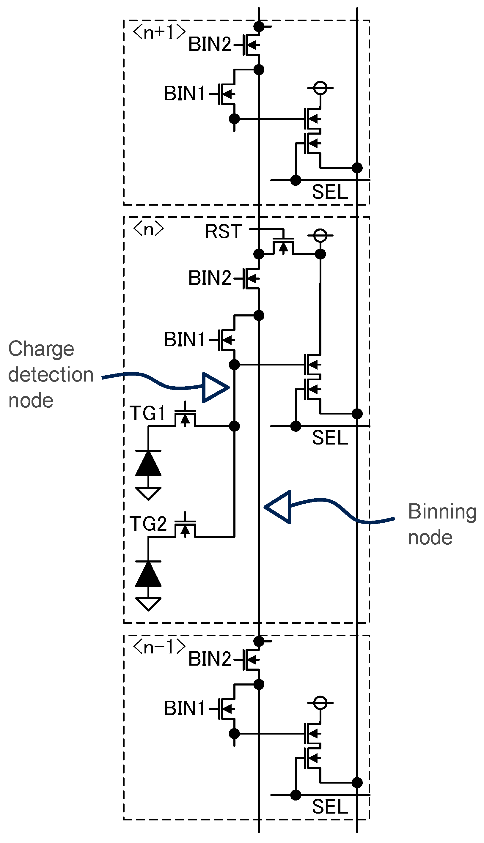
The developed 3.0 μm pixel configuration is shown in
Figure 1. The pixel has a two row-shared structure. Through switches, BIN1 and BIN2, the charge detection node is vertically connected. These binning switches act as vertical binning switches. To prevent extra parasitic capacitance when high pixel gain is required, the charge detection node is isolated from the vertical binning node by the BIN1 switch.
The BIN1 and the BIN2 switches are utilized not only for the binning purpose, but also for pixel gain control. When the BIN1 switch is closed during the pixel readout, the gate capacitance of the BIN1 switch and metal capacitance of the vertical binning line serve as an additional capacitance of the charge detection node and thus reduce the pixel gain. Closing the BIN2 switch additionally, more capacitance is added to the charge detection node. Thus, by controlling the BIN1 and the BIN2 switches, three different conversion gains can be obtained without additional devices like a poly-insulator-poly (PIP) capacitor or a metal-insulator-metal (MIM) capacitor, which is used in the conventional dual-conversion gain pixel architecture [
18].
2.2. Dual Gain Readout Sequence
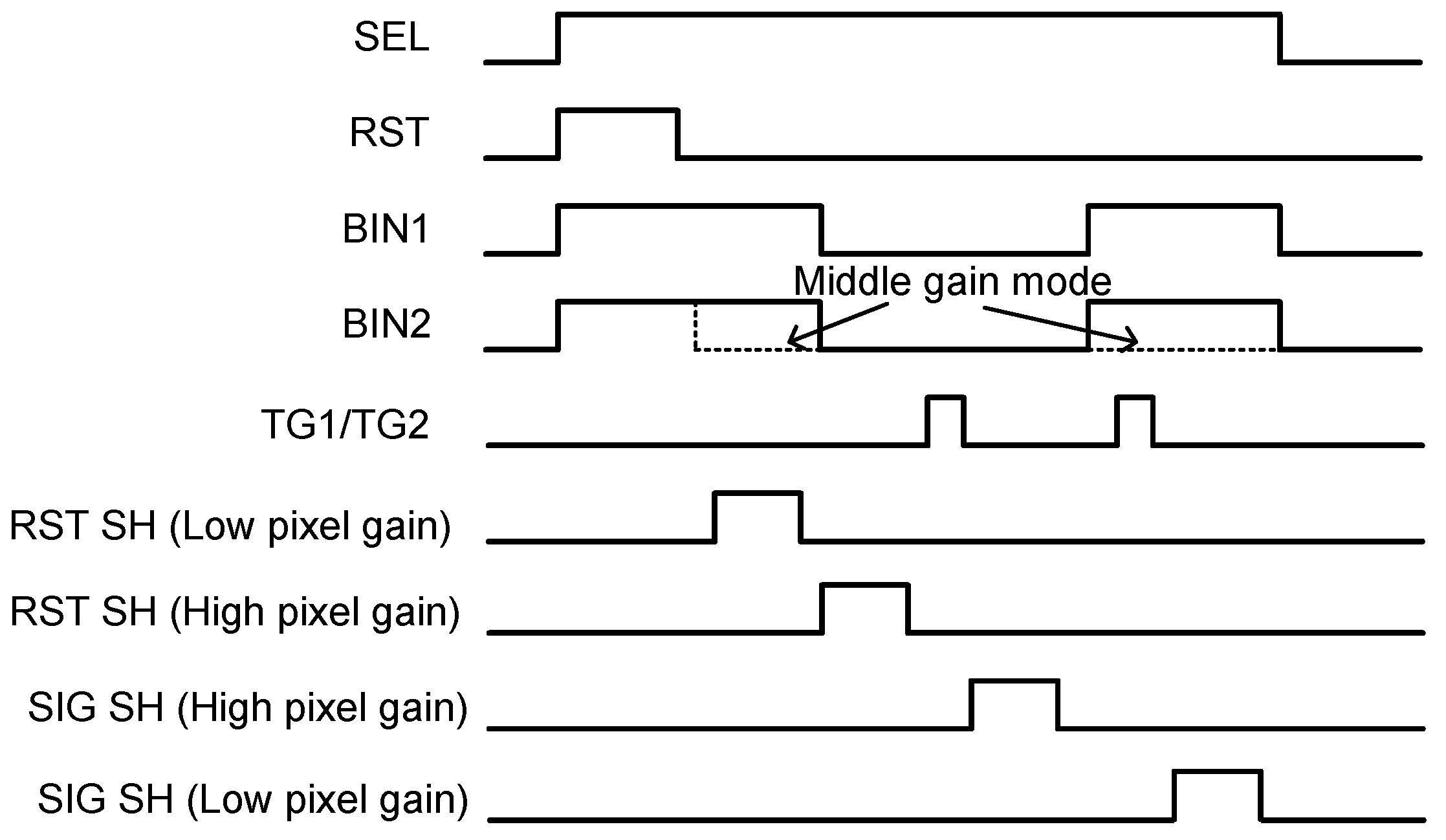
To obtain a linearized high dynamic range signal, the same photodiode signal is read out twice with different pixel gains.
Figure 2 shows a pixel operation timing for the dual pixel gain readout. Firstly, RST, BIN1 and BIN2 switches are all turned on to initialize voltage of the vertical binning node and the charge detection node. After the RST switch is turned off, a low pixel gain (LPG) offset signal is sampled as RST SH (Low pixel gain). Next, BIN1 and BIN2 switches are turned off, and high pixel gain (HPG) offset, RST (High pixel gain) is sampled. A first charge transfer pulse is applied on the transfer gate, TG; then, the HPG signal, SIG SH (High pixel gain) is sampled. LPG signal is obtained after BIN1 and BIN2 are turned on again, and sampled as SIG SH (Low pixel gain). Before the LPG signal readout, the second transfer pulse is applied to the TG gate so that remaining charge in the photodiode is transferred to the charge detection node in case of high light conditions. When BIN1 and BIN2 switches are turned on again, offset charge in the charge detection node is re-combined to the same condition as the RST SH (Low pixel gain); therefore, correlated double sampling (CDS) is realized for LPG signal readout as well as the HPG. When the BIN2 switch is turned off (dotted line in
Figure 2) during the signal readout period, the pixel operates in the middle pixel gain (MPG) condition.
2.3. High Linear Full Well (LFW) Photodiode
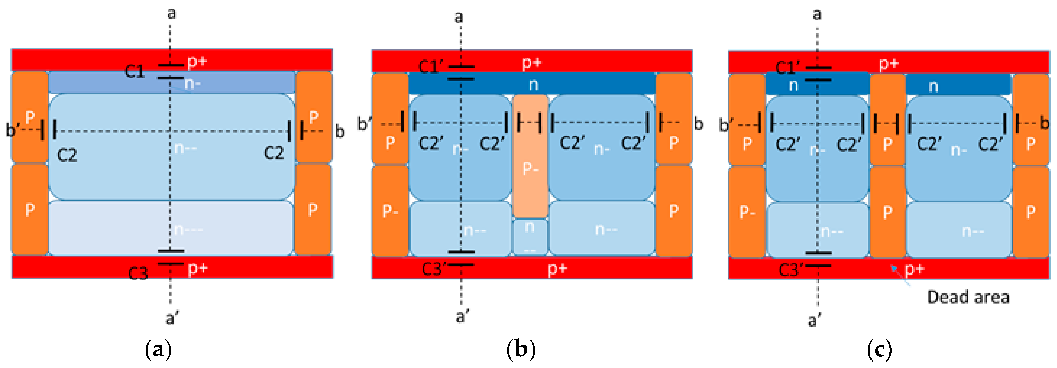
A conventional pinned photodiode (PPD [
19]) structure, the proposed photodiode structure and a conventional split-pinned diode structure are shown in
Figure 3a–c, respectively. In the presented structure,
Figure 3b, a P-type layer is formed in the center of PPD, like a P-type pixel isolation layer. Because of the narrow photodiode effect, the split photodiode structure is effective for maintaining a low
Vpin when the LFWC is increased by additional dosage for the N-type photodiode. The conventional split photodiode structure [
20], which has 2 sets of PPDs and a transfer gate and one floating diffusion node per pixel, is shown in
Figure 3c for comparison. The stratified PPD structure [
21], which has vertically stacked P-type layers, is considered a reference of this type of PPD structure.
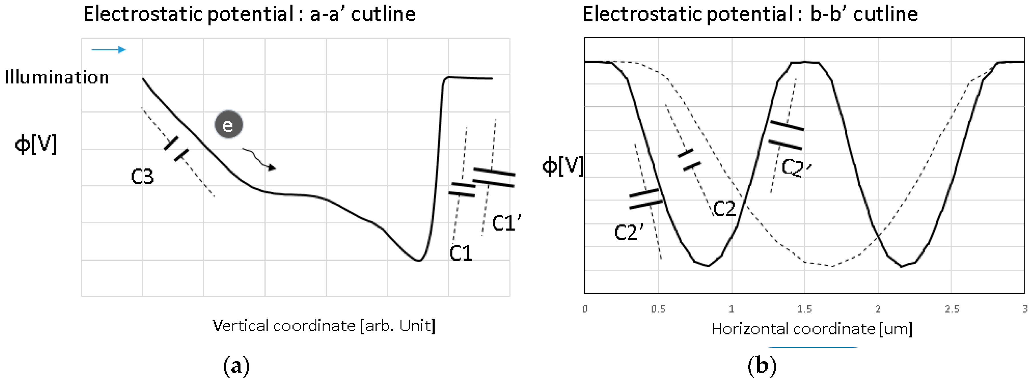
Figure 4 shows an example of electrostatic potential profiles with capacitance components along the lines of
Figure 4a a-a’ and
Figure 4b b-b’ in
Figure 3a for both the conventional PPD and the presented one. In the simple P
+/N step junction model, the depletion layer width
Wd in PPD is expressed as Equation (1), where ε is the semiconductor dielectric constant,
Vpin the pinning voltage when the PPD is fully depleted,
Nd the
N dopant concertation, and
φbi the built-in potential.
Equation (1) suggests that the
Wd (fully depleted region) becomes narrower in the presented structure in
Figure 3b due to the additional P-type layer between the split PPDs. Thus, the
Vpin to fully deplete the PPD can be lower than for the conventional structure shown in
Figure 3a, even with the same
N dopant,
Nd. This means that the proposed structure allows
Nd to be increased in order to boost LFWC with the same
Vpin as that of the conventional PPD.
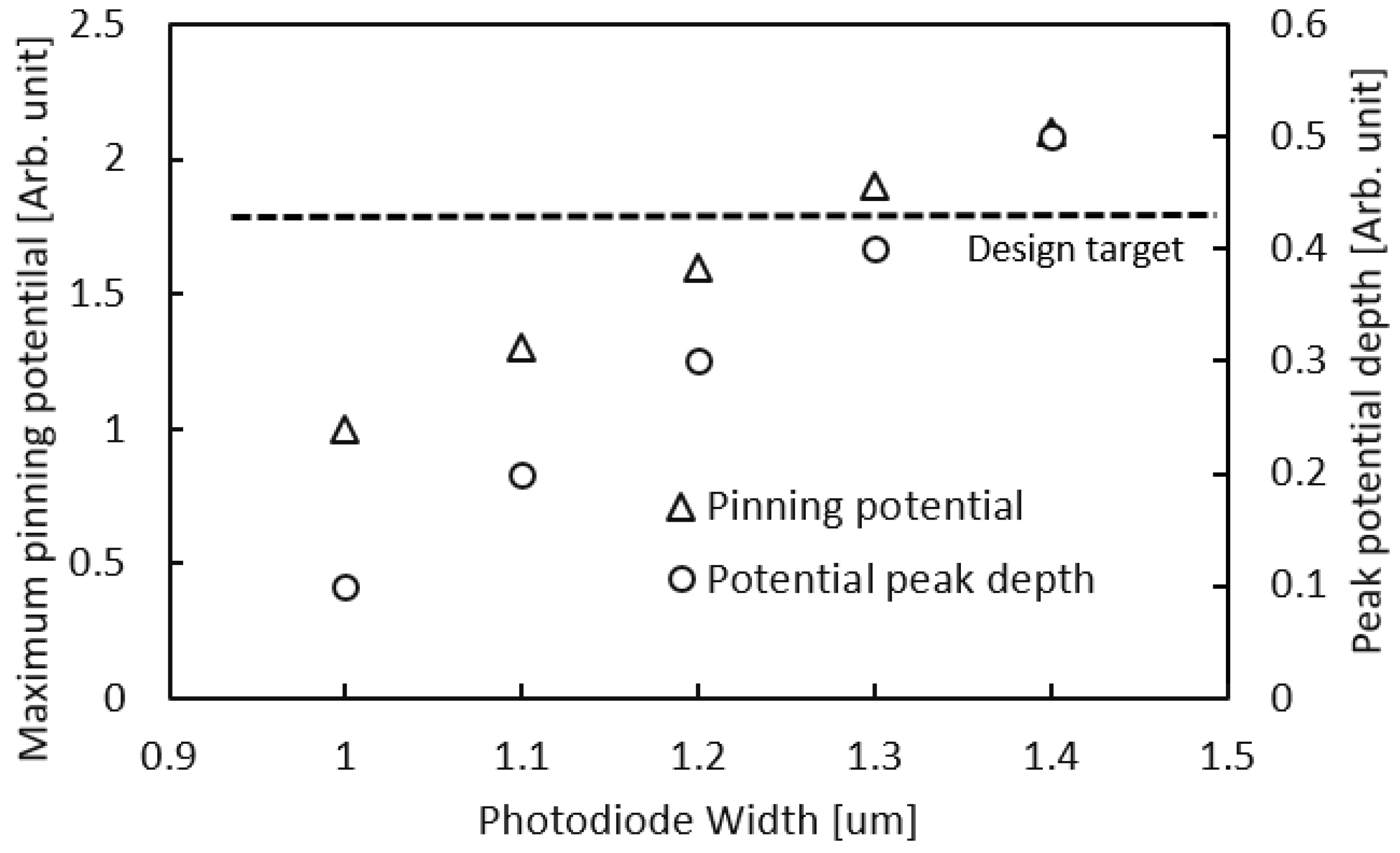
Figure 5 shows the PPD width dependence of the pinned potential and the peak potential depth, as obtained by a 2D device simulation. The results show that the location of the potential peak shifts deeper and the peak potential increases as the PPD width is increased. This suggests that it is difficult to boost LFWC with a large PPD by increasing the
N dopant without changing
Vpin or supplying voltage. This is a benefit of the presented PPD structure, which only uses a narrow PPD width.
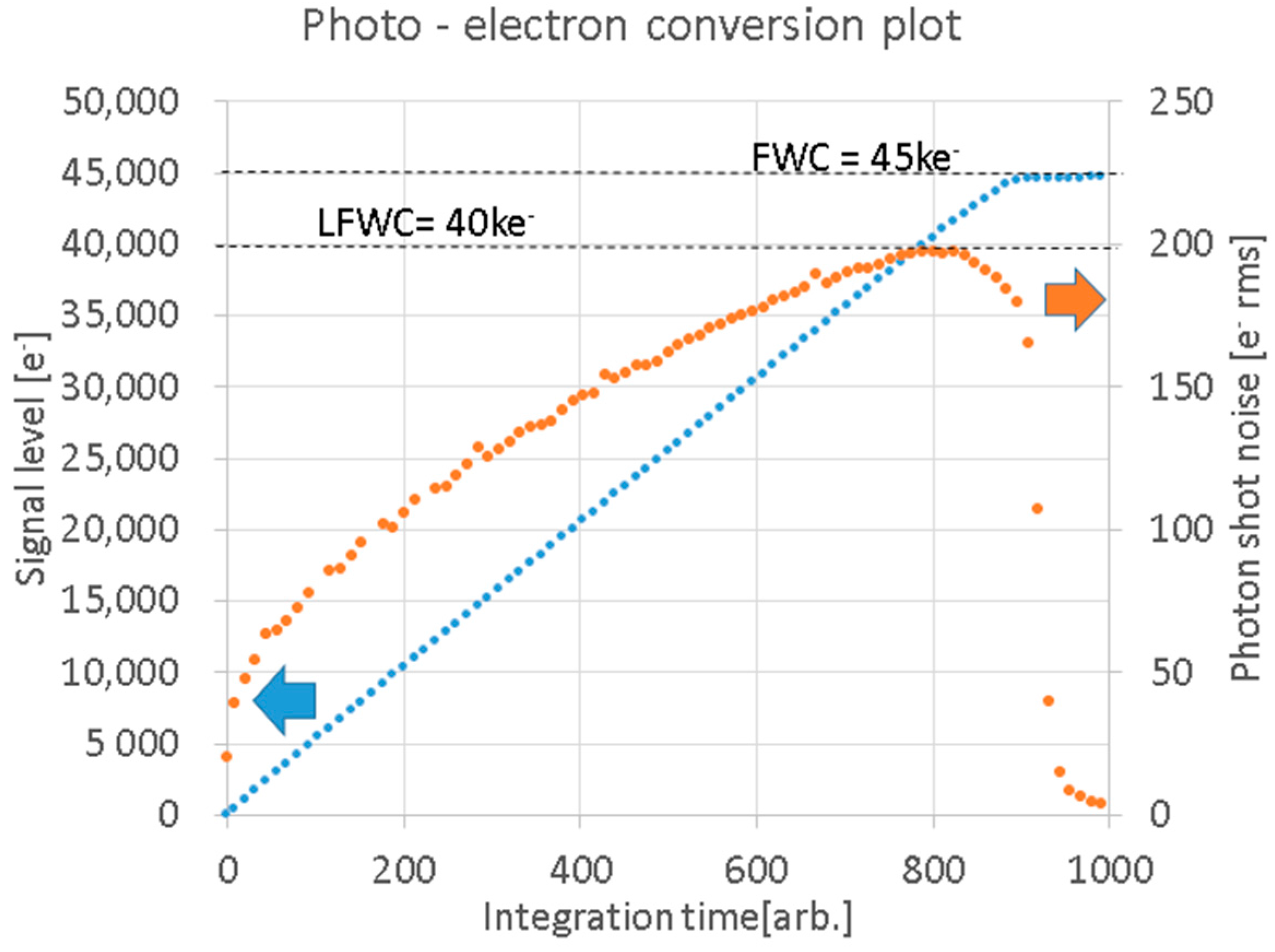
A photo-electron conversion plot for this pixel is shown in
Figure 6. A linear full well capacity (LFWC) of 40 ke
− and a full well capacity (FWC) of 45 ke
− were obtained with good linearity. In this paper, LFWC is defined as signal electrons measured at the shot noise peak point. Above LFWC, random noise decreases because of pixel saturation. Also, FWC is defined as signal electrons corresponding to PD saturation.
3. Sensor Architecture
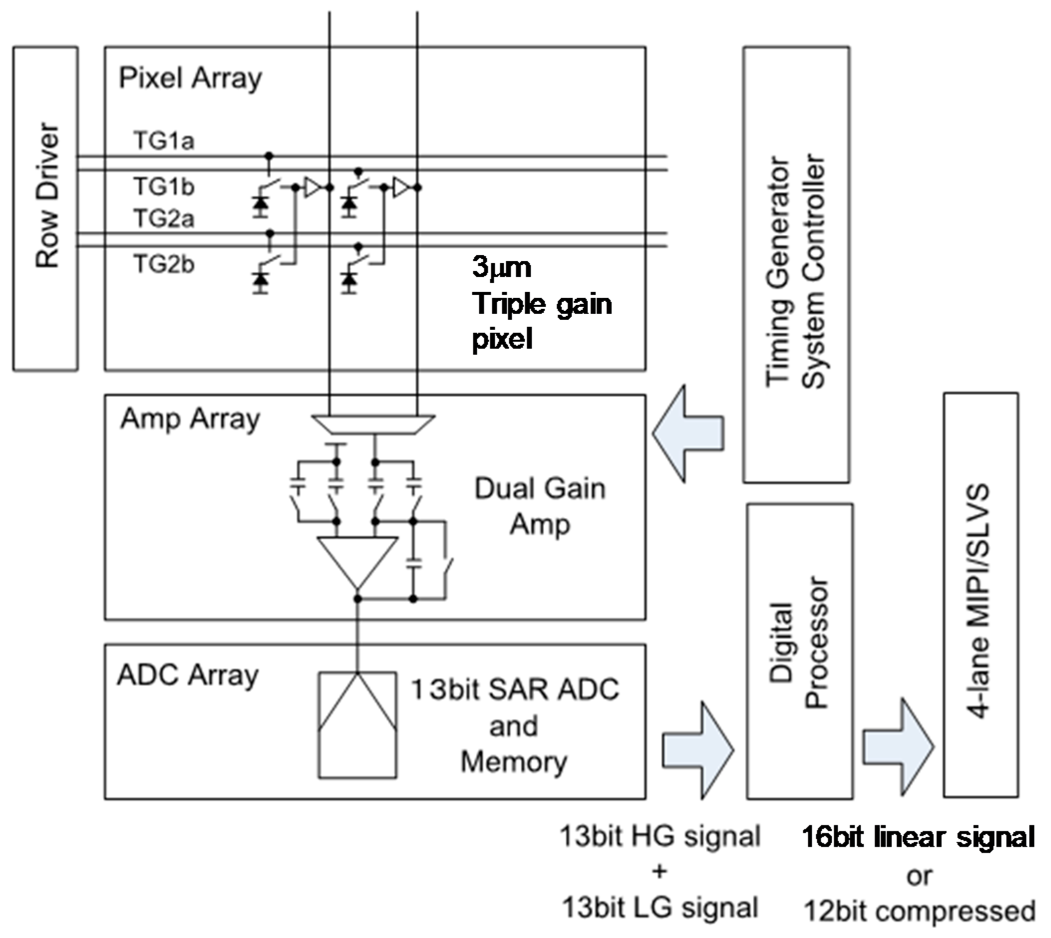
Top architecture of the image sensor is shown in
Figure 7. Odd column pixels and even column pixels have individual TG control lines TG1a/TG1b and TG2a/TG2b, so that even and odd column pixels are read out serially, which allows us to assign one signal chain for two pixel columns.
The column signal chain consists of an amplifier array, a 13 bit successive approximation register (SAR) ADC array and column memory. The column amplifier has two separated signal input paths, which enables two independent CDS operations with different gains. In combination with the multiple-gain pixel and the dual-gain column amplifier, flexible control with a wide gain ratio is available. For the LPG readout, an amplifier gain of either 1× or 2× can be chosen, and for the HPG readout, amplifier gains of 1×, 2×, 4×, 8× are selectable.
After A/D conversion, the two sets of signals are fed to an on-chip digital processor, yielding a high dynamic range 16 bit linear signal. Finally, the 16 bit linear signals or compressed 12 bit signals are output through 4-lane MIPI or SLVS interface. The image sensor is capable of operating at 120 fps in a normal signal readout mode, or 60 fps in the SEHDR mode.
4. Fabrication and Characterization Results
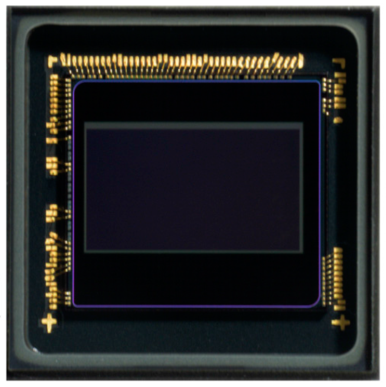
The sensor is fabricated in a 65 nm BSI CMOS image sensor process, and assembled in a 48-pin PLCC package as shown in
Figure 8.
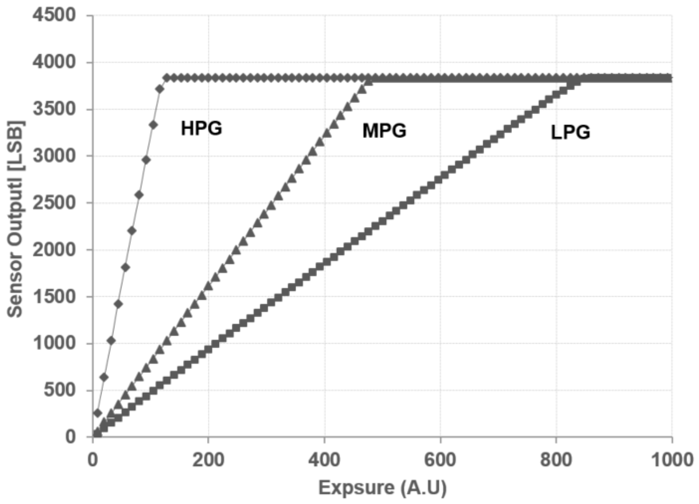
Photo conversion characteristics in the normal mode are shown in
Figure 9. Pixel conversion gains in the HPG condition, the MPG condition and the LPG condition were measured as 152 μV/e
−, 38 μV/e
− and 21 μV/e
−, respectively. Using the MPG as reference for a base pixel gain, the pixel gain ratio is 4.0:1:0.57.
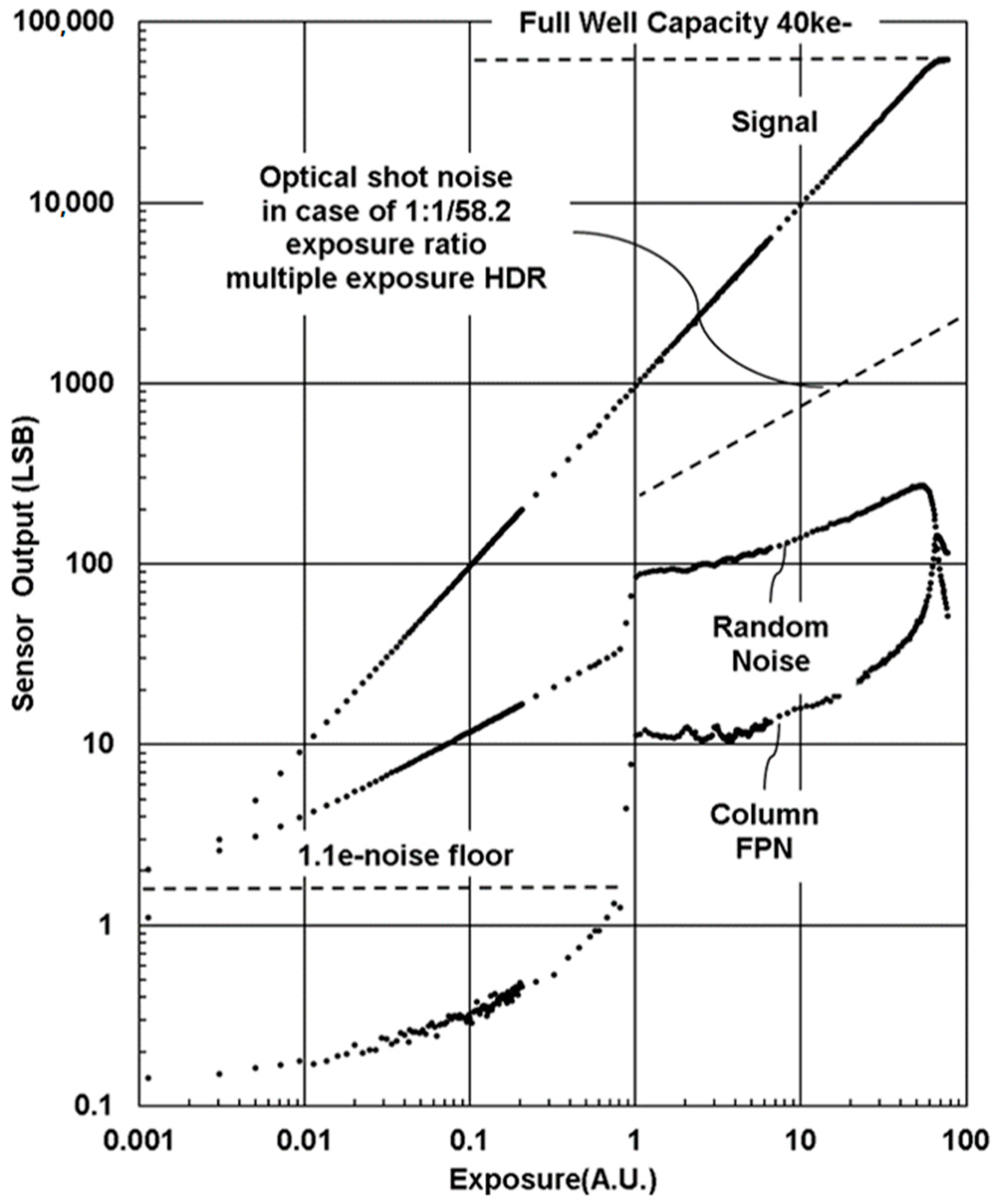
Figure 10 shows an example of photo conversion characteristics obtained under the SEHDR mode with a gain setting of [LPG + Analog gain of 1×]/[HPG + Analog gain of 8×]. Effective gain ratio between the two signals is about 1:58.2. Dark noise floor in the SEHDR mode is identical to the noise at the highest gain setting of 1.1 e
−. The ADC window was set at 40 ke
−, so that maximum dynamic range of 91 dB was obtained. The number of signal electrons at the conjunction point of the HPG signal and the LPG signal was about 800 e
−.
The signal exhibits linear characteristics in the whole range from lower than 1e− to the saturation level, suggesting that the charge transfer error from the photodiode to the charge detection node is smaller than 1 e−, and therefore that the sensor shows excellent low light linearity.
Random noise, pixel FPN and column FPN are also plotted in
Figure 10. Column FPN in low exposure conditions is lower than 1/20 of the random noise, and one can hardly see it. When the amplifier gain is changed at the conjunction point, excess noise and excess FPN are generated due to its circuit operation, and the excess random noise affects SNR by −8 dB. Except for the excess noise, random noise characteristics follow the shot noise model of ∝
S−0.5 throughout the whole range, where S is averaged signal. In comparison to the MEHDR scheme, no significant noise at the conjunction point is seen. When we suppose 1:1/32 integration time ratio in the MEHDR scheme, shot noise degrades about 15 dB at the conjunction point as illustrated by the dotted line in the figure. This is one of benefits of the SEHDR scheme, because no signal charges are lost.
The photo response non-uniformity (PRNU) of the sensor is lower than 0.5%, which suggests that the process variations of the gate capacitance and parasitic metal capacitance are small enough to be used for pixel capacitance.
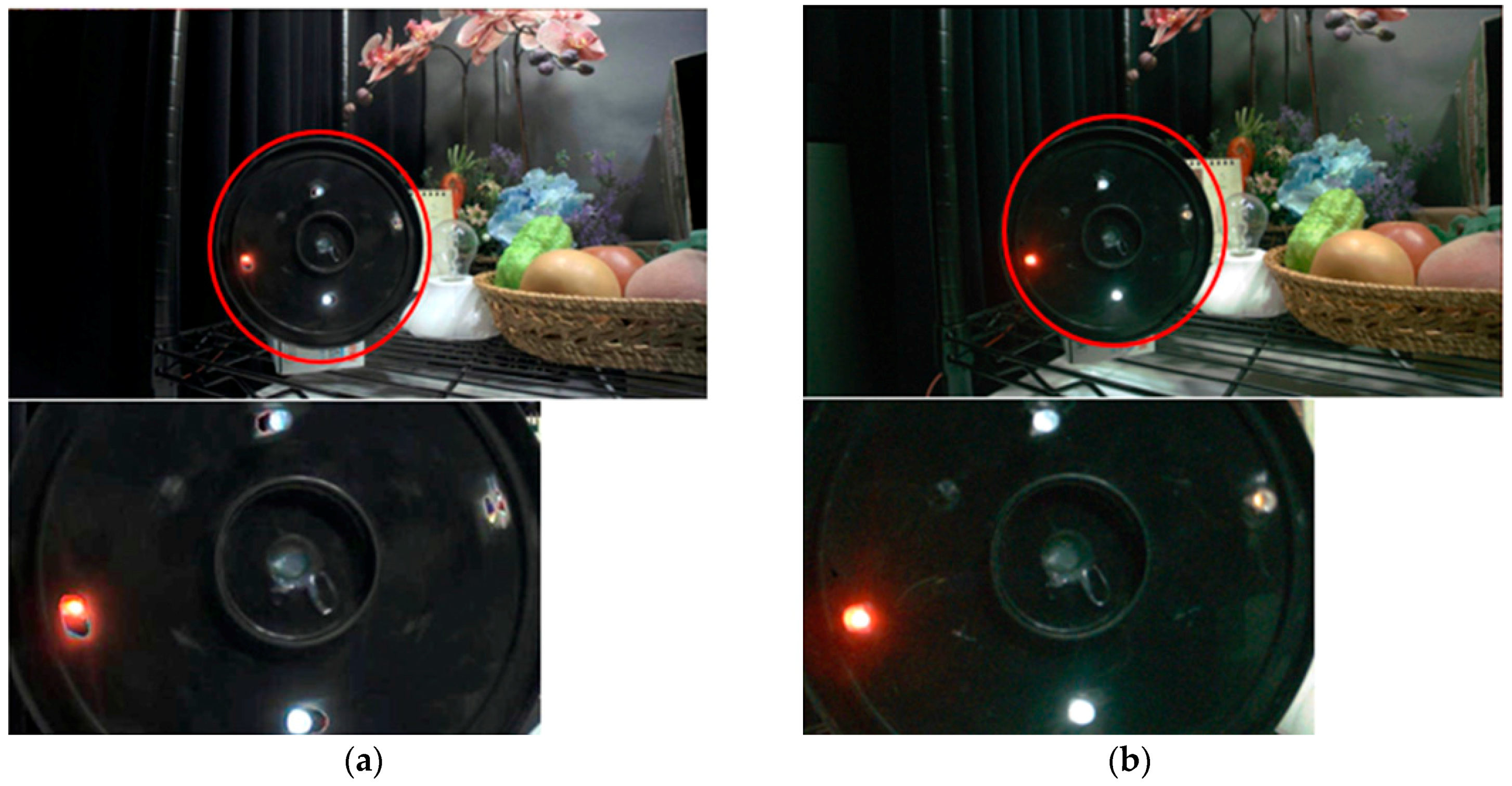
Figure 11a,b shows images captured in the conventional MEHDR mode and in the SEHDR mode reported in this paper, respectively. Motion artifacts and LED flicker artifacts are clearly suppressed in the single-exposure image.
5. Conclusions
An image sensor that has an SEHDR feature was reported. By introducing a triple-conversion gain pixel and a dual-gain readout scheme, the sensor is able to cover an intra-scene dynamic range wider than 87 dB in MPG + HCG mode, and 91 dB in LPG + HCG mode. Because of there being no signal loss in high light conditions, there is no significant SNR drop at the conjunction point. In addition, the SEHDR scheme mitigates moving artifacts or flicker artifact in high dynamic range image applications. Specs and performance are summarized in
Table 1.
Author Contributions
Isao Takayanagi convinced first generation architecture, supervised whole design of the device and wrote manuscript. Norio Yoshimura managed overall design project, created analog architecture and designed analog circuit. Kazuya Mori conceived the photodiode architecture, handled device simulation and pixel characterization, and wrote manuscript of the pixel part. Shinichiro Matsuo led overall logic design tasks including timing definition, module definition, digital top architecture and design verification. Shunsuke Tanaka handled process design and optical design. Hirofumi Abe supervised top level layout and package design. Naoto Yasuda integrated analog layout, and handled layout verification. Kenichiro Ishikawa handled sensor characterization, analysis and basic data acquisition. Shunsuke Okura conceived pixel configuration and operation schemes. Shinji Ohsawa supervised overall characterization, debug, analysis, and data acquisition for the manuscript. Toshinori Otaka analyzed SEHDR performance and optimized pixel operating condition.
Conflicts of Interest
The authors declare no conflict of interest.
References
- Komobuchi, H.; Fukumoto, A.; Yamada, T.; Matsuda, Y.; Kuroda, T. 1/4 inch NTSC format hyper-D range IL-CCD. In Proceedings of the IEEE Workshop on CCDs and Advanced Image Sensors, Dana Point, CA, USA, 20–22 April 1995. [Google Scholar]
- Nakamura, T.; Saitoh, K. Recent progress of CMD imaging. In Proceedings of the IEEE Workshop on CCDs and Advanced Image Sensors, Bruges, Belgium, 5–7 June 1997. [Google Scholar]
- Yadit-Pecht, O.; Fossum, E.R. Wide intrascene dynamic range CMOS APS using dual sampling. IEEE Trans. Electron Devices 1997, 44, 1721–1723. [Google Scholar] [CrossRef]
- Mase, M.; Kawahito, S.; Sasaki, M.; Wakamori, Y.; Furuta, M. A wide dynamic range CMOS image sensor with multiple exposure-time signal outputs and 12-bit column-parallel cyclic A/D converters. IEEE J. Solid-State Circuits 2005, 40, 2787–2795. [Google Scholar] [CrossRef]
- Chamberlain, S.G.; Lee, J.P.Y. A novel wide dynamic range silicon photodetector and linear imaging array. IEEE Trans. Electron Devices 1984, 31, 175–182. [Google Scholar] [CrossRef]
- Scheffer, D.; Dierickx, B.; Meynants, G. Random addressable 2048 × 2048 active pixel image sensor. IEEE Trans. Electron Devices 1997, 44, 1716–1720. [Google Scholar] [CrossRef]
- Decker, S.; McGrath, D.; Brehmer, K.; Sodini, C.G. A 256 × 256 CMOS imaging array with wide dynamic range pixels and column-parallel digital output. IEEE J. Solid-State Circuits 1998, 33, 2081–2091. [Google Scholar] [CrossRef]
- Fowler, B.; Liu, C.; Mims, S.; Balicki, J.; Li, W.; Do, H.; Vu, P. Wide dynamic range low light level CMOS image sensor. In Proceedings of the International Image Sensor Workshop, Bergen, Norway, 26–28 June 2009. [Google Scholar]
- Guilvard, A.; Magnan, P.; Segura, J.; Gonthier, P.M. A high dynamic range digital LinLog CMOS image sensor architecture based on event readout of pixels and suitable for low voltage operation. In Proceedings of the International Image Sensor Workshop, Ogunquit, ME, USA, 7–10 June 2007. [Google Scholar]
- Ando, F.; Shimamoto, H.; Fujita, Y. A digital pixel image sensor with 1-bit ADC and 8-bit pulse counter in each pixel. IEEE Trans. Electron Devices 2000, 47, 2123–2127. [Google Scholar]
- Silsby, C.; Velichko, S.; Johnson, S.; Lim, Y.P.; Mentzer, R.; Beck, J. A 1.2 MP 1/3” CMOS image sensor with light flicker mitigation. In Proceedings of the International Image Sensor Workshop, Vaals, The Netherlands, 8–11 June 2015. [Google Scholar]
- Willassen, T.; Solhusvik, J.; Johansson, R.; Yaghmai, S.; Rhodes, H.; Manabe, S.; Mao, D.; Lin, Z.; Yang, D.; Cellek, O.; et al. A 1280 × 1080 4.2 μm split-diode pixel HDR sensor in 110 nm BSI CMOS process. In Proceedings of the International Image Sensor Workshop, Vaals, The Netherlands, 8–11 June 2015. [Google Scholar]
- Akahane, N.; Sugawa, S.; Adachi, S.; Mori, K.; Ishiuchi, T.; Mizobuchi, K. A sensitivity and linearity improvement of a 100-dB dynamic range CMOS image sensor using a lateral overflow integration capacitor. IEEE J. Solid-State Circuits 2006, 41, 851–858. [Google Scholar] [CrossRef]
- Wakashima, W.; Kusuhara, F.; Kuroda, R.; Sugawa, S. A linear response single exposure CMOS image sensor with 0.5 e− readout noise and 76 ke− full well capacity. In Proceedings of the Symposium on VLSI Circuits (VLSI Circuits), Kyoto, Japan, 17–19 June 2015; pp. C88–C89. [Google Scholar]
- Wang, X.; Wolfs, B.; Meynants, G.; Bogaerts, J. An 89 dB dynamic range CMOS image sensor with dual transfer gate pixel. In Proceedings of the International Image Sensor Workshop, Hokkaido, Japan, 8–11 June 2011. [Google Scholar]
- Mori, K.; Okura, S.; Hasegawa, T.; Tanaka, S.; Takayanagi, I. Back side illuminated high dynamic range 3.0 μm pixel featuring vertical p-n junction capacitance in a deep pinned photodiode. In Proceedings of the International Image Sensor Workshop, Hiroshima, Japan, 30 May–2 June 2017. [Google Scholar]
- Takayanagi, I.; Yoshimura, N.; Mori, K.; Tanaka, S.; Matsuo, S.; Abe, H.; Yasuda, N.; Ishikawa, K.; Okura, S.; Ohsawa, S.; et al. An 87 dB single exposure dynamic range CMOS image sensor with a 3.0 µm triple conversion gain pixel. In Proceedings of the International Image Sensor Workshop, Hiroshima, Japan, 30 May–2 June 2017. [Google Scholar]
- Huggett, A.R.; Chris, S.; Sergi, C. A dual-conversion-gain video sensor with dewarping and overlay on a single chip. In Proceedings of the IEEE International Solid-State Circuits Conference—Digest of Technical Papers, San Francisco, CA, USA, 8–12 February 2009; pp. 52–53. [Google Scholar]
- Teranishi, N. Effect and limitation of pinned photodiode. IEEE Trans. Electron Devices 2016, 63, 10–15. [Google Scholar] [CrossRef]
- Kobayashi, M.; Johnson, M.; Wada, Y.; Tsuboi, H.; Ono, T.; Takada, H.; Togo, K.; Kishi, T.; Takahashi, H.; Ichikawa, T.; et al. A low noise and high sensitivity image sensor with imaging and phase-difference detection AF in all pixels. In Proceedings of the International Image Sensor Workshop, Vaals, The Netherlands, 8–11 June 2015. [Google Scholar]
- Lim, Y.; Lee, K.; Hong, H.; Kim, J.; Sa, S.; Lee, J.; Kim, D.; Hynecek, J. Stratified photodiode a new concept for small size-high performance CMOS image sensor pixels. In Proceedings of the International Image Sensor Workshop, Ogunquit, ME, USA, 7–10 June 2007. [Google Scholar]
© 2018 by the authors. Licensee MDPI, Basel, Switzerland. This article is an open access article distributed under the terms and conditions of the Creative Commons Attribution (CC BY) license (http://creativecommons.org/licenses/by/4.0/).


