Experimental Characterization of Inkjet-Printed Stretchable Circuits for Wearable Sensor Applications


Abstract
:1. Introduction
2. Materials and Methods
2.1. Materials and Equipment
2.1.1. Preparation of PDMS Substrate
2.1.2. Inkjet Printing
2.1.3. Electrical Interconnects
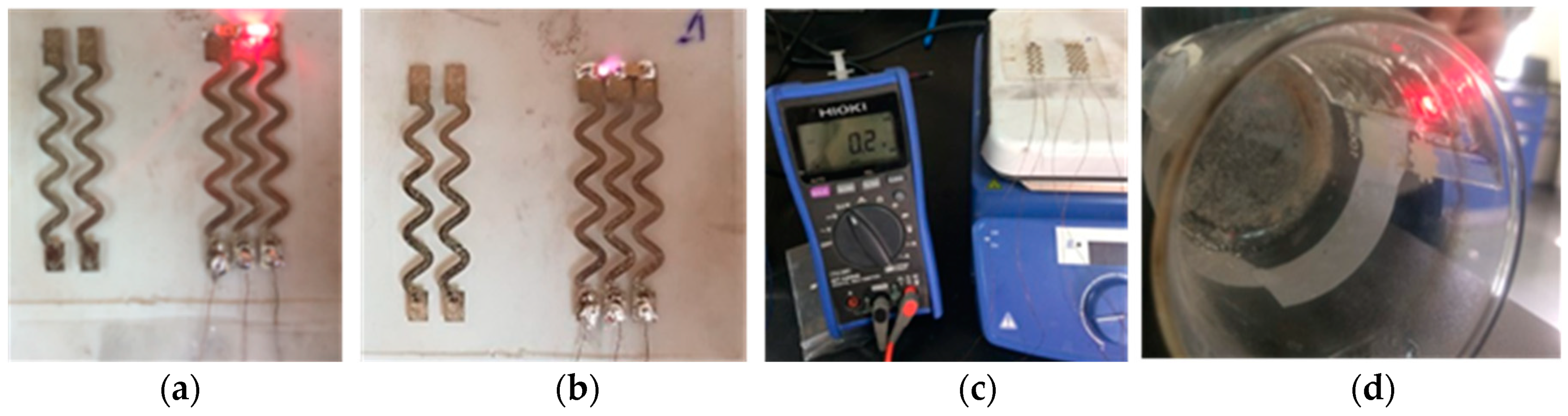
2.1.4. Circuit Testing
2.2. Methodology
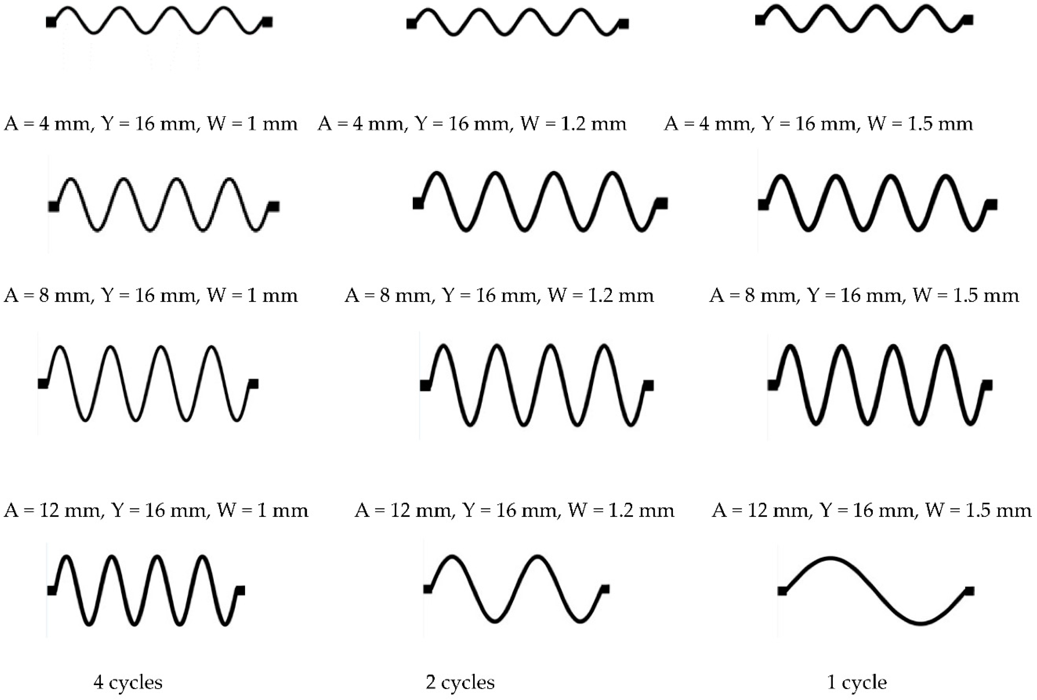
2.2.1. Design of Printed Patterns
2.2.2. Circuit Printing
2.2.3. Stretchable Sensor Development
3. Results and Discussion
3.1. Stretchable Circuit Characterization
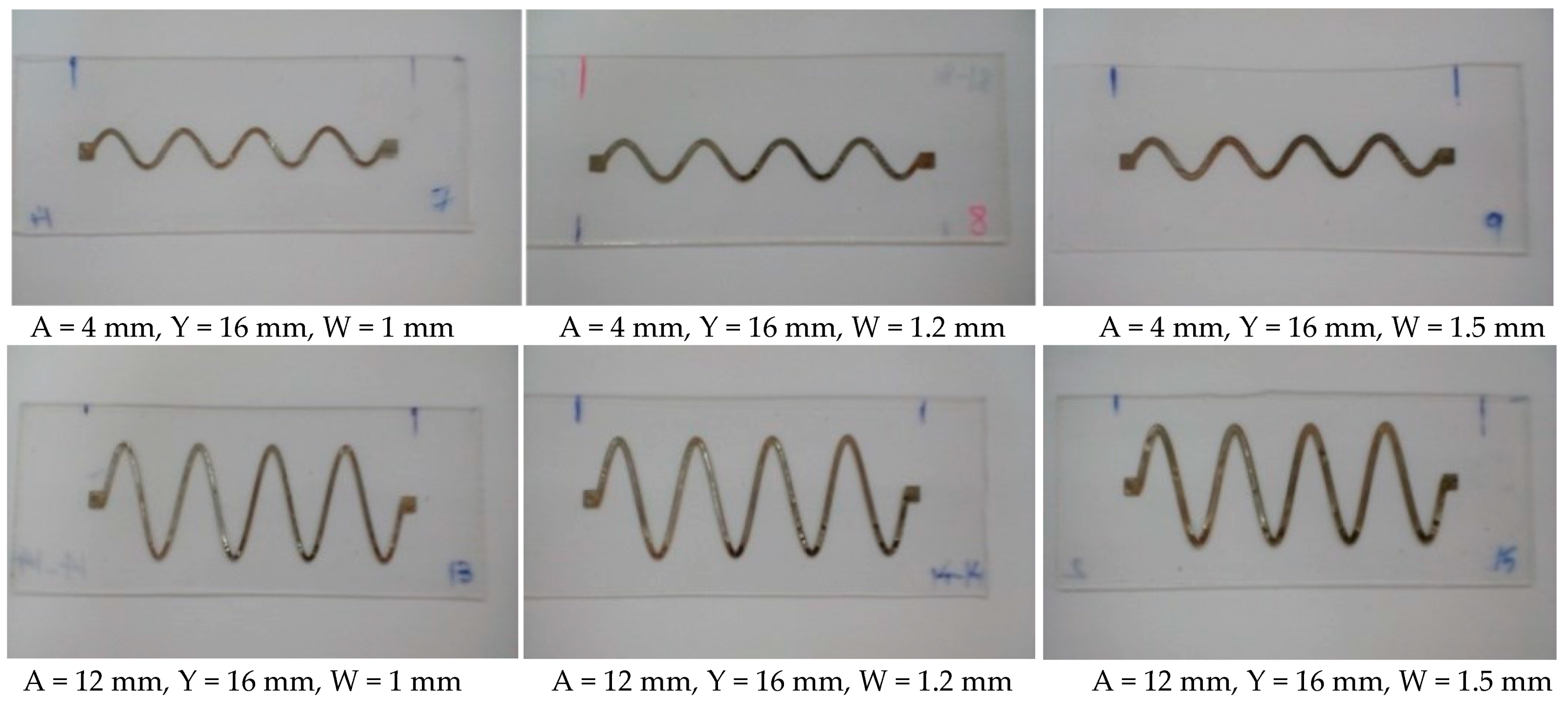
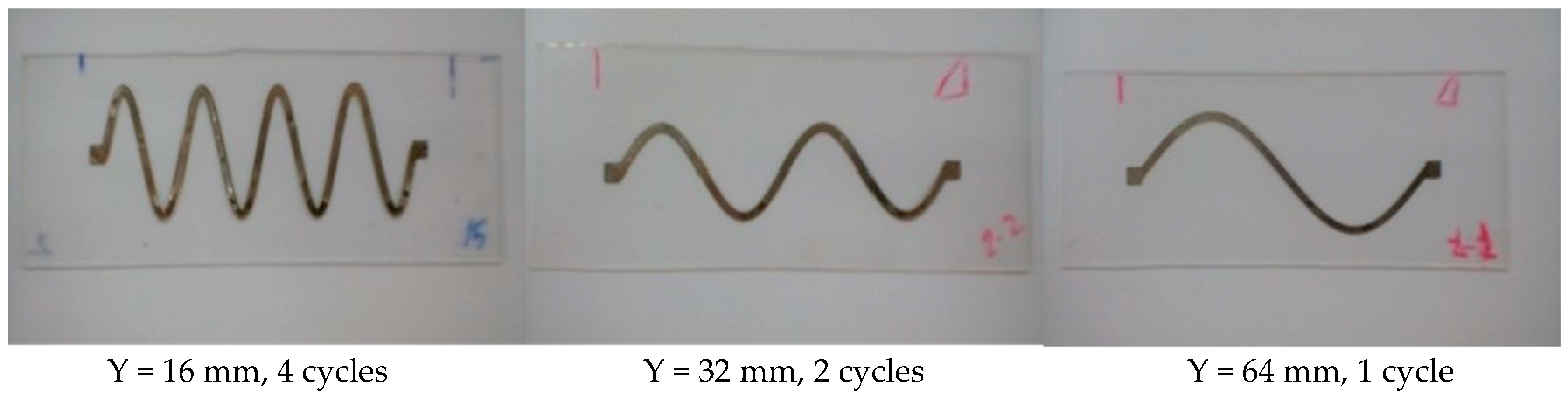
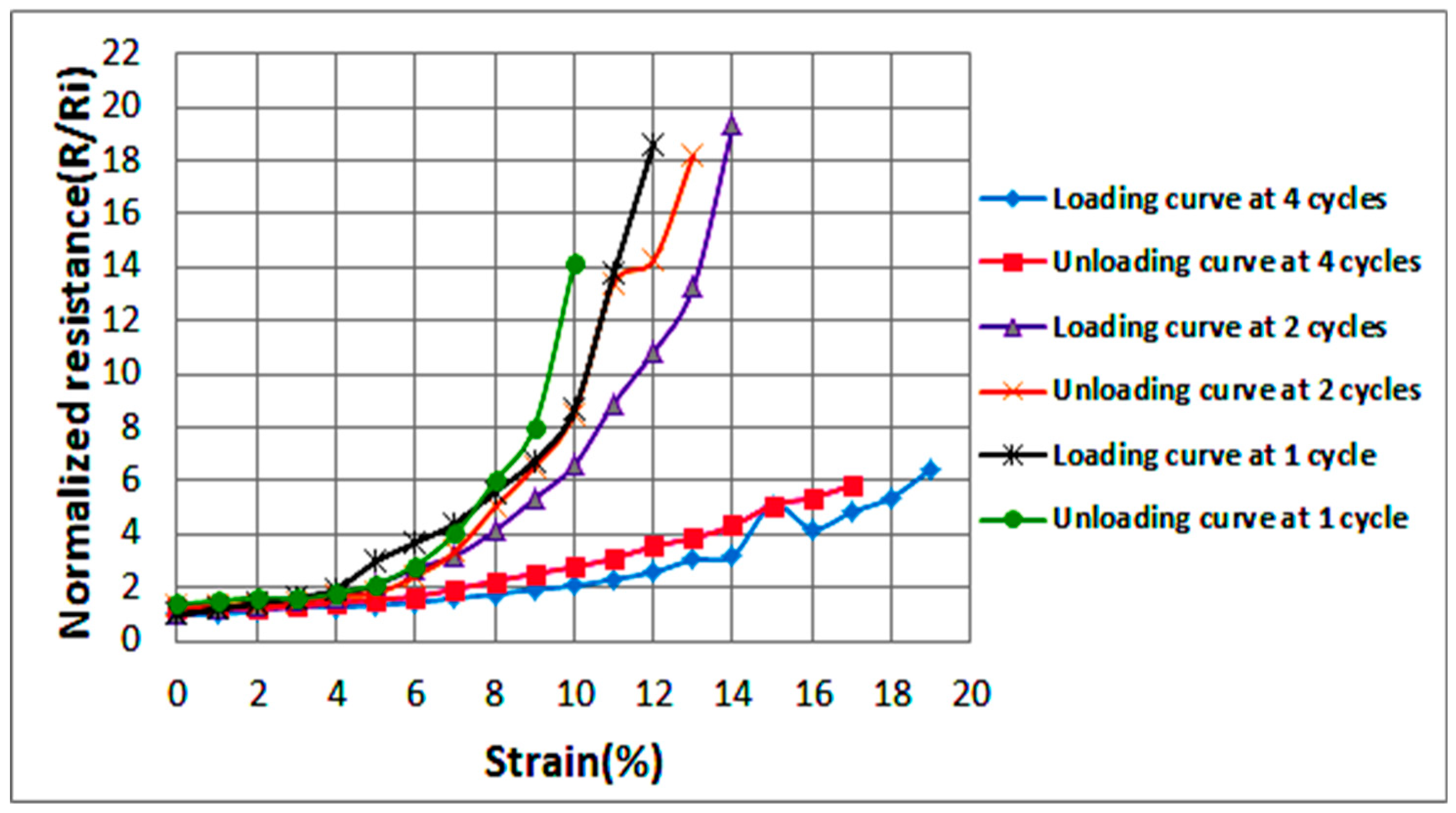
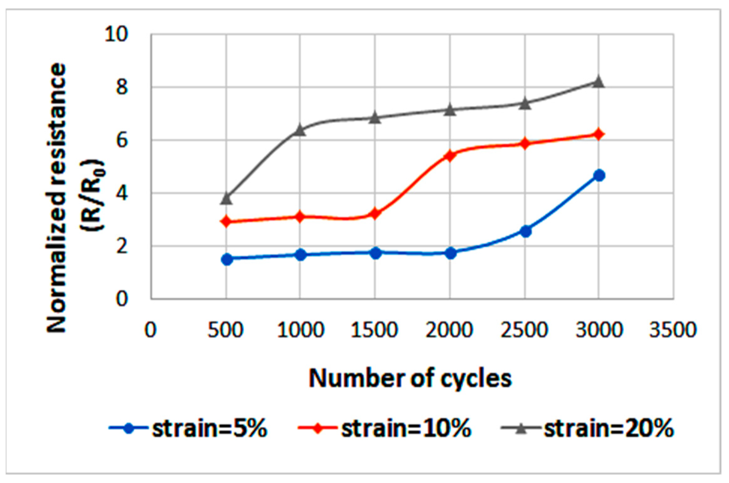
3.1.1. Effect of Conductive Line Geometry on Circuit Performance
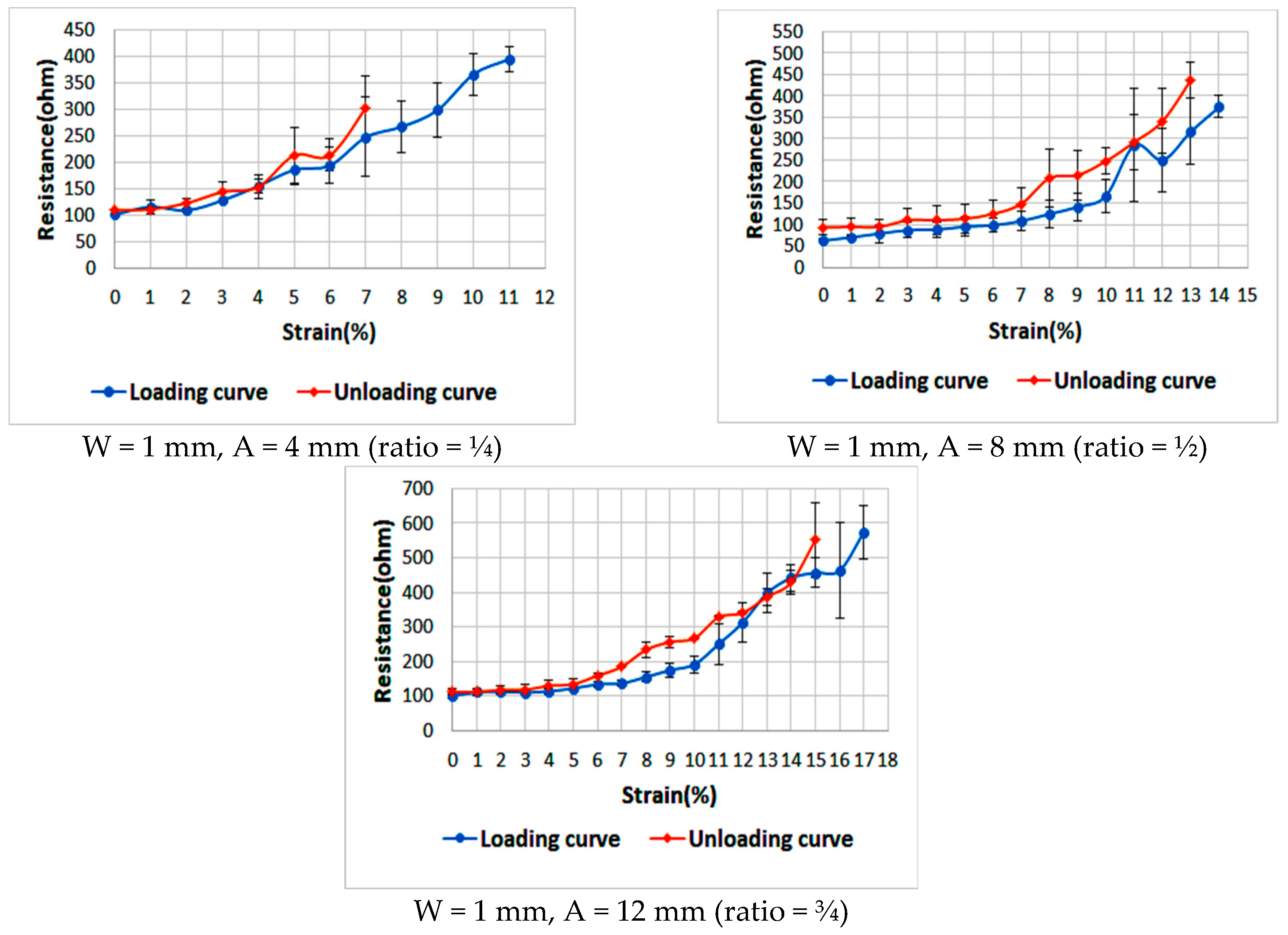
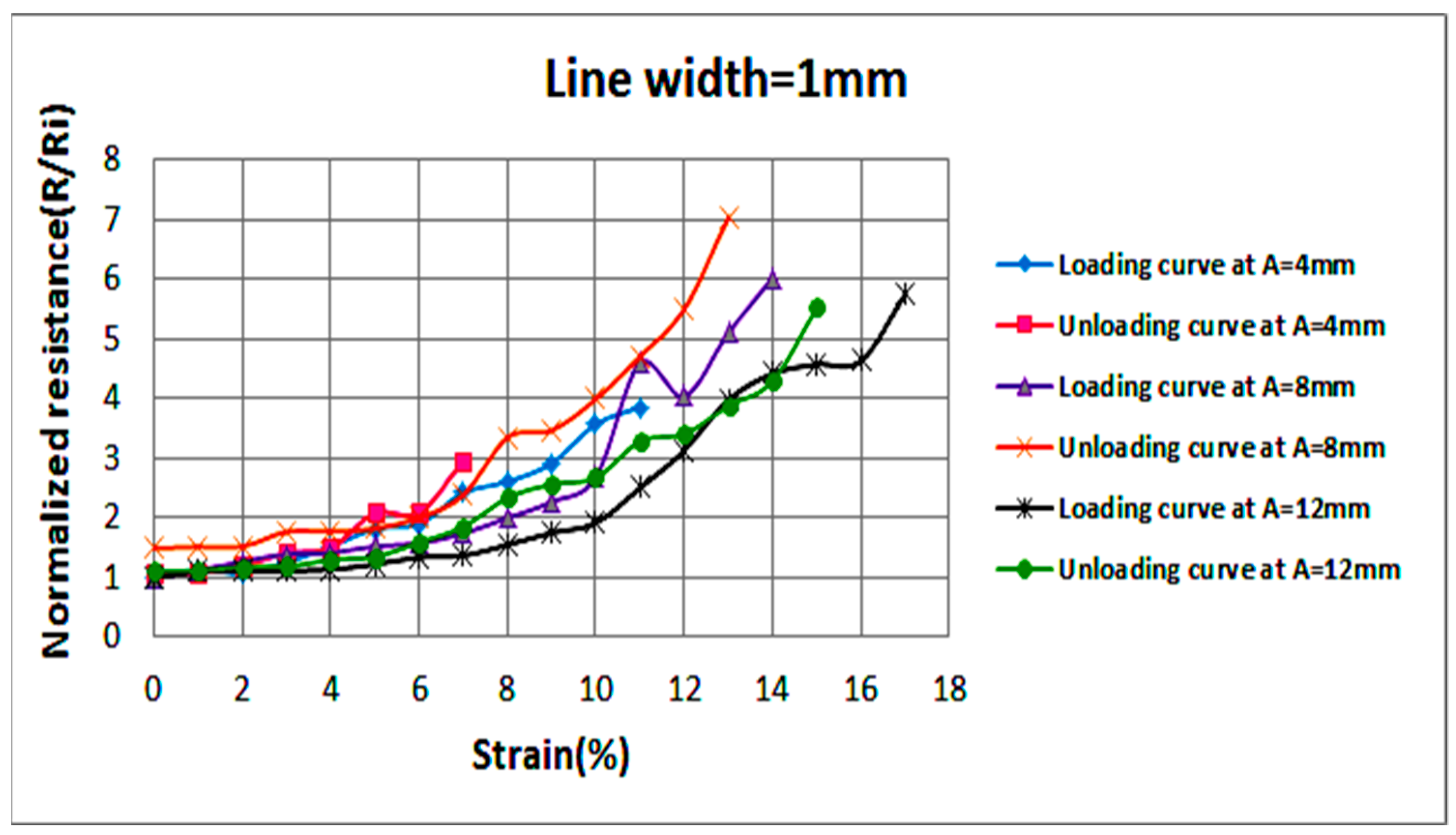
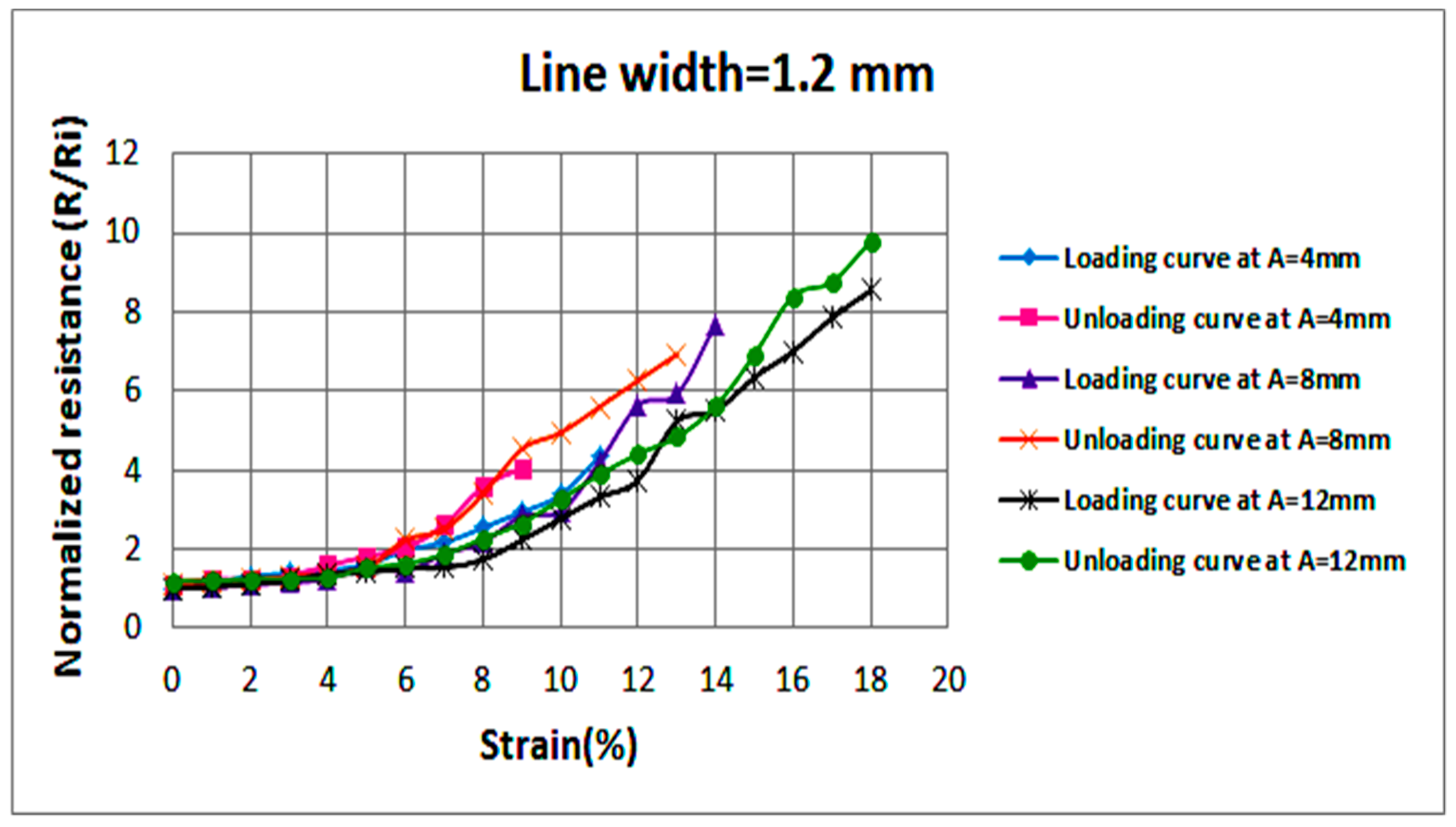
Sinusoidal Patterns
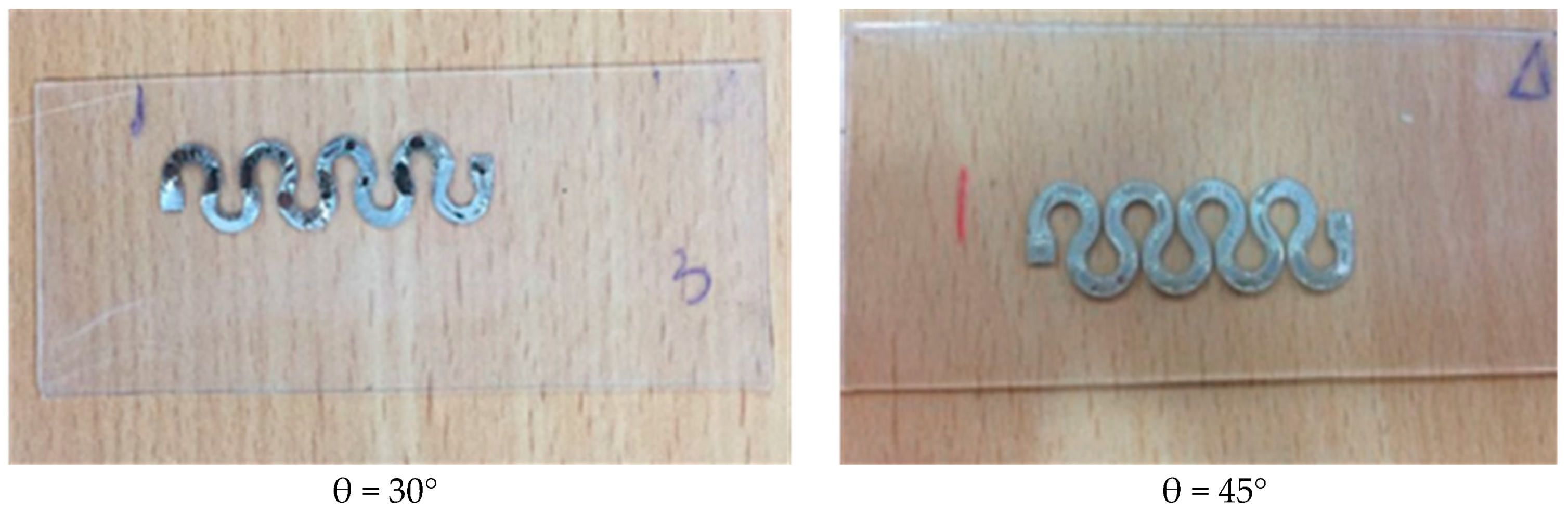
Horseshoe Patterns
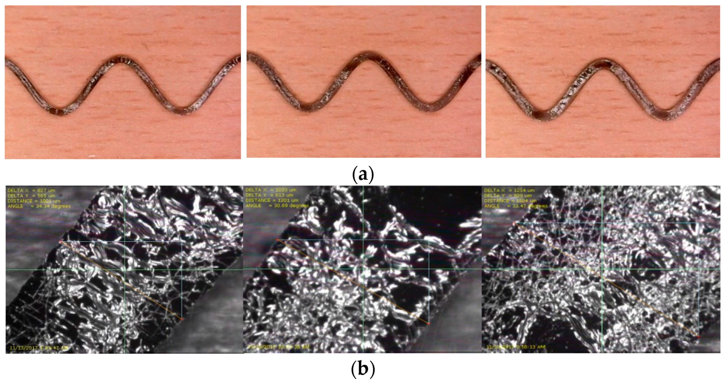
3.1.2. Evaluation of Printed Circuits
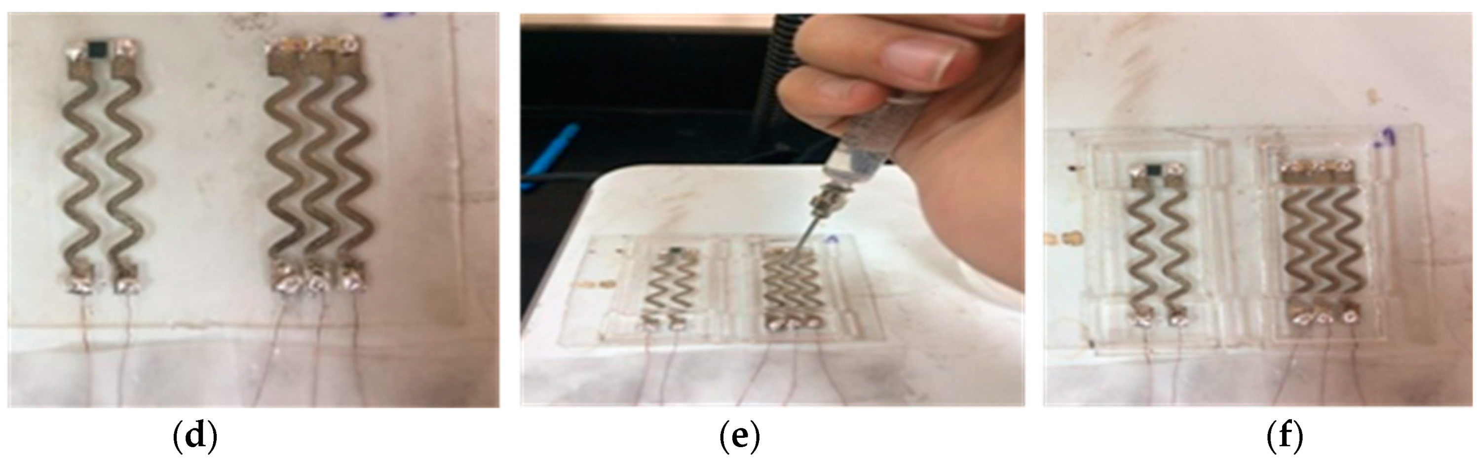
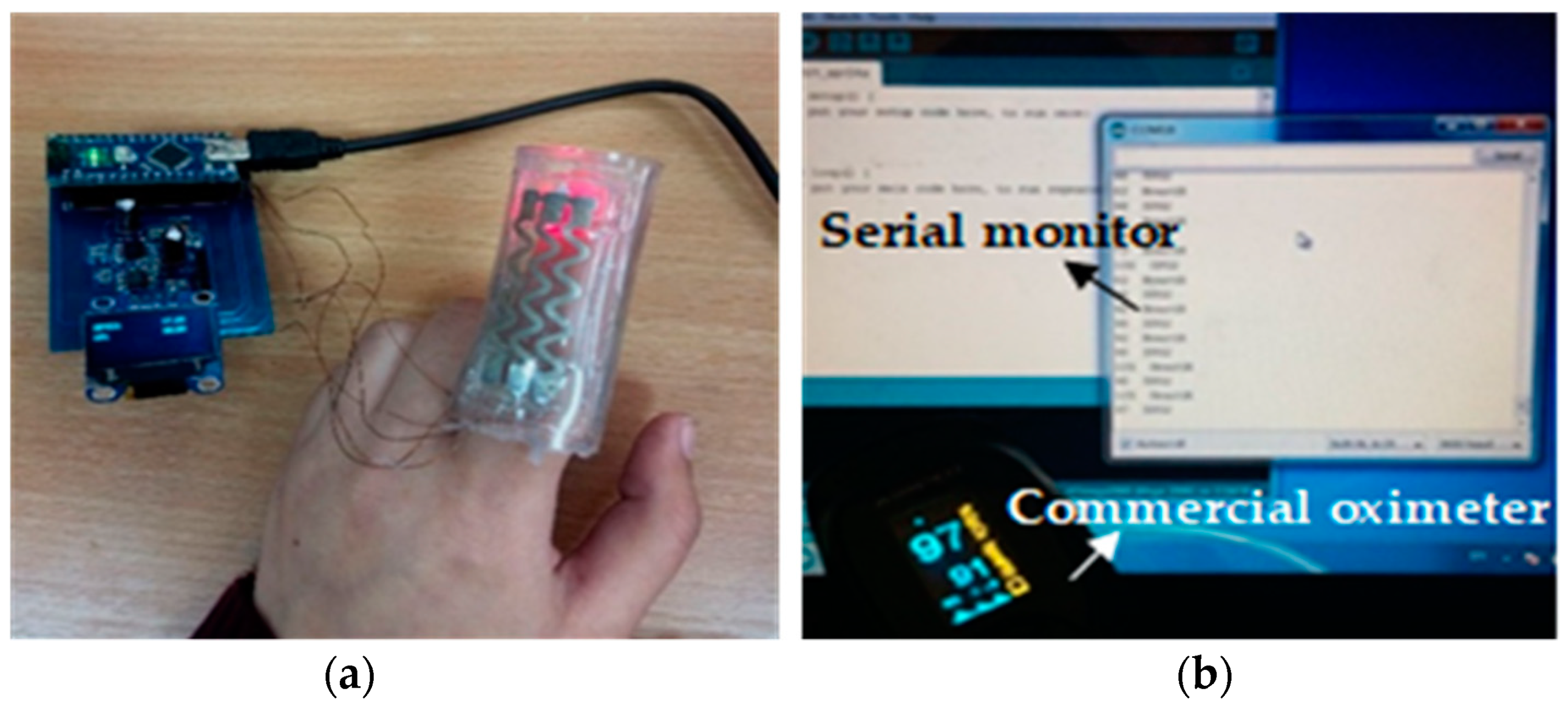
3.2. Wearable Sensor Application
3.2.1. Sensor Assembly
3.2.2. External Conditioning Circuit
4. Conclusions
Supplementary Materials
Author Contributions
Funding
Acknowledgments
Conflicts of Interest
Appendix A


Appendix B
References
- Chang, J.S.; Facchetti, A.F.; Reuss, R. A Circuits and Systems Perspective of Organic/Printed Electronics: Review, Challenges, and Contemporary and Emerging Design Approaches. IEEE J. Emerg. Sel. Top. Circuits Syst. 2017, 7, 7–26. [Google Scholar] [CrossRef]
- Tan, H.W.; Tran, T.; Chua, C.K. A review of printed passive electronic components through fully additive manufacturing methods. Virtual Phys. Prototyp. 2016, 11, 271–288. [Google Scholar] [CrossRef]
- Kessler, F.B.; Kessler, F.B.; Khan, S.; Lorenzelli, L.; Dahiya, R.; Member, S. Technologies for Printing Sensors and Electronics Over Large Flexible Substrates: A Review. IEEE Sens. J. 2015, 15, 3164–3185. [Google Scholar] [CrossRef]
- Mashayekhi, M.; Winchester, L.; Evans, L.; Pease, T.; Laurila, M.M.; Mantysalo, M.; Ogier, S.; Teres, L.; Carrabina, J. Evaluation of Aerosol, Superfine Inkjet, and Photolithography Printing Techniques for Metallization of Application Specific Printed Electronic Circuits. IEEE Trans. Electron Devices 2016, 63, 1246–1253. [Google Scholar] [CrossRef]
- Shinde, S.A.; Jadhav, P.S. A Survey on Printing Technologies. Int. J. Sci. Res. Eng. Technol. 2015, 4, 1165–1170. [Google Scholar]
- Sevilla, G.A.T.; Hussain, M.M. Printed Organic and Inorganic Electronics: Devices to Systems. IEEE J. Emerg. Sel. Top. Circuits Syst. 2017, 7, 147–160. [Google Scholar] [CrossRef]
- Wong, W.; Salleo, A. Flexible Electronics: Materials and Applications Electronic Materials: Science and Technology; Springer: New York, NY, USA, 2009; ISBN 9780387743622. [Google Scholar]
- Castrej, J.R. Future, Opportunities and Challenges of Inkjet Technologies. At. Sprays 2013, 23, 1–13. [Google Scholar]
- Al-Halhouli, A.; Qitouqa, H.; Alashqar, A.; Abu-Khalaf, J. Inkjet printing for the fabrication of flexible/stretchable wearable electronic devices and sensors. Sens. Rev. 2018, 38, 438–452. [Google Scholar] [CrossRef]
- Singh, B.M.; Haverinen, H.M.; Dhagat, P.; Jabbour, G.E. Inkjet Printing—Process and Its Applications. Adv. Mater. 2010, 22, 673–685. [Google Scholar] [CrossRef] [PubMed]
- Haghdoost, F.; Mottaghitalab, V.; Haghi, A.K. Comfortable textile-based electrode for wearable electrocardiogram. Sens. Rev. 2015, 35, 20–29. [Google Scholar] [CrossRef]
- El-Molla, S.; Albrecht, A.; Cagatay, E.; Mittendorfer, P.; Cheng, G.; Lugli, P.; Salmerón, J.F.; Rivadeneyra, A. Integration of a Thin Film PDMS-Based Capacitive Sensor for Tactile Sensing in an Electronic Skin. J. Sens. 2016, 2016. [Google Scholar] [CrossRef]
- Hutchings, I.M.; Martin, G.D. Inkjet Technology for Digital Fabrication; John Wiley & Sons, Ltd.: New York, NY, USA, 2012; ISBN 9781118452943. [Google Scholar]
- Suganuma, K. Printing Technology. In Introduction to Printed ELectronics; Springer: New York, NY, USA, 2014; Volume 74, pp. 23–48. ISBN 978-1-4614-9624-3. [Google Scholar]
- Shafqat, S.; Hoefnagels, J.P.M.; Savov, A.; Joshi, S.; Dekker, R.; Geers, M.G.D. Ultra-stretchable interconnects for high-density stretchable electronics. Micromachines 2017, 8, 277. [Google Scholar] [CrossRef]
- Vaithilingam, J.; Saleh, E.; Tuck, C.; Wildman, R.; Ashcroft, I.; Hague, R.; Dickens, P. 3D-inkjet Printing of Flexible and Stretchable Electronics. In Proceedings of the 26th Solid Freeform Fabrication Symposium, Austin, TX, USA, 10–12 August 2015; pp. 1513–1526. [Google Scholar]
- Liimatta, T.; Halonen, E.; Sillanpaa, H.; Niittynen, J.; Mantysalo, M. Inkjet printing in manufacturing of stretchable interconnects. In Proceedings of the IEEE 64th Electronic Components and Technology Conference, Orlando, FL, USA, 27–30 May 2014; pp. 151–156. [Google Scholar]
- Wu, J.; Roberts, R.C.; Tien, N.C.; Li, D. Inkjet printed silver patterning on PDMS to fabricate microelectrodes for microfluidic sensing. In Proceedings of the IEEE Sensors, Valencia, Spain, 2–5 November 2014. [Google Scholar]
- Sun, J.; Jiang, J.; Bao, B.; Wang, S.; He, M.; Zhang, X.; Song, Y. Fabrication of bendable circuits on a polydimethylsiloxane (PDMS) surface by inkjet printing semi-wrapped structures. Materials 2016, 9, 253. [Google Scholar] [CrossRef] [PubMed]
- Dang, W.; Vinciguerra, V.; Lorenzelli, L.; Dahiya, R. Printable stretchable interconnects. Flex. Print. Electron. 2017, 2, 013003. [Google Scholar] [CrossRef] [Green Version]
- Hocheng, H.; Chen, C.M. Design, fabrication and failure analysis of stretchable electrical routings. Sensors 2014, 14, 11855–11877. [Google Scholar] [CrossRef] [PubMed]
- Van Den Brand, J.; De Kok, M.; Sridhar, A.; Cauwe, M.; Verplancke, R.; Bossuyt, F.; De Baets, J.; Vanfleteren, J. Flexible and stretchable electronics for wearable healthcare. In Proceedings of the 44th European Solid-State Device Research Conference, Venice, Italy, 22–26 September 2014; pp. 206–209. [Google Scholar]
- Servati, A.; Zou, L.; Wang, Z.; Ko, F.; Servati, P. Novel Flexible Wearable Sensor Materials and Signal Processing for Vital Sign and Human Activity Monitoring. Sensors 2017, 17, 1622. [Google Scholar] [CrossRef] [PubMed]
- Xiao, J.; Carlson, A.; Liu, Z.J.; Huang, Y.; Jiang, H.; Rogers, J.A. Stretchable and compressible thin films of stiff materials on compliant wavy substrates. Appl. Phys. Lett. 2008, 93, 013309. [Google Scholar] [CrossRef]
- Lacour, S.P.; Jones, J.; Suo, Z.; Wagner, S. Design and Performance of Thin Metal Film Interconnects for Skin-Like Electronic Circuits. IEEE Electron Device Lett. 2004, 25, 179–181. [Google Scholar] [CrossRef] [Green Version]
- Dahne, L.; Radtchenko, I.; Antipov, A.; Gao, C.; Ser, S.S.; Gray, B.D.S.; Tien, J.; Chen, C.S. High-Conductivity Elastomeric Electronics. Adv. Mater. 2004, 16, 393–397. [Google Scholar] [CrossRef]
- Brosteaux, D.; Axisa, F.; Gonzalez, M.; Vanfleteren, J. Design and fabrication of elastic interconnections for stretchable electronic circuits. IEEE Electron Device Lett. 2007, 28, 552–554. [Google Scholar] [CrossRef]
- Nagels, S.; Deferme, W. Fabrication approaches to interconnect based devices for stretchable electronics: A review. Materials 2018, 11, 375. [Google Scholar] [CrossRef] [PubMed]
- Song, J. Mechanics of stretchable electronics. Curr. Opin. Solid State Mater. Sci. 2015, 19, 160–170. [Google Scholar] [CrossRef]
- Lu, N.; Yang, S. Mechanics for stretchable sensors. Curr. Opin. Solid State Mater. Sci. 2015, 19, 149–159. [Google Scholar] [CrossRef]
- Gao, M.; Li, L.; Song, Y. Inkjet printing wearable electronic devices. J. Mater. Chem. C 2017, 5, 2971–2993. [Google Scholar] [CrossRef]
- Joshi, S.; Savov, A.; Dekker, R. Substrate Transfer Technology for Stretchable Electronics. Procedia Eng. 2016, 168, 1555–1558. [Google Scholar] [CrossRef]
- Cho, K.; Koh, J.; Kim, S.; Chu, W.; Hong, Y.; Ahn, S. Review of manufacturing processes for soft biomimetic robots Review of Manufacturing Processes for Soft Biomimetic Robots. Int. J. Precis. Eng. Manuf. 2009, 10, 171. [Google Scholar] [CrossRef]
- Kim, Y.; Ren, X.; Kim, J.W.; Noh, H. Direct inkjet printing of micro-scale silver electrodes on polydimethylsiloxane (PDMS) microchip. J. Micromech. Microeng. 2014, 24, 115010. [Google Scholar] [CrossRef]
- Wu, J.; Wang, R.; Yu, H.; Li, G.; Xu, K.; Tien, N.C.; Roberts, R.C.; Li, D. Inkjet-printed microelectrodes on PDMS as biosensors for functionalized microfluidic systems. Lab Chip 2015, 15, 690–695. [Google Scholar] [CrossRef] [PubMed]
- Cummins, G.; Desmulliez, M.P.Y. Inkjet printing of conductive materials: A review. Circuit World 2012, 38, 193–213. [Google Scholar] [CrossRef]
- Dickey, M.D.; Chiechi, R.C.; Larsen, R.J.; Weiss, E.A.; Weitz, D.A.; Whitesides, G.M. Eutectic gallium-indium (EGaIn): A liquid metal alloy for the formation of stable structures in microchannels at room temperature. Adv. Funct. Mater. 2008, 18, 1097–1104. [Google Scholar] [CrossRef]
- Hu, A.; Shaikh, K.; Liu, C. Super flexible sensor skin using liquid metal as interconnect. In Proceedings of the IEEE Sensors, Atlanta, GA, USA, 28–31 October 2007; pp. 815–817. [Google Scholar]
- Hu, H.; Liu, C. Characterizations and optimization of electrical contact between nanocomposite elastomer and metal. In Proceedings of the TRANSDUCERS 2009—15th International Conference on Solid-State Sensors, Actuators and Microsystems, Denver, CO, USA, 21–25 June 2009; pp. 1103–1105. [Google Scholar]
- Kim, H.J.; Son, C.; Ziaie, B. A multiaxial stretchable interconnect using liquid-alloy-filled elastomeric microchannels. Appl. Phys. Lett. 2008, 92, 011904. [Google Scholar] [CrossRef] [Green Version]
- Kim, H.J.; Zhang, M.; Ziaie, B. A biaxially stretchable interconnect with liquid alloy joints on flexible substrate. In Proceedings of the TRANSDUCERS and EUROSENSORS ’07—4th International Conference on Solid-State Sensors, Actuators and Microsystems, Lyon, France, 10–14 June 2007; pp. 1597–1600. [Google Scholar]
- Abu-Khalaf, J.M.; Mascaro, S.A. Optimization of Stretchable Fingernail Sensor Design for Fingertip Force Direction Estimation. In Proceedings of the IEEE Sensors Applications Symposium (SAS), Seoul, South Korea, 12–14 March 2018. [Google Scholar]
- Mascaro, D.J.; Mascaro, S.A. Stretchable Fingernail Sensors for Measurement of Fingertip Force. In Proceedings of the World Haptics 2009—Third Joint EuroHaptics conference and Symposium on Haptic Interfaces for Virtual Environment and Teleoperator Systems, Salt Lake City, UT, USA, 18–20 March 2009; pp. 625–626. [Google Scholar]
- Schausberger, S.E.; Kaltseis, R.; Drack, M.; Cakmak, U.D.; Major, Z.; Bauer, S. Cost-Efficient Open Source Desktop Size Radial Stretching System With Force Sensor. IEEE Access 2015, 3, 556–561. [Google Scholar] [CrossRef]
- Mamidanna, A.; Lefky, C.; Hildreth, O. Drop-on-demand printed microfluidics device with sensing electrodes using silver and PDMS reactive inks. Microfluid. Nanofluidics 2017, 21, 172. [Google Scholar] [CrossRef]
- Mendelson, Y. Pulse oximetry: Theory and applications for noninvasive monitoring. Clin. Chem. 1992, 38, 1601–1607. [Google Scholar] [PubMed]


| Drop Spacing (µm) | Resistance (ohm) | Line Width (µm) |
|---|---|---|
| 5 | 0.4 | 2591.2 |
| 10 | 1.5 | 1862.6 |
| 15 | 2.6 | 1805.1 |
| 20 | 8 | 1620.2 |
| 25 | 15 | 1612 |
| 30 | 24.9 | 1611.9 |
| Printing Parameters | Values |
|---|---|
| Nozzle/cartridge temperature | 32 °C |
| Platen temperature | 26 °C (room temperature) |
| Firing voltage | 23 volts |
| Speed | 8 m/s |
| Sintering temperature and time | 150 °C for 1 h |
| Amplitude (mm) | Width (mm) | |||||
|---|---|---|---|---|---|---|
| 1 | 1.2 | 1.5 | ||||
| Sample 1 | Sample 2 | Sample 1 | Sample 2 | Sample 1 | Sample 2 | |
| 4 (Ratio = ¼) | Ri = 102.1 Ω Rf = 372.1 Ω S% = 11% | Ri = 102.8 Ω Rf = 417.6 Ω S% = 11% | Ri = 72.1 Ω Rf = 269.2 Ω S% = 12% | Ri = 74.3 Ω Rf = 446.2 Ω S% = 11% | Ri = 59 Ω Rf = 0.7 KΩ S% = 14% | Ri = 62.3 Ω Rf = 0.6 KΩ S% = 16% |
| 8 (Ratio = ½) | Ri = 65 Ω Rf = 0.4 KΩ S% = 14% | Ri = 59.2 Ω Rf = 349.9 Ω S% = 15% | Ri = 55.5 Ω Rf = 389.3 Ω S% = 15% | Ri = 48.6 Ω Rf = 432.6 Ω S% = 14% | Ri = 53.6 Ω Rf = 493.3 Ω S% = 18% | Ri = 47.2 Ω Rf = 426.4 Ω S% = 19% |
| 12 (Ratio = ¾) | Ri = 105.5 Ω Rf = 0.8 KΩ S% = 17% | Ri = 94.2 Ω Rf = 497 Ω S% = 18% | Ri = 72.6 Ω Rf = 0.65 KΩ S% = 18% | Ri = 71.3 Ω Rf = 0.56 KΩ S% = 18 | Ri = 68 Ω Rf = 461.7 Ω S% = 21% | Ri = 75.6 Ω Rf = 513.6 Ω S% = 19% |
| Theta = 30° L = 45 mm | Theta = 45° L = 37.8 mm | ||
|---|---|---|---|
| Sample 1 | Sample 2 | Sample 1 | Sample 2 |
| Ri = 15.2 Ω Rf = 700 Ω S% = 24% | Ri = 17.2 Ω Rf = 790 Ω S% = 21% | Ri = 13.6 Ω Rf = 622.8 Ω S% = 25% | Ri = 14.7 Ω Rf = 770 Ω S% = 24% |
| Subject | Gender | Heart Rate (HR) | Oxygen Saturation (SPO2) | ||
|---|---|---|---|---|---|
| Observed | Actual | Observed | Actual | ||
| 1 | Female | 91 | 94 | 97 | 97 |
| 2 | Female | 78 | 80 | 98 | 98 |
| 3 | Female | 61 | 66 | 99 | 99 |
| 4 | Female | 89 | 81 | 96 | 97 |
| 5 | Female | 75 | 79 | 98 | 96 |
| 6 | Female | 72 | 75 | 98 | 98 |
| 7 | Female | 82 | 78 | 99 | 98 |
| 8 | Female | 82 | 81 | 99 | 97 |
| 9 | Female | 81 | 77 | 95 | 98 |
| 10 | Female | 86 | 84 | 98 | 98 |
| 11 | Male | 78 | 79 | 97 | 98 |
| 12 | Male | 74 | 71 | 96 | 96 |
| 13 | Male | 84 | 80 | 98 | 98 |
| 14 | Male | 80 | 81 | 97 | 98 |
| 15 | Male | 89 | 90 | 98 | 98 |
| 16 | Male | 85 | 91 | 96 | 96 |
| 17 | Male | 75 | 70 | 98 | 98 |
| 18 | Male | 79 | 72 | 95 | 97 |
| 19 | Male | 77 | 80 | 99 | 98 |
| 20 | Male | 87 | 80 | 97 | 95 |
© 2018 by the authors. Licensee MDPI, Basel, Switzerland. This article is an open access article distributed under the terms and conditions of the Creative Commons Attribution (CC BY) license (http://creativecommons.org/licenses/by/4.0/).
Share and Cite
Abu-Khalaf, J.; Saraireh, R.; Eisa, S.; Al-Halhouli, A. Experimental Characterization of Inkjet-Printed Stretchable Circuits for Wearable Sensor Applications. Sensors 2018, 18, 3476. https://doi.org/10.3390/s18103476
Abu-Khalaf J, Saraireh R, Eisa S, Al-Halhouli A. Experimental Characterization of Inkjet-Printed Stretchable Circuits for Wearable Sensor Applications. Sensors. 2018; 18(10):3476. https://doi.org/10.3390/s18103476
Chicago/Turabian StyleAbu-Khalaf, Jumana, Razan Saraireh, Saleh Eisa, and Ala’aldeen Al-Halhouli. 2018. "Experimental Characterization of Inkjet-Printed Stretchable Circuits for Wearable Sensor Applications" Sensors 18, no. 10: 3476. https://doi.org/10.3390/s18103476