Frequency Response of Graphene Electrolyte-Gated Field-Effect Transistors


Massachusetts Institute of Technology, Department of Electrical Engineering and Computer Science, 77 Massachusetts Avenue, Cambridge, MA 02139, USA
*
Author to whom correspondence should be addressed.
Sensors 2018, 18(2), 494; https://doi.org/10.3390/s18020494
Submission received: 16 January 2018
/
Revised: 31 January 2018
/
Accepted: 1 February 2018
/
Published: 7 February 2018
(This article belongs to the Special Issue Thin-Film Transistors for Biomedical and Chemical Sensing)
Abstract
:This work develops the first frequency-dependent small-signal model for graphene electrolyte-gated field-effect transistors (EGFETs). Graphene EGFETs are microfabricated to measure intrinsic voltage gain, frequency response, and to develop a frequency-dependent small-signal model. The transfer function of the graphene EGFET small-signal model is found to contain a unique pole due to a resistive element, which stems from electrolyte gating. Intrinsic voltage gain, cutoff frequency, and transition frequency for the microfabricated graphene EGFETs are approximately 3.1 V/V, 1.9 kHz, and 6.9 kHz, respectively. This work marks a critical step in the development of high-speed chemical and biological sensors using graphene EGFETs.
1. Introduction
Graphene consists of an atomically thin layer of sp2-bonded carbon atom arranged in a hexagonal lattice [1,2,3,4]. Although graphene lacks a bandgap and is ill suited for traditional digital logic circuits, graphene exhibits a number of promising electrical, optical, mechanical, and chemical properties making it well suited for a variety of chemical and biological sensing applications. Key properties include high carrier mobilities [5], low optical absorption [6,7], mechanical strength and flexibility [6,7,8,9,10], as well as chemical stability [11,12,13,14]. Because graphene exhibits excellent chemical stability and does not form a native oxide like its silicon metal-oxide-semiconductor field-effect transistor (Si-MOSFET) counterparts, graphene electrolyte-gated field-effect transistors (EGFETs) can take full advantage of the ultrahigh gate capacitance resulting from the electric double layer phenomenon [15]. Excellent chemical stability also enables a direct interface with many chemical and biological environments [11,13,14,16]. This ultra-high gate capacitance, which is in the order of μF/cm2, provides graphene EGFETs with excellent transconductance performance [17,18]. It also raises the concern of impaired frequency response due to high parasitic gate-source and gate-drain capacitances. This is especially concerning in the case of graphene EGFETs because transconductance performance is greatly enhanced by recessing device passivation such that portions of the source and drain contacts are exposed [19].
A number of models have been developed describing the DC behavior of graphene FETs, including two models which accurately describe DC characteristics of graphene EGFETs [20,21,22,23,24,25]. Little work, however, has been reported regarding the AC capabilities of graphene EGFETs. Accurate frequency response models are critical in the development of graphene EGFETs for applications such as electrophysiology sensors. Previous studies have shown graphene EGFETs capable of providing low-noise signal transduction for neuronal action potentials [16,26]. These studies, however, employ graphene EGFETs merely for source-drain current modulation (i.e., as tunable resistors) and therefore result in greatly attenuated action potential signals.
The aim of this paper is two-fold: to advance graphene EGFET sensing technology for applications such as electrophysiology by demonstrating the ability of graphene EGFETs to operate as functional amplifiers, and to develop the corresponding small-signal frequency-dependent model necessary to understand the amplification characteristics. Development of high-speed graphene EGFETs may find use as chemical sensors in applications such as high-throughput microfluidics [27]. Characterization of frequency response for the first time also enables entirely new sensing technologies, such as electronic tongues, where changes in the frequency response (i.e., spectral content) may be analyzed to sense changes in solution composition. This is closely related to spectroscopic and time constant techniques employed in electronic nose technologies [28,29,30]. Lastly, frequency response characterization is critical in avoiding signal aliasing when interfacing graphene EGFET sensors with analog-to-digital (ADC) converters in the development of practical sensor readout systems [31].
2. Graphene EGFET Background
2.1. Graphene-Electrolyte Interface Capacitance
Immersion of an electrode in an electrolyte results in the accumulation of ions at the electrode/electrolyte interface due to differences in electrochemical potential. This phenomenon is termed the electric double layer. The amount of charge stored in the electric double layer may be controlled—much like a capacitor—by changing the electric potential of the electrode with respect to the electrolyte potential [32]. In the case of graphene, the capacitance of the electric double layer is large enough that accurately modeling the graphene-electrolyte interface capacitance requires inclusion of the graphene quantum capacitance [15]. Quantum capacitance is proportional to the density of states and places an upper bound on the capacitance achievable in two-dimensional materials such as graphene. The graphene quantum capacitance is critical to understanding the effects of parasitic capacitances on graphene EGFET frequency response. Equations (1) and (2) describe the graphene quantum capacitance [18].
Here is the reduce Planck constant, is the Fermi velocity, is the carrier concentration induced by the gate voltage, is the effective charged impurity concentration, and is the electric potential of the graphene channel.
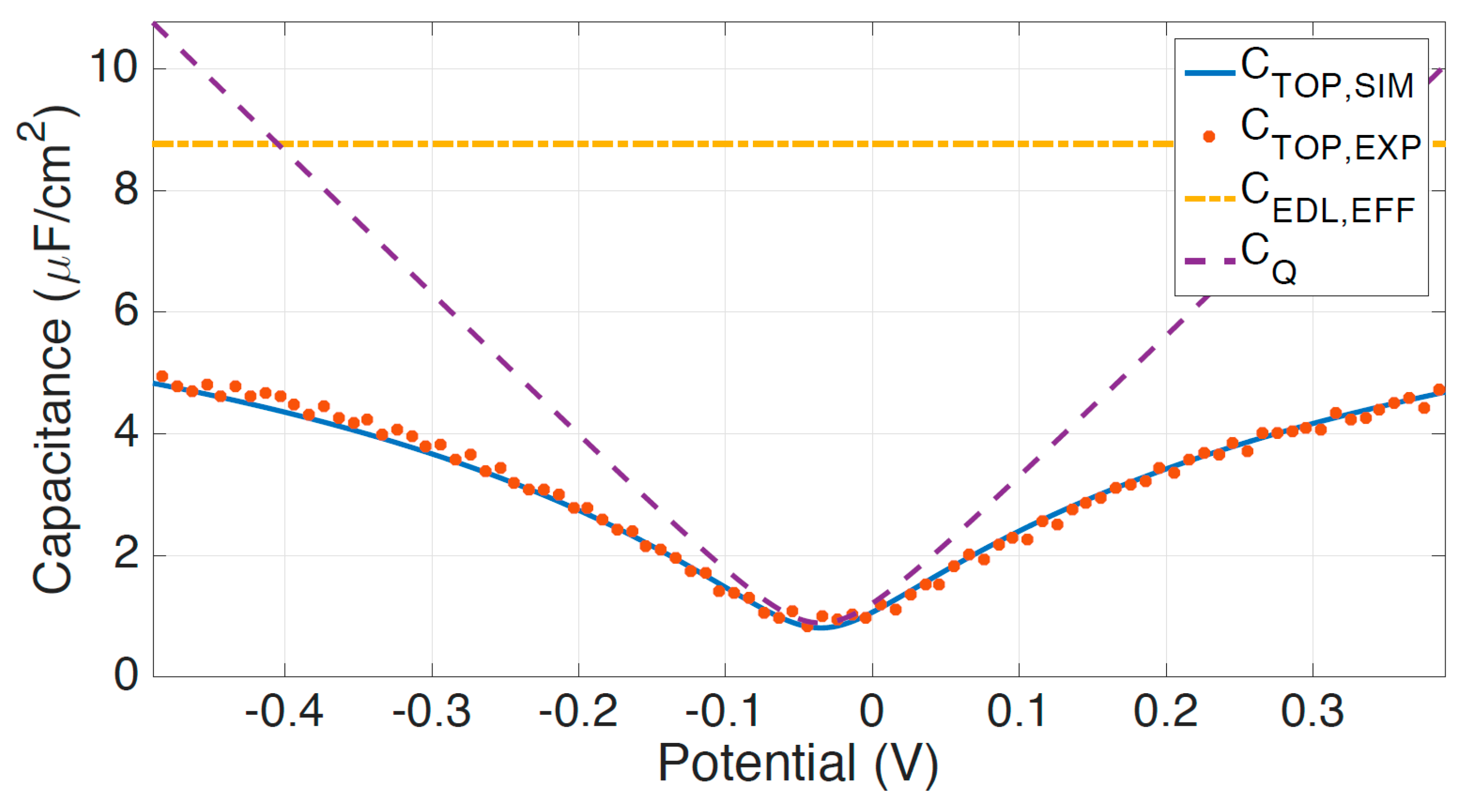
Graphene-electrolyte interface capacitances have been experimentally examined in numerous works [17,19,33,34]. The graphene/electrolyte interface capacitance may be modeled using a parallel plate capacitor in series with the graphene quantum capacitance. As a hydrophobic material, graphene repels aqueous electrolytes resulting in an angstrom-scale gap between the electrolyte and graphene surface. This forms a parallel plate capacitor, which reduces the complex voltage-dependence capacitance typical of electric double layers. Ultimately, graphene-electrolyte interface capacitances typically range from approximately 1–5 μF/cm2 as measured by electrochemical impedance spectroscopy (EIS), and shown in Figure 1. The mean value of the graphene-electrolyte interface capacitance is 3 μF/cm2, which is useful for approximations.
2.2. Graphene EGFET DC Current-Voltage Model
Graphene EGFETs are comprised of two conductive contacts, typically metals, connected by a graphene channel region. The bulk of the metal leads are passivated to reduce leakage current through the electrolyte due to applied gate voltage. The graphene channel region is gated directly through the electrolyte using a reference or pseudo-reference electrode. Figure 2 depicts the typical layout for a graphene EGFET and experimental setup.
The current at any given position in the graphene channel is determined by the product of carrier concentration and the carrier drift velocity, which is scaled appropriately by the elementary charge and channel width. This principle, in conjunction with current continuity, enables calculation of the graphene EGFET current and the corresponding channel potential profile. The channel current is given by the following equation [19,20,35]:
where is the channel width and is the channel length, is the carrier mobility, and V is the channel potential which is a function of position, is the minimum carrier concentration [36,37], is the top-gate capacitance, is the applied top gate voltage, is the saturation velocity, is the contact resistance, and Vo represents the gate voltage at the Dirac point. This particular model assumes carrier mobilities are equal for holes and electrons and independent of the carrier concentration. Contact resistances are assumed to be symmetric. It is also important to note that chemical and biological sensors employing graphene EGFETs are typically biased at low voltages to avoid undesirable reduction-oxidation reactions of chemical species in the electrolyte. Because of this, carrier drift velocity is typically well below the saturation velocity. Saturation velocity is included nonetheless for completeness.
2.3. Graphene EGFET Small-Signal Model
The graphene EGFETs under study are three terminal devices possessing source, drain, and gate terminals. All voltages and currents are referenced with respect to the source terminal making , , and an exhaustive list of the voltages and currents of interest. Small signal intrinsic voltage gain is defined as , where is the transconductance, which is defined as , and is the output impedance defined as . Development of a frequency-dependent graphene EGFET small-signal model requires an accurate model for electrode-electrolyte interfaces. This is accomplished using a simplified Randles circuit as given by Figure 3 [38,39].
represents the charge transfer resistance, is the solution resistance, and is the double layer capacitance. Electrode-electrolyte interfaces occur in three locations: the electrolyte-source interface, the electrolyte-drain interface, and at the reference electrode’s interface with the electrolyte. The simplified Randles circuit is substituted into the small-signal model at each of these locations. Graphene is known to possess a wide electrochemical window in electrolytic environments [11]. This translates into a very high charge transfer resistance , roughly on the order of GΩ. Because of this, can be safely neglected at the gate-source and gate-drain terminals. This leads to the small-signal graphene EGFET model depicted in Figure 4.
Electrochemistry experiments possess two interfaces, only one of which is the focus of study. In this case, the first interface exists between the reference electrode and electrolyte and the second interface occurs between the electrolyte and graphene EGFET. Reference electrodes are specifically designed to provide a stable reference potential and effectively translate changes in applied voltage entirely to the interface under study. This means that the reference electrode effectively translates the entirety of the small signal voltage to the graphene EGFET and electrolyte interface. Because no series voltage drop occurs at the reference electrode, the simplified Randles circuit for the reference electrode may be neglected. Applying this fact in conjunction with the Miller theorem leads to the final small-signal model depicted in Figure 5.
This small-signal model for graphene EGFETs leads to the transfer function given by Equation (4).
It becomes evident that the graphene EGFET small-signal model, unlike a Si-MOSFETs possesses a resistive component in series with the output parasitic capacitance. This unique component stems from the fact that graphene EGFETs are electrolyte-gated. Looking at the transfer function in the limits of low and high frequency operation produces the Equations (5) and (6), respectively.
and are given by Equations (7) and (8). Because gain is a negative value, the absolute value of the gain is used for clarity in showing how the magnitude of parasitic impedances are amplified at the input.
Similarly, equivalent impedances at the output are slightly reduced and given by Equations (9) and (10). This wholly details the development of the graphene EGFET small-signal model from first principles and provides the necessary reference equations describing individual model components.
3. Materials and Methods
3.1. Graphene EGFET Fabrication
Graphene EGFETs were fabricated on a piranha cleaned 4” thermally oxidized silicon wafer. Source and drain Ti/Au (10 nm/150 nm) contacts were patterned using lift-off photolithography. Monolayer graphene was then grown on copper foils using chemical vapor deposition (CVD) and transferred over the entire substrate [40]. The graphene channel regions were defined using MMA/SPR700 bilayer resist stacks and helium and oxygen plasma at 16 sccm and 8 sccm, respectively. Bilayer photoresist stacks were removed using acetone and isopropanol. The entire wafer was passivated with approximately 0.6 μm of SU-8 2000.5 and windows were photo defined to provide electrolyte access to the graphene EGFET channel regions. The SU-8 was hard-baked at 150 °C for five minutes to help remove cracks and pinholes. Figure 6 depicts a graphene EGFET at various stages in the fabrication process. An aqueous electrolyte droplet of 100 mM NaCl was pipetted over the graphene EGFET channel regions and a reference electrode was inserted into the droplet to gate the devices. Aqueous 100 mM NaCl was chosen because of its charge symmetry and similarity to physiological osmolarity.
3.2. Experimental Setup
Two experimental setups were employed for graphene EGFET characterization: one for DC characterization and one for AC characterization. DC characterization was performed to measure the graphene EGFET drain-source current and a function of and . This enables the calculation of transconductance, output impedance as well as intrinsic voltage gain. DC characterization also provides an independent means for measuring intrinsic voltage gain. In that way, DC and AC voltage gains can be compared and verified as consistent. AC characterization was performed by applying a small-signal voltage to a common-source graphene EGFET amplifier and measuring the resulting output voltage as a function of frequency.
The graphene EGFET experimental data is obtained from a device with dimensions W/L = 30 μm/30 μm and recessed passivation such that approximately 10 μm of the drain and source contacts were exposed to electrolyte. The device was measured in 100 mM aqueous NaCl electrolyte. DC measurements employed a platinum wire pseudo reference electrode for convenience. AC measurements require the use of a Ag/AgCl reference electrode. All measurements are taken at room temperature under ambient conditions with normal ventilation. The volume of the electrolyte droplet was monitored throughout the experiment and did not decrease appreciably indicating constant electrolyte concentration over the course of measurements.
4. Results
4.1. DC Characterization
DC data was acquired by sweeping from −0.2 to 0.8 V and from 10 mV to 150 mV. The step size was 10 mV for both and . The step rate was 500 ms per 10 mV. A ten second hold time was allotted when resetting from 0.8 V to −0.2 V and incrementing by 10 mV. Further increasing the hold time and decreasing the sweep rate had little effect on the DC curves meaning sufficient time was given for the ions to redistribute at the graphene-electrolyte interface and for the electric double layer to reach steady state. Full DC characterization consists of over 1500 data points. A conventional representation of the graphene EGFET DC characteristic is presented in Figure 7.
Intrinsic gain for the graphene EGFET was calculated by taking partial derivatives with respect to and . Recall that intrinsic gain , where is and is . Partial derivatives of the graphene DC characteristic are calculated numerically using finite differences to produce Figure 8.
4.2. Graphene EGFET Frequency Response
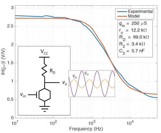
The frequency response of graphene EGFETs was investigated using the common-source (CS) amplifier configuration. In this way graphene EGFET frequency response is investigated while simultaneously demonstrating a graphene EGFET as functional amplifiers for the first time. A 98.99 kΩ resistor was employed as the drain resistor . The operating voltage was approximately 3.3 V and the drain of the graphene EGFET was biased at approximately 150 mV. Graphene EGFETs are not biased at high voltages to avoid undesirable redox reactions at the graphene-electrolyte interface and potential damage to the graphene channel. A small-signal 20 mV p-p sinusoid was superimposed on a DC bias. The DC bias was then manually adjusted to maximize the output and small-signal gain of the amplifier. The optimal bias was found to be to the right of the Dirac point on the graphene I–V curve, which is consistent with Figure 8. This indicates that the graphene EGFET channel is n-type and that the transconductance is positive with respect to the orientation depicted in Figure 5. The frequency of the small-signal input voltage was then swept from 10 Hz to 50 kHz in order to characterize the CS amplifier’s frequency-dependent magnitude response. The CS amplifier transfer function closely resembles the transfer function of the intrinsic graphene EGFET derived in Equation (4). The key exception is that the CS amplifier contains an additional drain resistor at the output, which leads to the CS amplifier transfer function given by Equation (11).
The measured CS amplifier magnitude response was fit to the newly developed small-signal model for graphene EGFETs as shown by Figure 9. The CS amplifier reference schematic is provided as an inset in Figure 10 for convenience. Fitting was achieved using bounded simulating annealing in conjunction with a least squares error function. Transconductance was estimated at 250 μS from the DC characterization data previously obtained for a operating bias of 150 mV. Small-signal model parameters, , , and were extracted as 12.2 kΩ, 3.4 kΩ, and 5.7 nF, respectively. The experimental data verifies the presence of parasitic capacitance , which is responsible for the roll-off in gain. The experimental magnitude response also verifies the presence of resistance at the output, a unique feature in graphene EGFETs stemming from electrolyte solution resistance . Maximum gain, cutoff frequency, and transition frequency were found to be approximately 2.8 V/V, 2.0 kHz, and 7.8 kHz, respectively.
The intrinsic magnitude response of the graphene EGFET is readily computed due to its similarity to the CS amplifier magnitude response (Equations (4) and (11)). Corresponding intrinsic phase response was computed using the extracted parameter values previously listed. A Bode plot for the intrinsic graphene EGFET magnitude and phase response is shown in Figure 10. The maximum intrinsic gain was found to be 3.1 V/V, the cutoff frequency was 1.9 kHz, and the transition frequency occurs at approximately 6.9 kHz. The corresponding equations for intrinsic graphene EGFET magnitude response and phase response are provided by Equations (12) and (13).
It is important to note that the CS amplifier small-signal equivalent circuit model neglects series resistance introduced by contact resistances. Previous work establishes the contact resistance at 6.3 kΩ μm for this graphene EGFET microfabrication process, which translates to a small additional series resistances of approximately 200 Ω per contact [35]. Gated contact resistances are accurately approximated as linear over a small voltage range, which is precisely the case for the small-signal modulation of 20 mVp-p. Including contact resistance in the CS amplifier small-signal equivalent circuit model results in the DC gain described by Equation (14).
and represent the series resistances at the drain and source terminals, respectively. Because and contact resistances and are much less than , Equation (14) reduces to the DC gain previously described in Equation (11). Thus, contact resistances may be safely neglected in small-signal circuit models used to calculate amplifier gain and frequency response.
4.3. Performance Insights and Tradeoffs
Examination of parasitic capacitance provides further insight into the performance tradeoffs affecting graphene EGFET frequency response. Parasitic capacitance occurs between the drain and source. The extracted value of 5.7 nF for is too large to result from the graphene-electrolyte interface capacitance, which was previously approximated at 3 μF/cm2 as detailed in Section 2.1. Given the channel dimensions, the graphene-electrolyte interface contributes approximately 13.5 pF of parasitic gate-drain capacitance.
Figure 11A shows that the drain contact lead accounts for the majority of the parasitic capacitance . Long contact leads are required to connect source and drain regions of the graphene EGFET, which are immersed in an electrolyte droplet, to dry contact pads that must be located further away (i.e., not submerged in electrolyte). A capacitance of 5.2 nF was extracted using EIS for the drain contact lead. This value is roughly equivalent (and consistent) with the 5.7 nF value of extracted using the newly developed small-signal model. Thus, contact lead capacitance greatly hampers graphene EGFET frequency response and motivates the development of smaller area leads.
Figure 11B shows the Au-electrolyte interface capacitance for the exposed metal of the drain region is approximately 7.6 μF/cm2. This is roughly 150% larger than the graphene-electrolyte interface capacitance and contributes approximately 40 nF in parasitic capacitance given the dimensions of the exposed drain metal. This results in an important tradeoff. Recessed channel passivation is known to reduce series resistance and enhance graphene EGFET transconductance performance. Recessed passivation, however, also introduces a parasitic capacitance substantially greater than that of the graphene-electrolyte interface. This motivates tighter misalignment constraints to reduce the metal exposure of the drain region. This finding also motivates development of self-aligned fabrication processes.
Lastly, attention should be drawn to the fact that introduces a pole in the graphene EGFET transfer function and ultimately controls the degree of gain degradation seen at high frequencies. stems from the solution resistance and therefore may be manipulated to a limited extent in many chemical and biological sensing applications. For instance, applications in which graphene EGFETs are employed as ion-selective chemical sensors (e.g., Na+, K+, Cl−, Ca2+) must necessarily vary ion concentrations and therefore solution resistance. Similarly, biological sensing applications provide little control over the cell medium composition and resulting solution resistance. This further motivates the reduction of parasitic capacitances, especially in order to enhance the frequency response of graphene EGFETs.
5. Conclusions
To the extent of our knowledge, this work develops the first small-signal frequency-dependent model for graphene electrolyte-gated field-effect transistors (EGFETs). This was accomplished by incorporating the Randles circuit into the small-signal field-effect transistor model. The newly developed small-signal model was shown to be capable of fitting the experimental data exceptionally well. Extracted parameters from the small-signal model were in good agreement with the parameters independently derived from DC characterization. Thus, two separate methods were employed to extract parameters, both of which yielded similar results. The small-signal model shows that graphene EGFETs contain a unique additional resistive element in series with the parasitic output capacitance. This added resistive element adds a zero to the transfer function causing the graphene EGFET magnitude response to level off at high frequencies. The presence of this additional pole was experimentally verified. All of these reasons attest to the accuracy of the newly developed small-signal model for graphene EGFETs.
This work also employs graphene EGFETs as a common-source amplifier configuration. To the extent of our knowledge, this work demonstrates for the first time, the ability of graphene EGFETs to function effectively as amplifiers providing a gain of 3 V/V. This concretely demonstrates the utility of graphene EGFET sensors in chemical and biological applications.
The majority of the parasitic drain-source capacitance was found to stem from the access lead for the drain. Contributions of the graphene-electrolyte interface and exposed metal drain contact are measured and compared as well. This reveals an important tradeoff in graphene EGFET design. Recessed channel passivation reduces parasitic series resistance and enhances graphene EGFET transconductance. However, recessed channel passivation also necessarily exposes some portion of the source and drain contacts. This increases parasitic capacitances and diminishes the operating frequencies for graphene EGFETs. This motivates the development of self-aligned microfabrication processes for high-performance graphene EGFETs.
This work provides a number of insights into the frequency-dependent small-signal behavior of graphene electrolyte-gated field-effect transistors (EGFETs). As such, it marks a critical step in the development of high-speed chemical and biological sensors based using graphene EGFETs.
Acknowledgments
The authors would like to acknowledge grants from the Office of Naval Research (N00014-12-1-0959, N0014-16-1-2230), the NASA Langley Research Center (NNX14AH11A), and the Army Research Office’s Institute for Soldier Nanotechnologies (W911NF-13-D-0001 T.O.9) for supporting this research.
Author Contributions
Charles Mackin conceived and designed the experiment for measuring the frequency response of graphene EGFETs. He also performed the graphene EGFET fabrication, data analysis, and wrote the paper. Charles Mackin and Elaine McVay jointly developed the frequency-dependent small signal model for graphene EGFETs and conducted experiments. Tomás Palacios advised and funded this work.
Conflicts of Interest
The authors declare no conflict of interest.
References
- Geim, A.K.; Novoselov, K.S. The Rise of Graphene. Nat. Mater. 2007, 6, 183–191. [Google Scholar] [CrossRef] [PubMed]
- Zhu, Y.; Murali, S.; Cai, W.; Li, X.; Suk, J.W.; Potts, J.R.; Ruoff, R.S. Graphene and Graphene Oxide: Synthesis, Properties, and Applications. Adv. Mater. 2010, 22, 3906–3924. [Google Scholar] [CrossRef] [PubMed]
- Castro Neto, A.H.; Guinea, F.; Peres, N.M.R.; Novoselov, K.S.; Geim, A.K. The Electronic Properties of Graphene. Rev. Mod. Phys. 2009, 81, 109–162. [Google Scholar] [CrossRef]
- Soldano, C.; Mahmood, A.; Dujardin, E. Production, Properties and Potential of Graphene. Carbon N. Y. 2010, 48, 2127–2150. [Google Scholar] [CrossRef]
- Petrone, N.; Dean, C.R.; Meric, I.; van der Zande, A.M.; Huang, P.Y.; Wang, L.; Muller, D.; Shepard, K.L.; Hone, J. Chemical Vapor Deposition-Derived Graphene with Electrical Performance of Exfoliated Graphene. Nano Lett. 2012, 12, 2751–2756. [Google Scholar] [CrossRef] [PubMed]
- Kim, K.S.; Zhao, Y.; Jang, H.; Lee, S.Y.; Kim, J.M.; Kim, K.S.; Ahn, J.-H.; Kim, P.; Choi, J.-Y.; Hong, B.H. Large-Scale Pattern Growth of Graphene Films for Stretchable Transparent Electrodes. Nature 2009, 457, 706–710. [Google Scholar] [CrossRef] [PubMed]
- Bae, S.; Kim, H.; Lee, Y.; Xu, X.; Park, J.-S.; Zheng, Y.; Balakrishnan, J.; Lei, T.; Kim, H.R.; Song, Y.I.; et al. Roll-to-roll production of 30-inch graphene films for transparent electrodes. Nat. Nanotechnol. 2010, 5, 574–578. [Google Scholar] [CrossRef] [PubMed]
- Stöberl, U.; Wurstbauer, U.; Wegscheider, W.; Weiss, D.; Eroms, J. Morphology and Flexibility of Graphene and Few-Layer Graphene on Various Substrates. Appl. Phys. Lett. 2008, 93, 51906. [Google Scholar] [CrossRef]
- Xu, Y.; Wang, Y.; Liang, J.; Huang, Y.; Ma, Y.; Wan, X.; Chen, Y. A Hybrid Material of Graphene and Poly (3,4-ethyldioxythiophene) with High Conductivity, Flexibility, and Transparency. Nano Res. 2009, 2, 343–348. [Google Scholar] [CrossRef]
- Lee, C.; Wei, X.; Kysar, J.W.; Hone, J. Measurement of the Elastic Properties and Intrinsic Strength of Monolayer Graphene. Science 2008, 321, 385–388. [Google Scholar] [CrossRef] [PubMed]
- Zhou, M.; Zhai, Y.; Dong, S. Electrochemical Sensing and Biosensing Platform Based on Chemically Reduced Graphene Oxide. Anal. Chem. 2009, 81, 5603–5613. [Google Scholar] [CrossRef] [PubMed]
- Elias, D.C.; Nair, R.R.; Mohiuddin, T.M.G.; Morozov, S.V.; Blake, P.; Halsall, M.P.; Ferrari, A.C.; Boukhvalov, D.W.; Katsnelson, M.I.; Geim, A.K.; et al. Control of Graphene’s Properties by Reversible Hydrogenation: Evidence for Graphane. Science 2009, 323, 610–613. [Google Scholar] [CrossRef] [PubMed]
- Shao, Y.; Wang, J.; Wu, H.; Liu, J.; Aksay, I.A.; Lin, Y. Graphene Based Electrochemical Sensors and Biosensors: A Review. Electroanalysis 2010, 22, 1027–1036. [Google Scholar] [CrossRef]
- Brownson, D.A.C.; Kampouris, D.K.; Banks, C.E. Graphene Electrochemistry: Fundamental Concepts through to Prominent Applications. Chem. Soc. Rev. 2012, 41, 6944–6976. [Google Scholar] [CrossRef] [PubMed]
- Ji, H.; Zhao, X.; Qiao, Z.; Jung, J.; Zhu, Y.; Lu, Y.; Zhang, L.L.; MacDonald, A.H.; Ruoff, R.S. Capacitance of Carbon-Based Electrical Double-Layer Capacitors. Nat. Commun. 2014, 5, 3317. [Google Scholar] [CrossRef] [PubMed]
- Hess, L.H.; Seifert, M.; Garrido, J.A. Graphene Transistors for Bioelectronics. Proc. IEEE 2013, 101, 1780–1792. [Google Scholar] [CrossRef]
- Hess, L.H.; Hauf, M.V.; Seifert, M.; Speck, F.; Seyller, T.; Stutzmann, M.; Sharp, I.D.; Garrido, J.A. High-Transconductance Graphene Solution-Gated Field Effect Transistors. Appl. Phys. Lett. 2011, 99, 33503. [Google Scholar] [CrossRef]
- Xia, J.; Chen, F.; Li, J.; Tao, N. Measurement of the Quantum Capacitance of Graphene. Nat. Nanotechnol. 2009, 4, 505–509. [Google Scholar] [CrossRef] [PubMed]
- Mackin, C.; Hess, L.H.; Hsu, A.; Song, Y.; Kong, J.; Garrido, J.A.; Palacios, T. A Current–Voltage Model for Graphene Electrolyte-Gated Field-Effect Transistors. IEEE Trans. Electron Devices 2014, 61, 3971–3977. [Google Scholar] [CrossRef]
- Meric, I.; Han, M.Y.; Young, A.F.; Ozyilmaz, B.; Kim, P.; Shepard, K.L. Current Saturation in Zero-Bandgap, Top-Gated Graphene Field-Effect Transistors. Nat. Nanotechnol. 2008, 3, 654–659. [Google Scholar] [CrossRef] [PubMed]
- Umoh, I.J.; Kazmierski, T.J.; Al-Hashimi, B.M. A Dual-Gate Graphene FET Model for Circuit Simulation—SPICE Implementation. IEEE Tran. Nanotechnol. 2013, 12, 427–435. [Google Scholar] [CrossRef]
- Fregonese, S.; Magallo, M.; Maneux, C.; Happy, H.; Zimmer, T. Scalable Electrical Compact Modeling for Graphene FET Transistors. IEEE Trans. Nanotechnol. 2013, 12, 539–546. [Google Scholar] [CrossRef]
- Ryzhii, V.; Ryzhii, M.; Satou, A.; Otsuji, T.; Kirova, N. Device Model for Graphene Bilayer Field-Effect Transistor. J. Appl. Phys. 2009, 105, 104510. [Google Scholar] [CrossRef]
- Wang, H.; Member, S.; Hsu, A.; Kong, J.; Antoniadis, D.A.; Palacios, T. Compact Virtual-Source Current–Voltage Model for Top- and Back-Gated Graphene Field-Effect Transistors. IEEE Trans. Electron Devices 2011, 58, 1523–1533. [Google Scholar] [CrossRef]
- Jiménez, D. Explicit Drain Current, Charge and Capacitance Model of Graphene Field-Effect Transistors. IEEE Trans. Electron Devices 2011, 58, 4377–4383. [Google Scholar] [CrossRef]
- Hess, L.H.; Jansen, M.; Maybeck, V.; Hauf, M.V.; Seifert, M.; Stutzmann, M.; Sharp, I.D.; Offenhäusser, A.; Garrido, J.A. Graphene Transistor Arrays for Recording Action Potentials from Electrogenic Cells. Adv. Mater. 2011, 23, 5045–5049. [Google Scholar] [CrossRef] [PubMed]
- Viswanathan, S.; Narayanan, T.N.; Aran, K.; Fink, K.D.; Paredes, J.; Ajayan, P.M.; Filipek, S.; Miszta, P.; Tekin, H.C.; Inci, F.; et al. Graphene-protein field effect biosensors: Glucose sensing. Mater. Today 2015, 18, 513–522. [Google Scholar] [CrossRef]
- Distante, C.; Leo, M.; Siciliano, P.; Persaud, K.C. On the study of feature extraction methods for an electronic nose. Sens. Actuators B Chem. 2002, 87, 274–288. [Google Scholar] [CrossRef]
- Smyth, H.; Cozzolino, D. Instrumental methods (Spectroscopy, Electronic Nose, and Tongue) as tools to predict taste and aroma in beverages: Advantages and limitations. Chem. Rev. 2013, 113, 1429–1440. [Google Scholar] [CrossRef] [PubMed]
- Manickam, A.; Johnson, C.A.; Kavusi, S.; Hassibi, A. Interface design for CMOS-integrated Electrochemical Impedance Spectroscopy (EIS) biosensors. Sensors 2012, 12, 14467–14488. [Google Scholar] [CrossRef] [PubMed]
- Shannon, C.E. Communication in the Presence of Noise. Proc. IRE 1949, 37, 10–21. [Google Scholar] [CrossRef]
- Kilic, M.; Bazant, M.; Ajdari, A. Steric Effects in the Dynamics of Electrolytes at Large Applied Voltages. I. Double-layer Charging. Phys. Rev. E 2007, 75, 21502. [Google Scholar] [CrossRef] [PubMed]
- Schwierz, N.; Horinek, D.; Netz, R.R. Reversed Anionic Hofmeister Series: The Interplay of Surface Charge and Surface Polarity. Langmuir ACS J. Surf. Colloids 2010, 26, 7370–7379. [Google Scholar] [CrossRef] [PubMed]
- Birner, S. Modeling of Semiconductor Nanostructures and Semiconductor—Electrolyte Interfaces. Ph.D. Thesis, Technical University Munich, Munich, Germany, 2011. [Google Scholar]
- Mackin, C.; Palacios, T. Large-scale sensor systems based on graphene electrolyte-gated field-effect transistors. Analyst 2016, 141, 2704–2711. [Google Scholar] [CrossRef] [PubMed]
- Martin, J.; Akerman, N.; Ulbricht, G.; Lohmann, T.; Smet, J.H.; von Klitzing, K.; Yacoby, A. Observation of Electron–Hole Puddles in Graphene using a Scanning Single-Electron Transistor. Nat. Phys. 2007, 4, 144–148. [Google Scholar] [CrossRef]
- Adam, S.; Hwang, E.H.; Galitski, V.M.; Das Sarma, S. A Self-Consistent Theory for Graphene Transport. Proc. Natl. Acad. Sci. USA 2007, 104, 18392–18397. [Google Scholar] [CrossRef] [PubMed]
- Franceschetti, D.R.; Macdonald, J.R. Small-Signal AC Response Theory for Electrochromic Thin Films. J. Electrochem. Soc. 1982, 129, 1754–1756. [Google Scholar] [CrossRef]
- Janek, R.P.; Fawcett, W.R.; Ulman, A. Impedance Spectroscopy of Self-Assembled Monolayers on Au(111): Sodium Ferrocyanide Charge Transfer at Modified Electrodes. Langmuir 1998, 14, 3011–3018. [Google Scholar] [CrossRef]
- Suk, J.W.; Kitt, A.; Magnuson, C.W.; Hao, Y.; Ahmed, S.; An, J.; Swan, A.K.; Goldberg, B.B.; Ruoff, R.S. Transfer of CVD-Grown Monolayer Graphene onto Arbitrary Substrates. ACS Nano 2011, 5, 6916–6924. [Google Scholar] [CrossRef] [PubMed]
Figure 1.
Measured top-gate capacitance as a function of potential using electrochemical impedance spectroscopy. CTOP,EXP (dotted red) is the measured top-gate capacitance, CEDL,EFF (dash-dot yellow) is the effective electric double layer capacitance, CQ (dashed purple) is the quantum capacitance, and CTOP,SIM (blue) is the simulated top-gate capacitance. CTOP,SIM consists of the effective double layer capacitance in series with the graphene quantum capacitance.

Figure 2.
Graphene electrolyte-gated field-effect transistors (EGFET) with recessed top-gate capacitance due to non-self-aligned source/drain passivation. The gate voltage is applied using a reference electrode.
Figure 2.
Graphene electrolyte-gated field-effect transistors (EGFET) with recessed top-gate capacitance due to non-self-aligned source/drain passivation. The gate voltage is applied using a reference electrode.

Figure 3.
Schematic representation of the simplified Randles circuit commonly used to model electrode-electrolyte interfaces.
Figure 3.
Schematic representation of the simplified Randles circuit commonly used to model electrode-electrolyte interfaces.

Figure 4.
Graphene EGFET small-signal models depicting gate-source and drain-source capacitances and resistances using the simplified Randles circuit model.
Figure 4.
Graphene EGFET small-signal models depicting gate-source and drain-source capacitances and resistances using the simplified Randles circuit model.

Figure 5.
Final graphene EGFET small-signal model after application of the Miller theorem.

Figure 6.
(a) Mesa etched graphene after removal of the bilayer MMA/SPR700 resist stack and (b) completely fabricated graphene EGFET with lead passivation using a recessed SU-8 layer.
Figure 6.
(a) Mesa etched graphene after removal of the bilayer MMA/SPR700 resist stack and (b) completely fabricated graphene EGFET with lead passivation using a recessed SU-8 layer.

Figure 7.
Graphene EGFET vs. for different applied values.

Figure 8.
Intrinsic voltage gain as a function of and as calculated from DC characterization.

Figure 9.
Fit of experimental graphene EGFET magnitude response with newly developed small-signal model for graphene EGFETs.
Figure 9.
Fit of experimental graphene EGFET magnitude response with newly developed small-signal model for graphene EGFETs.

Figure 10.
Bode plot depicting the intrinsic graphene EGFET magnitude and phase response.

Figure 11.
Electrochemical impedance spectroscopy (EIS) of (a) the drain contact lead with the graphene channel removed, and (b) the Au-electrolyte interface capacitance. Measurements were taken in aqueous 100 mM NaCl.
Figure 11.
Electrochemical impedance spectroscopy (EIS) of (a) the drain contact lead with the graphene channel removed, and (b) the Au-electrolyte interface capacitance. Measurements were taken in aqueous 100 mM NaCl.

© 2018 by the authors. Licensee MDPI, Basel, Switzerland. This article is an open access article distributed under the terms and conditions of the Creative Commons Attribution (CC BY) license (http://creativecommons.org/licenses/by/4.0/).
Share and Cite
MDPI and ACS Style
Mackin, C.; McVay, E.; Palacios, T. Frequency Response of Graphene Electrolyte-Gated Field-Effect Transistors. Sensors 2018, 18, 494. https://doi.org/10.3390/s18020494
AMA Style
Mackin C, McVay E, Palacios T. Frequency Response of Graphene Electrolyte-Gated Field-Effect Transistors. Sensors. 2018; 18(2):494. https://doi.org/10.3390/s18020494
Chicago/Turabian StyleMackin, Charles, Elaine McVay, and Tomás Palacios. 2018. "Frequency Response of Graphene Electrolyte-Gated Field-Effect Transistors" Sensors 18, no. 2: 494. https://doi.org/10.3390/s18020494
Note that from the first issue of 2016, this journal uses article numbers instead of page numbers. See further details here.