Temporal Noise Analysis of Charge-Domain Sampling Readout Circuits for CMOS Image Sensors †


1
Electronic Instrumentation Laboratory, Delft University of Technology, 2628 CD Delft, The Netherlands
2
Harvest Imaging, 3960 Bree, Belgium
*
Author to whom correspondence should be addressed.
†
This paper is an expanded version of our paper published in Ge, X.; Theuwissen, A. A 0.5 e- rms Temporal-Noise CMOS Image Sensor with Charge-Domain CDS and Period-Controlled Variable Conversion-Gain. In Proceedings of the 2017 International Image Sensor Workshop, Hiroshima, Japan, 30 May–2 June 2017.
Sensors 2018, 18(3), 707; https://doi.org/10.3390/s18030707
Submission received: 21 November 2017
/
Revised: 28 January 2018
/
Accepted: 13 February 2018
/
Published: 27 February 2018
(This article belongs to the Special Issue Special Issue on the 2017 International Image Sensor Workshop (IISW))
Abstract
:This paper presents a temporal noise analysis of charge-domain sampling readout circuits for Complementary Metal-Oxide Semiconductor (CMOS) image sensors. In order to address the trade-off between the low input-referred noise and high dynamic range, a Gm-cell-based pixel together with a charge-domain correlated-double sampling (CDS) technique has been proposed to provide a way to efficiently embed a tunable conversion gain along the read-out path. Such readout topology, however, operates in a non-stationery large-signal behavior, and the statistical properties of its temporal noise are a function of time. Conventional noise analysis methods for CMOS image sensors are based on steady-state signal models, and therefore cannot be readily applied for Gm-cell-based pixels. In this paper, we develop analysis models for both thermal noise and flicker noise in Gm-cell-based pixels by employing the time-domain linear analysis approach and the non-stationary noise analysis theory, which help to quantitatively evaluate the temporal noise characteristic of Gm-cell-based pixels. Both models were numerically computed in MATLAB using design parameters of a prototype chip, and compared with both simulation and experimental results. The good agreement between the theoretical and measurement results verifies the effectiveness of the proposed noise analysis models.
1. Introduction
Advanced imaging systems for high-end applications, such as scientific and medical imaging, demand high-sensitivity CMOS image sensors (CIS). The noise performance of such CIS usually determines the ultimate detection sensitivity of the overall imaging system. However, CIS generally suffer from high temporal noise, which is typically measured by the minimum number of detectable electrons (e−rms) at the input of the pixel.
To improve the temporal noise performance of the CIS, a variety of solutions have been proposed. An effective approach is to implement a high-gain stage at the column-level, as well as to minimize the capacitance associated with the floating diffusion (FD) node at the pixel-level. By virtue of the high conversion gain (CG) along the signal path, such an approach is capable of effectively reducing the input-referred noise of each pixel. Image sensors based on this architecture have been demonstrated in serval prior designs [1,2,3,4,5,6,7,8,9,10,11], which exhibited excellent image capturing performance along with a very impressive photon-counting capability in respect of the superior noise performance. Nevertheless, the use of a fixed high-gain amplification in the pixel, either in the charge domain or the voltage domain, inevitably leads to degradation of the dynamic range (DR), thus resulting in undesired contrast loss in the final image.
To solve this problem, a charge-domain sampling pixel readout circuit based on trans-conductance (Gm)-cells has been proposed in [12,13] as an alternative to the conventional voltage-domain implementation based on source followers (SF). The linear-charging characteristic of Gm-cells enables the implementation of a variable voltage gain at the pixel level, by means of controlling the length of the charging period. As such, the CG of the overall read-out path can be programmed according to the specific application of the CIS, without the need for reconstructing or replacing the hardware. Therefore, the proposed pixel structure is able to overcome the trade-off between the low input-referred noise and high DR.
While the operational principle and implementation details of the Gm-cell-based pixel have been described in [12,13], this paper focuses on its noise characteristic. Compared to its counterpart based on source followers, a Gm-cell-based pixel operates in a non-stationary large-signal [14] manner, i.e., its bias condition changes as a function of the operating time. Therefore, the traditional temporal noise analysis method based on steady-state small-signal models does not readily apply to a Gm-call-based pixel. In view of the above issues, we propose an exact temporal noise model to guide the analysis and design of a Gm-cell-based pixel. The effectiveness of this model has been successfully verified with both simulation and prototype measurement results.
This paper is organized as follows. In Section 2, the operation principles of a Gm-cell-based pixel are briefly reviewed. Section 3 introduces the theoretical fundamentals used for the noise analysis and presents the details of the noise analysis model. Section 4 compares the analysis model with experimental results derived from simulations and measurements. Finally, a conclusion is given in Section 5.
2. Operating Principle and Implementation of a Gm-Cell-Based Pixel
2.1. Concept of Gm-Cell-Based Pixel
A simplified schematic of the Gm-cell-based pixel is shown in Figure 1a. Its basic architecture consists of a pinned-photodiode (PPD), a Gm-cell and a sample-and-hold (S/H) capacitor. Similar to [1], a single-ended cascode common-source topology has been chosen as the proposed pixel-level Gm-cell in consideration of the fill factor limitation. In addition, the column-parallel readout path has been implemented with the correlated-double sampling (CDS) S/H switches and capacitor banks for the sake of the simplicity of this proof-of-concept design.
Figure 1b illustrates the associated basic operation timing diagram. In contrast to conventional voltage-sampling pixels, the voltage on the FD node, VFD, is first converted to a signal-dependent current (Ipix) by the Gm-cell, rather than buffered by a unity-gain source follower. Ipix is then integrated onto the S/H capacitor (CS/H) with a programmable duration Tch, at the end of which the voltage stored on CS/H is readout as a representative of VFD. After that, CS/H is reset by the switch RST to clear the charge before the next sampling phase. Such sampling process essentially operates in the charge-domain, while the pixel output signal is still in the voltage domain. Its transfer function is:
where gm is the trans-conductance of MCS, TS is the sampling period and n is an integer.
Equation (1) describes a boxcar sampling process [15], which can be interpreted as the convolution integral of VFD and a rectangular time window with a height of gm/CS/H and a width of Tch. Its transfer function can be written as [16]:
whose ideal magnitude transfer function can be expressed as a sinc-type low-pass filter with a defined DC gain:
Notice that the sampled voltage has been hold with zero-order hold (ZOH) process [17] after the charging phase, the ZOH model has been included as one term of the overall charge-domain sampling transfer function, which is shown below:
where TZOH is the sampling period, which is equal to Tch in the case of charge-domain sampling.
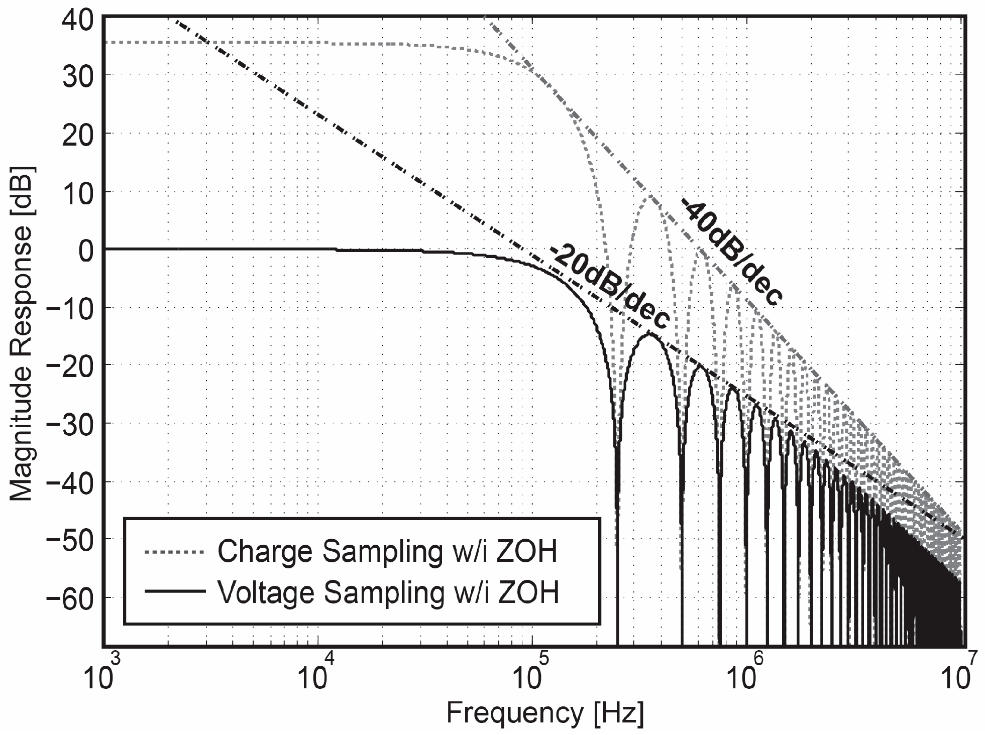
Intuitively, in comparison to a voltage-domain sampling readout path, a charge-domain sampling circuit introduces an additional first-order sinc-type low-pass filter prior to the discrete-time sampler, resulting in a twice steeper roll-off in the overall transfer function, as shown in Figure 2. The extra sinc-type filter features frequency notches locating at integer multiples of 1/Tch.
The above analysis reveals some important advantages of Gm-cell-based pixels for low-noise design: (1) A programmable voltage gain and −3 dB bandwidth can be realized by tuning the length of the charging window. Increasing Tch not only boosts the voltage gain, but also narrows down the readout bandwidth, both of which are beneficial for suppressing the pixel-level input-referred noise. (2) The charge-sampling process provides an additional anti-aliasing filtering, leading to further compression of the high-frequency noise components. Both features are taken into account in the following noise analysis (Section 3).
2.2. Periodic Filtering Model of the Charge-Domain CDS
CDS is widely used in CIS for low-frequency noise reduction. By subtracting the reset level sampled at Trst from the signal level sampled Tsig, both the offset and the flicker noise could be effectively suppressed. The effect of the CDS noise canceller can be characterized as a discrete-time (DT) high-pass filtering operation, as analysed in [18]. The transfer function of HCDS(f) is given by
where T0 is the sampling interval between Trst and Tsig. A behavioral model of the Gm-cell-based pixel with charge-domain CDS is depicted in Figure 3. As two distinct filtering functions, namely, a continuous-time (CT) sinc low-pass filter HWI(f) [19] and a DT high-pass filter HCDS(f) are realized simultaneously, the overall transfer function of the charge-domain CDS can be written as
Compared to a corresponding voltage-domain CDS transfer function, which has an equal −3 dB bandwidth, the charge-domain CDS introduces one additional group of notches. As shown by simulations in Figure 4, one group of notch frequencies is located at k/Tch, owing to the charge-sampling sinc-type filter (sinc(πfTch)), while the other group is placed at k/T0, owing to the sinc function effect (sin(πfT0) of the CDS operation [20]. The joint effect of sinc(πfTch) and sin(πfTch) increases the depth of the notches thus further improving the attenuation in the stop band. As such, the charge-domain CDS not only helps in reducing the low-band noise, but also provides a greater extent of attenuation on high-frequency noise components, in comparison with the voltage-domain CDS which only features first-order low-pass filtering.
3. Noise Analysis of a Gm-Cell-Based Pixel
3.1. Nonstationary Noise Theory Analysis
Temporal noise analysis on conventional CIS readout circuits is established based on the fact that the pixel-level SF operates in the steady-state [21]. As shown in Figure 5a, in the process of the voltage-domain sampling with an exponential settling behavior, the statistics properties of the temporal noise do not vary as a function of time and can be well represented by its time-averaged root-mean-square (RMS) value. However, this prerequisite is not valid for Gm-cell-based pixels. A time-domain plot of the voltage on the S/H capacitor with superimposed random noise is conceptually shown in Figure 5b. As explained in Section II, the final output signal on the S/H capacitor is obtained through a charging process. Given the fact that the proposed read-out topology works with a large signal behavior throughout its operation, the standard deviation of the voltage distribution and hence the RMS value of the noise is no longer static with time. Therefore, the conventional noise analysis method based on steady-state models is not appropriate for Gm-cell-based pixels along with its read-out path. To quantitatively analyze the nonstationary noise, a time-domain linear analysis approach, based on the autocorrelation of nonstationary random process, has been described in [14,22]. Here, we apply a similar approach to evaluate the temporal noise characteristic of Gm-cell-based pixels.
Noise in the time-domain represents the variance of a random process, which can be derived from its autocorrelation as a function of time [23]. Suppose that the time-domain representatives of the input and output noise are X(t) and Y(t) respectively, the autocorrelation of the input noise between two time points ( and ) is Rxx(t1, t2) and the time-domain impulse response of the pixel readout circuit is hp(t). Thus, the autocorrelation of the output noise can be derived from time-domain convolutions [14]:
The variance of Y(t) as a function of the autocorrelation is:
Equations (7) and (8) serve as the fundamental for the time-domain analysis of Gm-cell-based pixels. As can be seen, in order to investigate the output noise in the time-domain, all that is required is the input noise autocorrelation functions of different noise sources, as well as the impulse response from the pixel input voltage (VFD) to its output. During the charging phase of a Gm-cell-based pixel, both the thermal noise and flicker noise of the Gm-cell contribute to the overall output noise. In addition, the kTC noise caused by the column-level switch also affords a part of noise in the reset phase. Therefore, in the following discussions their contributions will be investigated separately.
3.2. Equivalent Small Signal Model and Noise Gain
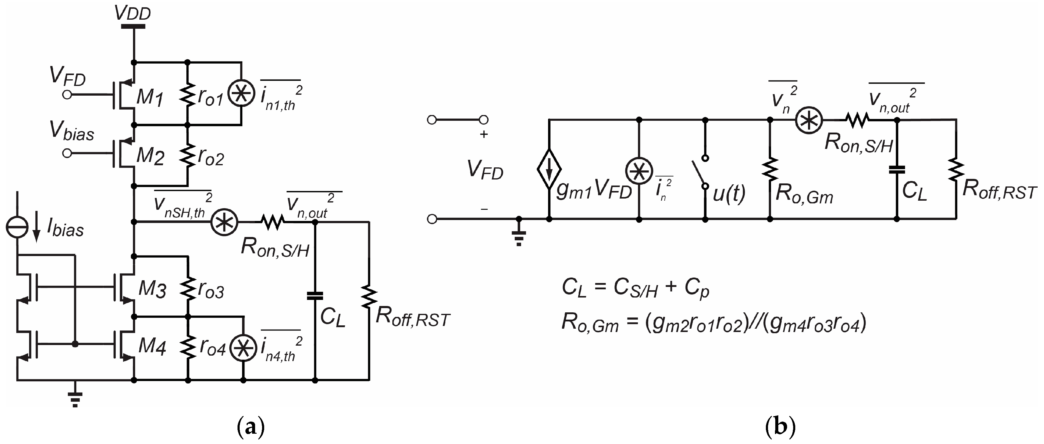
Although a Gm–C integrator works in a large-signal behavior throughout its charging phase, its small-signal model at the completion moment of the sampling response can still be utilized for a first-order noise analysis, due to the fact that only the noise power at that point has impacts on the final decision. Figure 6 shows the noise model and the equivalent small signal model of the readout path of a Gm-cell-based pixel.
In order to facilitate the noise optimization, the mentioned output noise power needs to be referred to the FD node. For this purpose, the noise gain of the Gm-cell-based pixel must be first calculated.
According to [14], the noise gain of an integrator-like Gm-cell can be determined by the ratio of voltage slopes at the output and input ports:
The input signal VFD of the Gm-cell during the charging phase can be assumed as a slow ramp and is given as:
where K is the input voltage magnitude. The time-domain response of a Gm-cell to a step ramp input is given by:
where A0 = gm1ROUT is the DC gain of the Gm-cell at the steady-state, τ is the time constant of the Gm–C integrator, Ro,Gm is the output impedance of the Gm-cell, Ron,S/H is the on-resistance of switch SH, the value of which is much smaller than Ro,G, Roff,RST is the off-resistance of switch RST (RSTr and RSTs). Thus, the final noise gain of the Gm-cell can be described by the following expression:
Note that this result can be simplified into two special cases:
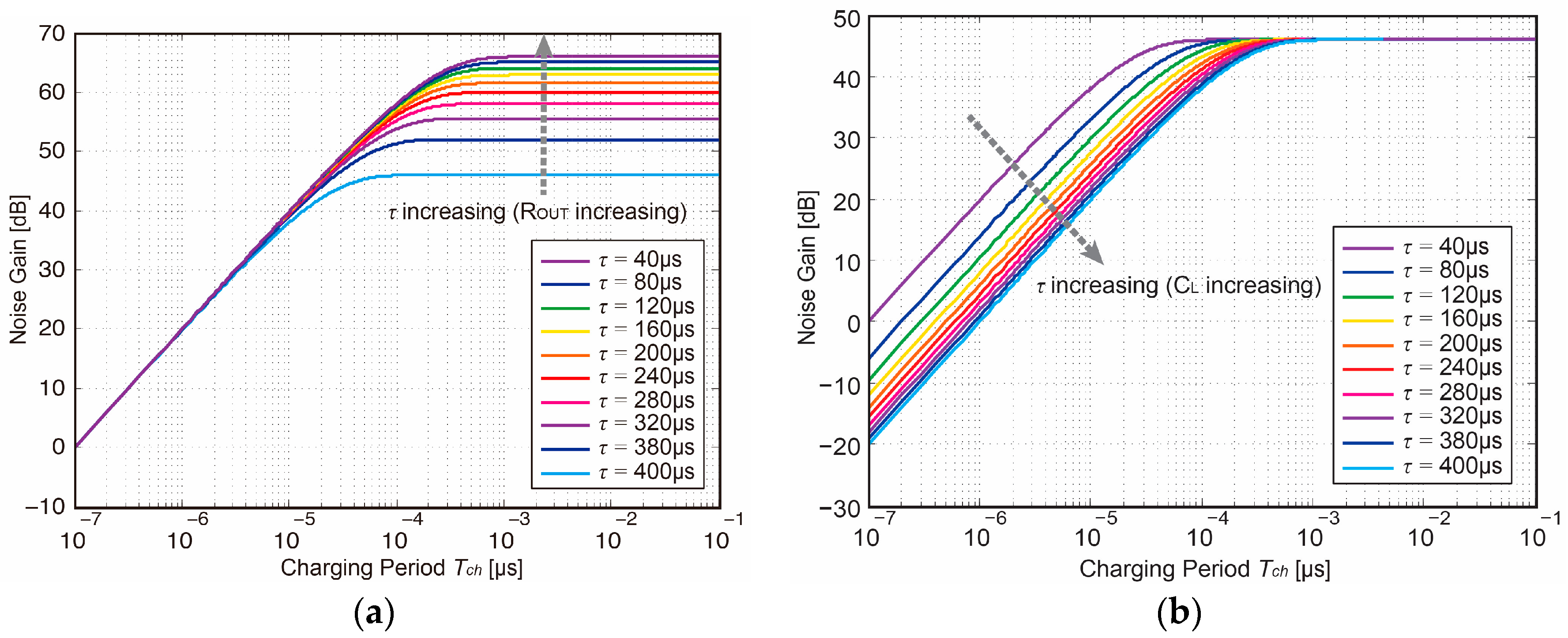
To be more precise, a plot showing the variation of the noise gain factor as a function of charging period Tch with a wide range of time constant τ. As revealed in Figure 7a and Equation (13a), with a constant Tch and the time-boundary Tch >> τ, the noise gain increases as τ and ROUT increasing, which showing the steady-state noise gain characteristic of a broadband amplifier. Figure 7b and Equation (13b) shows an integrator-like noise gain with the time-boundary Tch >> τ resulting from the charge-sampling process as explained in [2], which is inversely proportional to τ and CL with a constant Tch.
3.3. Noise Model of Charging Phase
3.3.1. Thermal Noise
In a Gm-cell small signal model, the impulse response from the noise current source to the output voltage Vout, which is given by [14]:
where CS/H is the loading S/H capacitance, Cp is the parasitic capacitance of the column net, Ro,Gm is the output impedance of the Gm-cell, τ is the time constant of this Gm–C integrator and u(t) is the noise current unit step input.
Consider a white noise unit step input un(t), the autocorrelation function of the thermal noise source is a Dirac delta function with an amplitude equal to its double-sided power spectral density (PSD) [23]:
where Sth,n is the equivalent single-sided temporal noise PSD. According to Figure 6, the noise sources include the equivalent current noise source in from the pixel-level Gm-cell and the equivalent voltage noise source vn from the column-level sample-and-hold switch SH (SHr and SHs). Thus, Sth,n can be modelled as:
where gn = 2(gm1 + gm4)/3 is the equivalent noise trans-conductance of in, k = 1.3807 × 10⁻²³ J/K is the Boltzmann constant and T is absolute temperature in Kelvin.
By substituting Equations (14) and (15) into Equations (7) and (8), we obtain the variance of the output voltage due to the time-variant thermal noise, as given by:
with the aid of Equation (16), the above integral can be solved as:
In a charge sampling circuit, only the noise at the instant of the sampling completion (Tch) has impact on the final readout noise. Accordingly, the concerned output thermal noise power of a Gm-cell-based pixel can be evaluated as:
On the basis of Equations (12) and (19), the input thermal noise power can be derived by:
As Equation (20) contains a hyperbolic function of the ratio of the charging time Tch and time constant τ, the time limits Tch >> τ and Tch << τ are thus of interest. Figure 8 showing the variation of the input thermal noise power with a wide range of time constant τ. With a fixed Tch, the input-referred thermal noise decreases as τ increases at the time-boundary of Tch << τ. Its noise behavior is identical with the input-referred thermal noise power in common single-pole steady-state systems. On the other hand, if Tch << τ, the input-referred thermal noise linearly reduces as Tch gets longer for a given τ. Within this region, the thermal noise becomes Tch-dependent and behaves as an integrator-like noise. As such, this interesting characteristic offers an orientation to the thermal noise estimation in the specific design of Gm-cell-based pixels.
3.3.2. Flicker Noise
Flicker noise in CIS refers to those noise sources whose PSD is inversely proportional to the frequency. The flicker noise PSD sourced from the input MOS transistor of the Gm-cell can be modeled as:
where K is a process-dependent constant, Cox is the unit oxide capacitance of the MOS gate, and A is the channel area. In contrast to thermal noise, the time-domain response of flicker noise is a nonstationary process [22].
where is the impulse response of an ideal 1/f noise-shaping filter:
Here, fc is the corner frequency of the flicker noise, which is relevant to the process and transistor parameter:
Based on Equations (23)–(25), the autocorrelation of flicker noise can be expressed as:
Equation (26) appears as a divergent integral function of time [24,25,26,27] and does not have a finite limit. To address this issue, characterization of the flicker noise is often reasonably limited to a finite length of observation time window [24] (or a limited bandwidth in the frequency domain [23]). The minimum of this time window (tmin) is defined by the reciprocal of the upper limit of the concerned frequency range, i.e., the flicker corner frequency (fc), while the total operation time of the readout circuit (top) determines the maximum. Based on this approximation, the autocorrelation of flicker noise can be written as [23]:
By substituting Equations (14) and (27) into Equations (6) and (7), the variance of the pixel output voltage owing to flicker noise can be expressed as:
Similarly, the output flicker noise at the sampling instant is evaluated at Tch:
However, the integral in Equation (28) does not have an analytic solution. Therefore, Equations (28) and (29) must be numerically computed in MATLAB to get a quantitative evaluation of the flicker noise power. Note that top should be assigned with a sufficiently large value to ensure the accuracy of approximation (typically around one hour [22]). Take the CDS effect into consideration, the impulse response of the ideal 1/f noise-shaping filter are assumed as h1/f(Tch) and h1/f(T0 + 2Tch). Therefore, the autocorrelation of the flicker noise with CDS is given as:
where T0 is the interval period between two samples (reset level and signal level) which is assumed as T0 = Tch + 1 µs. Consequently, the output flicker noise power after CDS can be defined by:
As a brief proof, Figure 9 numerically plot the flicker noise output power as a function of charging time Tch. In contrast to thermal noise output power whose value reaches steady-state until Tch ≈ 2τ, flicker noise is continuously accumulated with an increasing Tch, which agrees with the theoretical analysis of the flicker noise in frequency domain.
According to our circuit level simulations, the corner frequency fc is around 500 kHz, which is higher than the equivalent noise bandwidth of the proposed circuit, and thus the flicker noise obviously appears even beyond the noise bandwidth. As a result, the input-referred flicker noise is highly dependent on Tch and it is effectively reduced through increasing Tch. On the contrary, as the Gm-cell enters into the steady-state region when Tch gets longer. The input-referred flicker begins to increase due to a constant noise gain and noise bandwidth.
3.4. Noise Model of Discharging Phase
In order to segregate the sampling operations between two adjacent frames, the S/H capacitor is discharged by switching on RST (RSTr and RSTs) before the next new frame. As the switch operation during this process is considered to have reached stationary levels with an exponential settling behavior, the noise is therefore exhibit as the steady-state. By using the first-order low-pass filter transfer function, the thermal noise power caused by switch RST is calculated as:
where Ron,RST is the on-resistance of switch RST. Different from the voltage-domain sampling circuit, the charging phase follows the switch off of RST. As a consequence, part of the noise charge on CL is discharged in the charging phase with a non-stationary random process and thus the resulting noise power from RST is given as:
where the term represent the amplitude degrading during the charging phase. The value of the kTC noise from the discharging phase are also numerically investigated, with results presented in Figure 10a,b.
3.5. Overall Input-Referred Noise
Consequently, the overall input-referred temporal noise power of a Gm-cell-based pixel can be calculated by:
The combination of formulas (20), (31) and (33) provides an effective way to predict and calculate the temporal noise power of Gm-cell-based pixels in the time domain. Given the fact that the proposed circuit operates as a Gm–C integrator, Tch should be settled with the range of Tch << τ. Applying the device parameters used for the design of the CIS chip as listed in Table 1, the noise components of the readout circuits and the resulting total noise are calculated in MATLAB, which is shown in Section 4 as a comparison of measurement result.
4. Implementation and Experimental Results
The test sensor with the proposed pixel architecture has been fabricated in a 0.18 µm 1P4M standard CIS process technology. The test pixels have been divided into six sub-groups, each of which includes 20 (H) × 32 (V) pixels and features the same pixel pitch of 11 µm. For flexibility, the digital logic, which implements the charging clocks Tch and other operating clocks are realized off-chip. By performing these double charging processes, the resulting voltage level Vreset and Vsignal are held on Cr and Cs respectively and are sequentially readout from the CIS chip via multiplexers and output buffers. An off-chip 16-bit ADC with an LSB of 30 µV has been implemented on the PCB to convert the analog output voltage levels into digital signal. The voltage subtraction of the reset level and the signal level (Vreset − Vsignal) is then performed in the digital domain with the aid of an NI-IMAQ (National Instruments–Vision Acquisition Software) 16.2. In this way, we realize the CDS in digital domain and obtain the period-controlled amplified video signal Vsignal − Vreset with the charge-domain CDS.
A critical parameter for the evaluation of the temporal noise is the conversion gain. The pixel-level conversion gain CGtot associated with the period-controlled function has been measured by using the photon transfer curve (PTC) measurement technique. Figure 11 shows the measured conversion gain CGtot = CGFD × Apix of the fabricated Gm-cell-based pixel, where CGFD is the conversion gain at the FD node. To separately investigate the gain factor Apix of the charge-sampling pixel, we also measured the CGFD of a unity-gain pMOS SF-based 4T-pixel [28] as a reference for comparison, whose the FD node is laid out with the same area as the proposed pixel. Note that the CGFD of the SF-based pixel is measured as 55 μV/e−, which indicates that the nominal value Apix of the charge-sampling pixel is around ×30. The measurement results show that CGtot can be programmable from 50 µV/e− to 1.6 mV/e− when a charging period from 100 ns to 4 µs is applied.
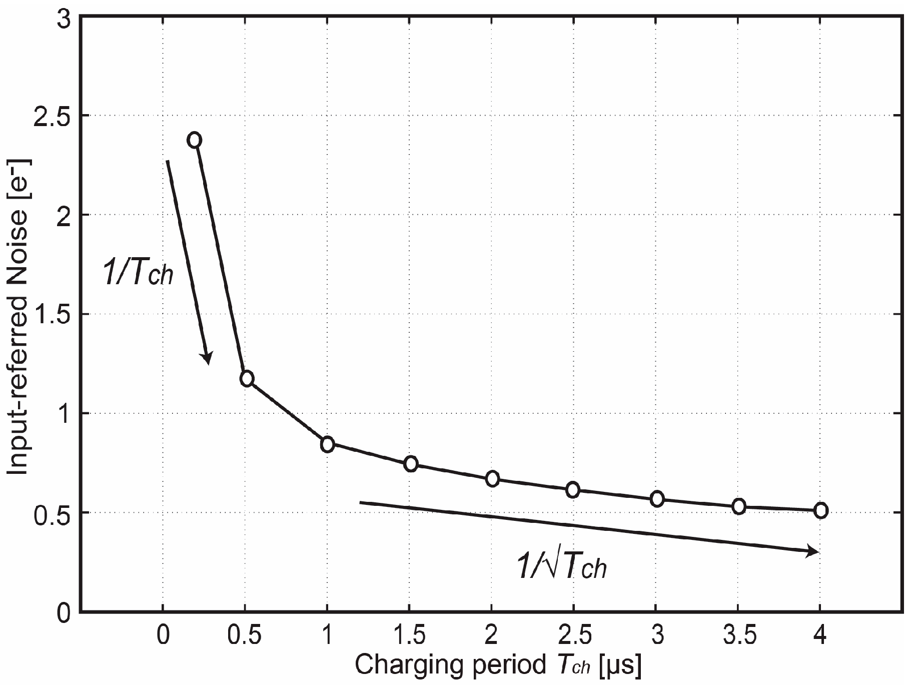
The temporal noise characterization has been done in the dark and implemented by keeping the transfer gate TG off during the measurement period. Figure 12 shows the measured input-referred noise of the proposed pixel as a function of Tch. The noise-reduction tendency initially is proportional to 1/Tch and later becomes proportional to 1/√Tch. This result indicates that the Gm-cell-based pixel not only reduces the noise originating from the exceeding circuits connected at the back of the pixel as a result of the signal amplification of the charge-sampling technique, but also suppresses the thermal noise generated by the pixel level circuit as a result of noise-bandwidth reduction. At Tch = 4 µs, the pixel achieves an input-referred noise of 0.51 e−rms. In addition, when referred the noise back to the input of the signal chain in the voltage domain by dividing its corresponding gain factor Apix, the lowest measured input-referred noise level is found around 27 µV, which is shown and compared with other state-of-the-art low-noise CIS in Figure 13. This figure presents that an improvement in figure-of-merit regarding the read-out noise reduction was successfully obtained by using the proposed Gm-cell-based pixel and charge-domain CDS technique.
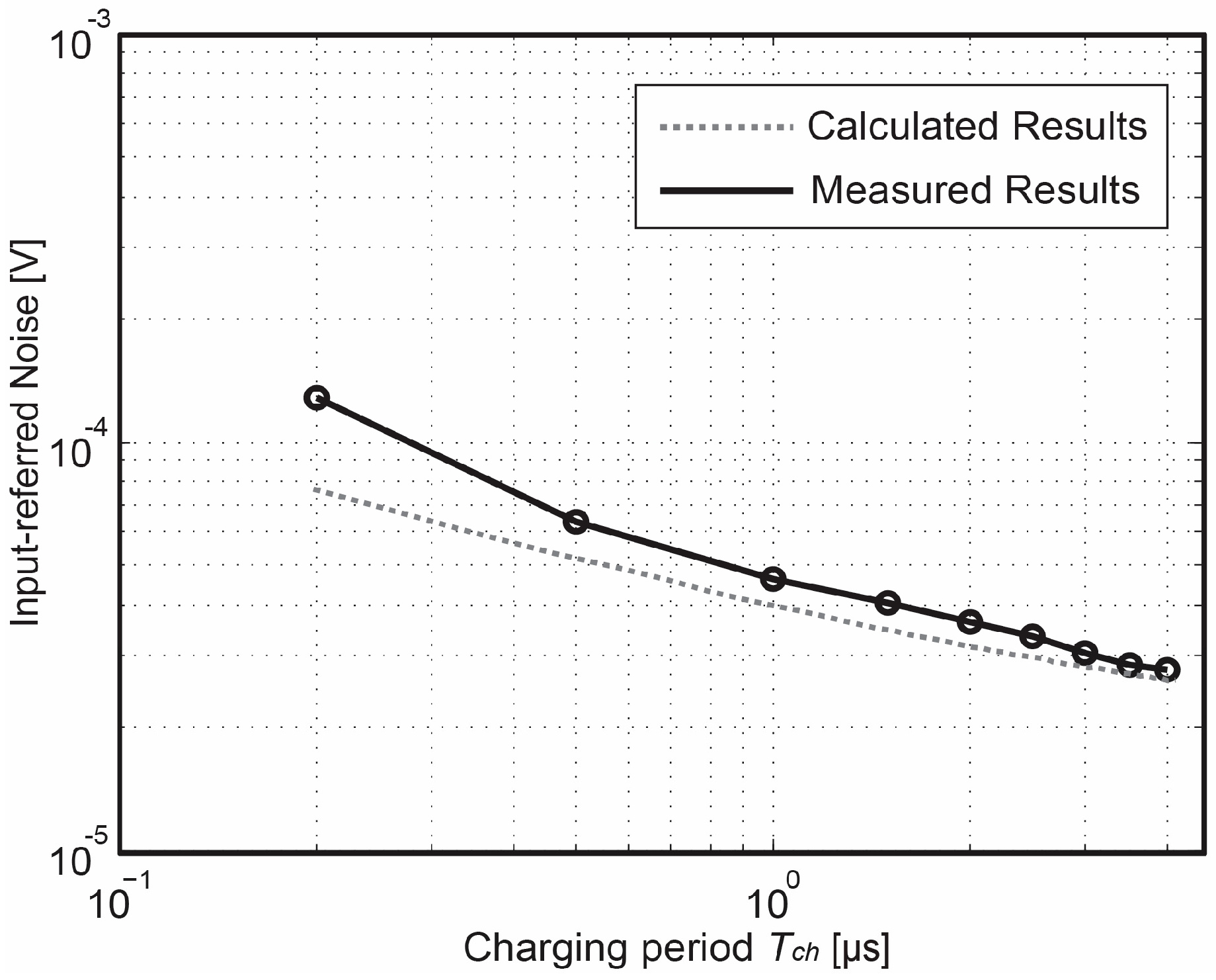
For verification of the time-domain noise analysis model, Figure 14 shows the measured input-referred noise with a comparison to the simulation results in voltage domain. In the calculation results described above, noise due to the clock jitter effect and sample and hold process, as well as the noise generated from the board-level succeeding readout circuits are ignored. As a result, there is a noise value deviation between the calculation and measurement results. Moreover, because of the trans-conductance is VFD-dependent and the Gm-cell is open loop, the gm variation degrades the pixel output linearity, leading to a noise reduction factor deviation between two results. As Figure 14 indicates, the noise reduction tendency obtained from the calculation model shows a steeper slope than the measurement results. However, the measured and calculated results show a reasonable agreement on the noise reduction tendency, demonstrating the validity of the noise calculation by using the time-domain noise analysis model.
5. Conclusions
A Gm-cell-based CMOS image sensor pixel structure that realizes a tunable conversion gain with a charge-domain CDS scheme was proposed for applications in low-noise high-DR image sensors. In contrast to conventional CIS pixel architectures, a Gm-cell-based pixel operates in a large-signal manner, and its noise behaves as a function of time. To allow a precise and predictive noise performance optimization for such type of pixels and their readout circuits, a non-stationery thermal and flicker noise analysis model based on a time-domain approach is presented and discussed in this paper. By comparing the numerical results derived from the proposed models with both simulation and experimental results, which showed a reasonable agreement, the effectiveness of the theoretical analysis model was verified.
Acknowledgments
The authors would like to thank TowerJazz for their support in silicon fabrication and the Dutch technology foundation STW for sponsoring the project.
Author Contributions
X.G. developed and designed the prototype CIS test chip; performed the characterization work and contributed to write this paper. A.T. contributed to the paper redaction, project conception, management and academic supervision.
Conflicts of Interest
The authors declare no conflict of interest.
References
- Lotto, C.; Seitz, P.; Baechler, T. A Sub-Electron Readout Noise CMOS Image Sensor with Pixel-Level Open-Loop Voltage Amplification. IEEE Int. Solid-State Circuits Conf. Dig. Tech. Papers 2011, 402–403. [Google Scholar] [CrossRef]
- Chen, Y.; Xu, Y.; Chae, Y.; Mierop, A.; Wang, X.; Theuwissen, A. A 0.7 e−rms Temporal-Readout-Noise CMOS Image Sensor for Low-Light-Level Imaging. In Proceedings of the 2012 IEEE International Solid-State Circuits Conference, San Francisco, CA, USA, 19–23 February 2012; pp. 384–385. [Google Scholar] [CrossRef]
- Yeh, S.-F.; Chou, K.-Y.; Tu, H.-Y.; Chao, C.Y.-P.; Hsueh, F.-L. A 0.66 e−rms Temporal-Readout-Noise 3D-Stacked CMOS Image Sensor with Conditional Correlated Multiple Sampling (CCMS) Technique. Proc. Symp. VLSI Circuits 2015, 53, 527–537. [Google Scholar] [CrossRef]
- Boukhayma, A.; Peizerat, A.; Enz, C. A Sub-0.5 Electron Read Noise VGA Image Sensor in a Standard CMOS Process. IEEE J. Solid-State Circuits 2016, 51, 2180–2191. [Google Scholar] [CrossRef]
- Boukhayma, A.; Peizerat, A.; Enz, C. Temporal readout noise analysis and reduction techniques for low-light CMOS image sensors. IEEE Trans. Electron Devices 2016, 63, 72–78. [Google Scholar] [CrossRef]
- Seo, M.-W.; Kawahito, S.; Kagawa, K.; Yasutomi, K. A 0.27 e−rms read noise 220 µV/e− conversion gain reset-gate-less CMOS image sensor with 0.11 µm CIS process. IEEE Electron Device Lett. 2015, 36, 1344–1347. [Google Scholar]
- Seo, M.-W.; Wang, T.; Jun, S.-W.; Akahori, T.; Kawahito, S. A 0.44 e−rms Read-Noise 32 fps 0.5 Mpixel High-Sensitivity RG-Less-Pixel CMOS Image Sensor Using Bootstrapping Reset. In Proceedings of the 2017 IEEE International Solid-State Circuits Conference (ISSCC), San Francisco, CA, USA, 5–9 February 2017; pp. 80–81. [Google Scholar] [CrossRef]
- Ma, J.; Fossum, E. Quanta Image Sensor Jot with Sub 0.3 e−rms Read Noise and Photon Counting Capability. IEEE Electron Device Lett 2015, 36, 926–928. [Google Scholar] [CrossRef]
- Ma, J.; Starkey, K.; Rao, A.; Odame, K.; Fossum, E. Characterization of Quanta Image Sensor Pump-Gate Jots with Deep Sub-electron Read Noise. IEEE J. Electron Devices Soc. 2015, 3, 472–480. [Google Scholar] [CrossRef]
- Wakashima, S.; Kusuhara, F.; Kuroda, R.; Sugawa, S. A linear response single exposure CMOS image sensor with 0.5 e− readout noise and 76 ke− full well capacity. In Proceedings of the 2015 Symposium on VLSI Circuits (VLSI Circuits), Kyoto, Japan, 17–19 June 2015; pp. C88–C89. [Google Scholar] [CrossRef]
- Yao, Q.; Dierickx, B.; Dupont, B.; Ruttens, G. CMOS image sensor reaching 0.34 e−rms read noise by inversion-accumulation cycling. In Proceedings of the International Image Sensor Workshop (IISW), Vaals, The Netherlands, 8–11 June 2015. [Google Scholar]
- Ge, X.; Theuwissen, A. A 0.5 e−rms Temporal-Noise CMOS Image Sensor with Charge-Domain CDS and Period-Controlled Variable Conversion Gain. In Proceedings of the International Image Sensor Society Workshop, Hiroshima, Japan, 30 May–2 June 2017; pp. 290–293. [Google Scholar]
- Ge, X.; Theuwissen, A. A 0.5 e−rms Temporal-Noise CMOS Image Sensor with Gm-Cell-Based Pixel and Period-Controlled Variable Conversion Gain. IEEE Trans. Electron Devices 2017, 64, 5019–5024. [Google Scholar] [CrossRef]
- Sepke, T.; Holloway, P.; Sodini, C.G.; Lee, H.-S. Noise analysis for comparator-based circuits. IEEE Trans. Circuits Syst. 2004, 56, 541–553. [Google Scholar] [CrossRef]
- Karvonen, S.; Riley, T.; Kurtti, S.; Kostamovaara, J. A quadrature chargedomain sampler with embedded FIR and IIR filtering functions. IEEE J. Solid-State Circuits 2006, 41, 507–515. [Google Scholar] [CrossRef]
- Mirzaei, A.; Chehrazi, S.; Bagheri, R.; Abidi, A. Analysis of first-order antialiasing integration sampler. IEEE Trans. Circuits Syst. I Regular Papers 2008, 55, 2994–3005. [Google Scholar] [CrossRef]
- Unser, M. Sampling-50 Years after Shannon. Proc. IEEE 2000, 88, 569–587. [Google Scholar] [CrossRef]
- Wey, H.; Guggenbuhl, W. Noise transfer characteristics of a correlated double sampling circuit. IEEE Trans. Circuits Syst. 1986, 29, 1028–1030. [Google Scholar] [CrossRef]
- Tohidian, M.; Madadi, I.; Staszewski, R.B. Analysis and design of a high-order discrete-time passive IIR low-pass filter. IEEE J. Solid-State Circuits 2014, 49, 2575–2587. [Google Scholar] [CrossRef]
- Martin-Gonthier, P.; Magnan, P. CMOS image sensor noise analysis through noise power spectral density including undersampling effect due to readout sequence. IEEE Trans. Electron Devices 2014, 61, 2834–2842. [Google Scholar] [CrossRef]
- Kawai, N.; Kawahito, S. Noise analysis of high-gain, low-noise column readout circuits for CMOS image sensors. IEEE Trans. Electron Devices 2004, 51, 185–194. [Google Scholar] [CrossRef]
- Papoulis, A. Probability, Random Variables, and Stochastic Process; McGraw-Hill, Inc.: New York, NY, USA, 1991; pp. 310–311. ISBN 0-07-048477-5. [Google Scholar]
- Terry, S.C.; Blalock, B.J.; Rochelle, J.M.; Ericson, M.N.; Caylor, S.D. Time-domain noise analysis of linear time-invariant and linear time-variant systems using MATLAB and HSPICE. IEEE Trans. Nuclear Sci. 2005, 52. [Google Scholar] [CrossRef]
- Chow, A.; Lee, H. Transient noise analysis for comparator-based switched-capacitor circuits. In Proceedings of the 2007 IEEE International Symposium on Circuits and Systems, New Orleans, LA, USA, 27–30 May 2007; pp. 953–956. [Google Scholar]
- Tian, H.; Gamal, A.E. Analysis of 1/f noise in CMOS APS. In Proceedings of the 2000 Electronic Imaging, San Jose, CA, USA, 15 May 2000; pp. 421–430. [Google Scholar] [CrossRef]
- Redeka, V. 1/f noise in physical measurements. IEEE Trans. Nuclear Sci. 1969, 16, 17–35. [Google Scholar] [CrossRef]
- Guo, W. Flicker noise process analysis. In Proceedings of the 1993 IEEE International Frequency Control Symposium, Salt Lake City, UT, USA, USA, 2–4 June 1993. [Google Scholar] [CrossRef]
- Ge, X.; Theuwissen, A. A CMOS image sensor with nearly unity-gain source follower and optimized column amplifier. In Proceedings of the 2016 IEEE SENSORS, Orlando, FL, USA, 30 October–3 November 2016. [Google Scholar] [CrossRef]
Figure 1.
Basic schematic (a) and timing diagram (b) of the Gm-cell-based pixel with charge-domain sampling.
Figure 1.
Basic schematic (a) and timing diagram (b) of the Gm-cell-based pixel with charge-domain sampling.
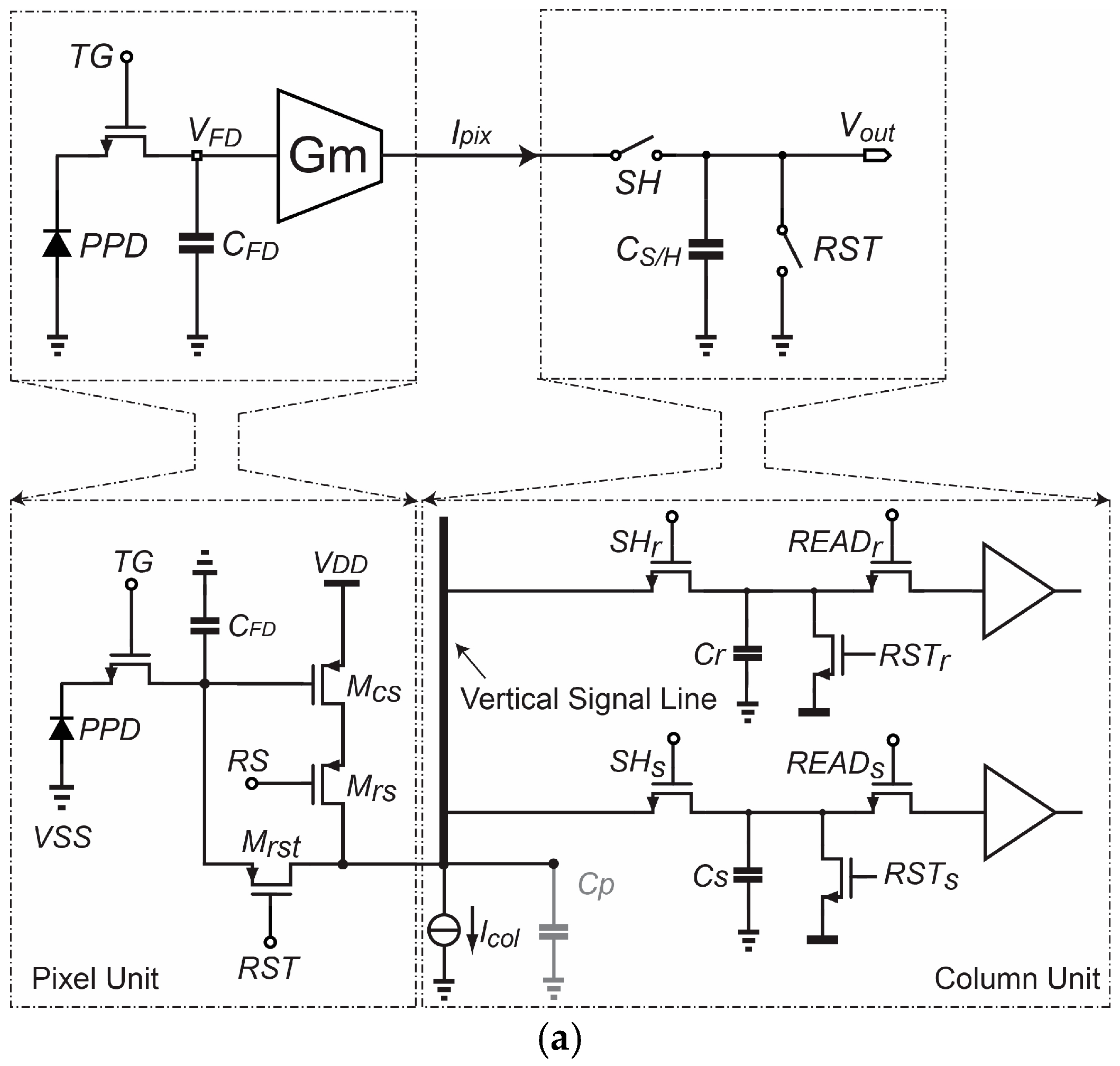
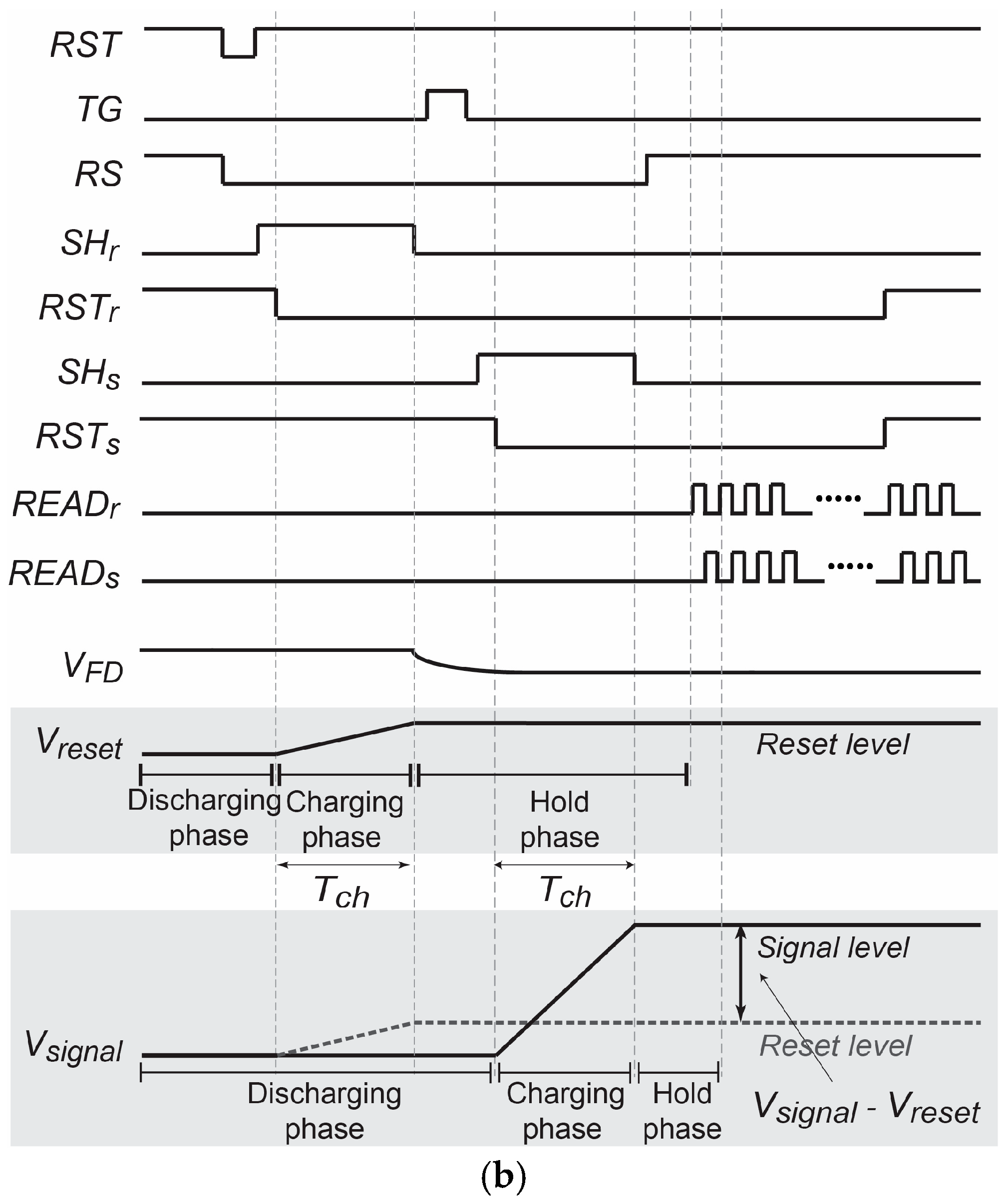
Figure 2.
Transfer functions of the charge-domain sampling vs. voltage-domain sampling. The overall roll-off of the transfer function of charge-domain is −40 dB, one −20 dB introduced by the zero-order hold (ZOH) effect by the discrete-time sampler, the additional −20 dB introduced by the charge-domain sampler.

Figure 3.
Block diagram model of the charge-domain correlated-double sampling (CDS).
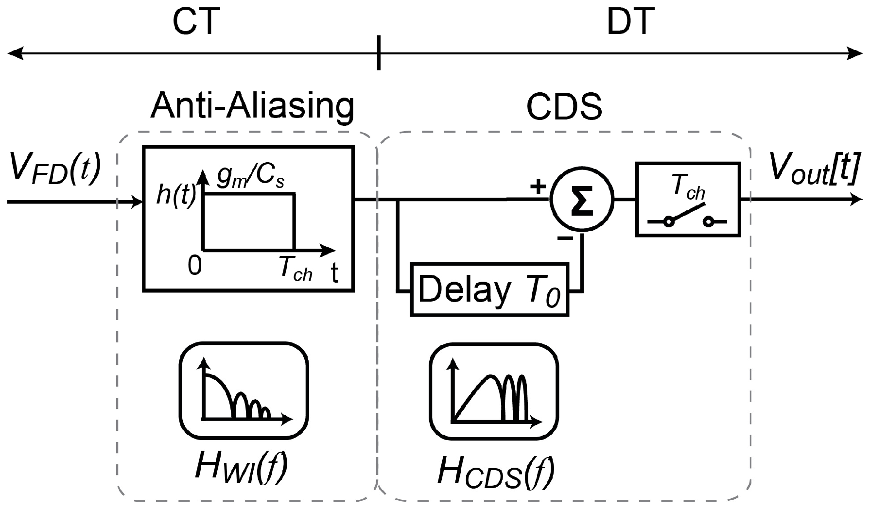
Figure 4.
Transfer function of the charge-domain CDS vs. voltage-domain CDS.
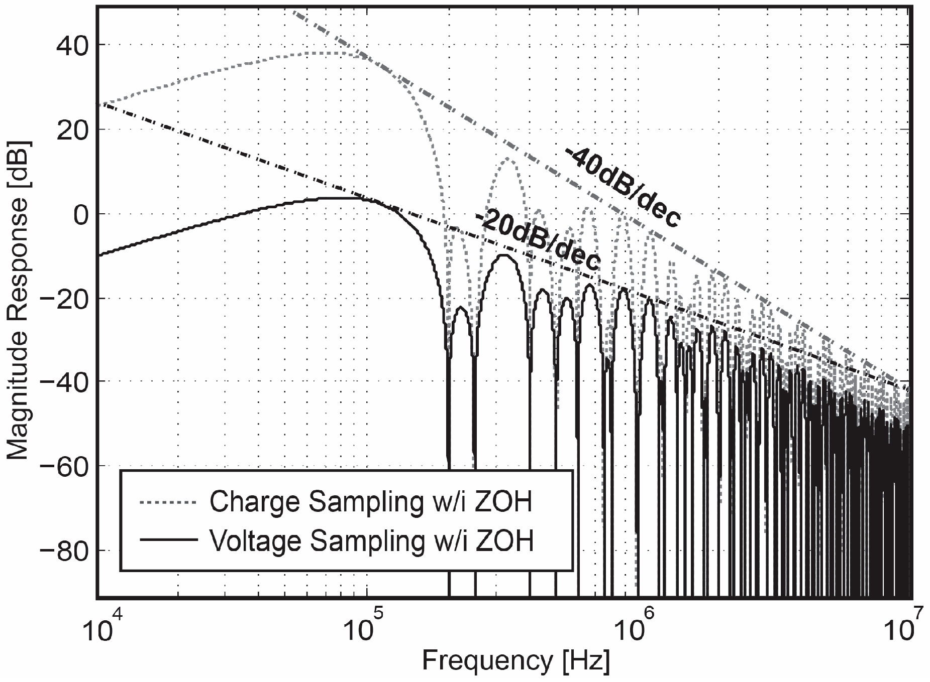
Figure 5.
(a) Steady-state noise waveform for source followers (SF)-based pixel (b) Non-steady-state noise waveform for Gm-cell-based pixel.
Figure 5.
(a) Steady-state noise waveform for source followers (SF)-based pixel (b) Non-steady-state noise waveform for Gm-cell-based pixel.
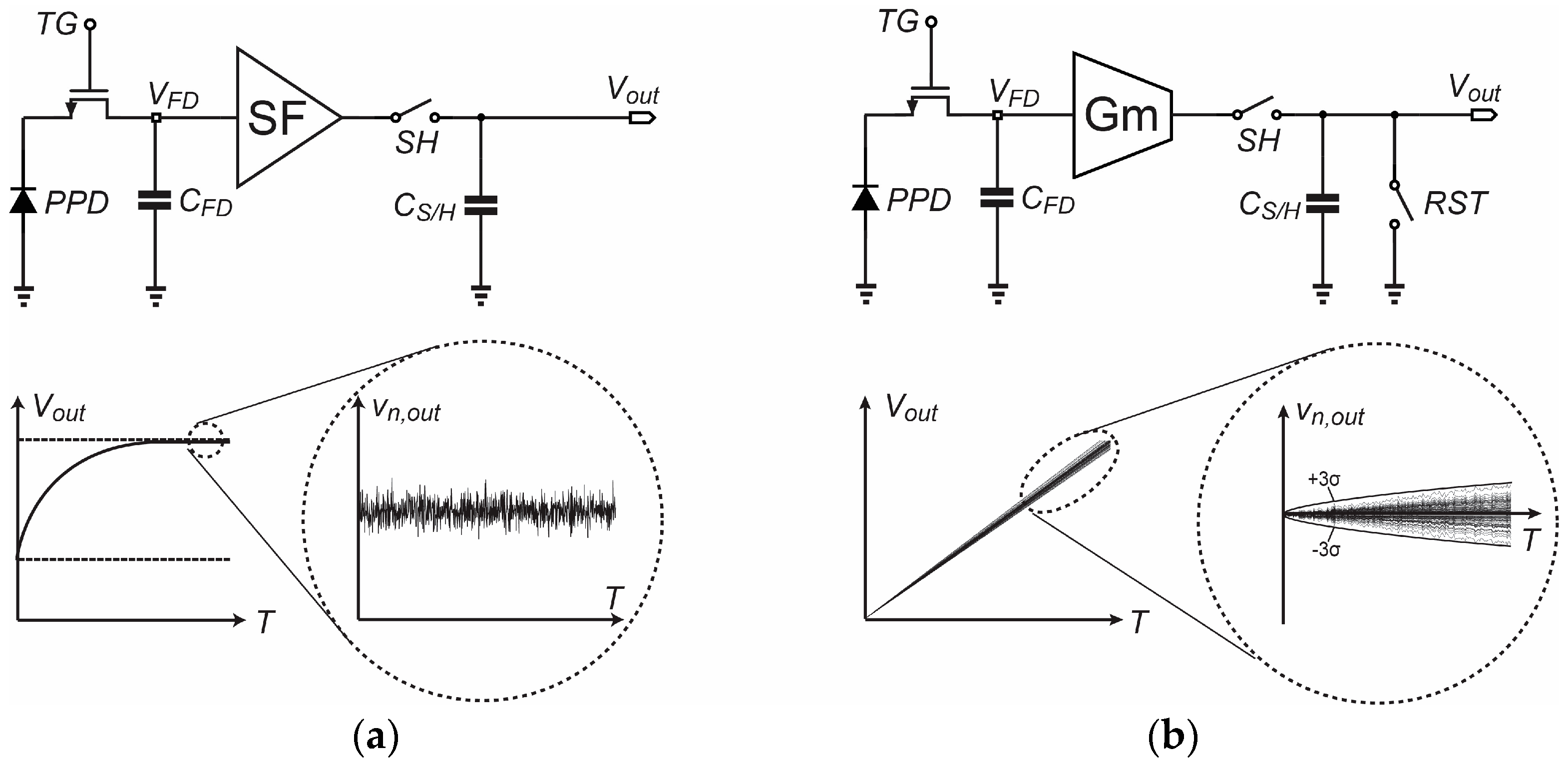
Figure 6.
(a) Noise model (b) Small signal model of Gm-cell-based pixel.

Figure 7.
Noise gain factor as a function of charging period Tch (a) with τ and ROUT increasing (b) with τ and CL increasing.
Figure 7.
Noise gain factor as a function of charging period Tch (a) with τ and ROUT increasing (b) with τ and CL increasing.

Figure 8.
Input referred thermal noise as a function of charging period Tch.
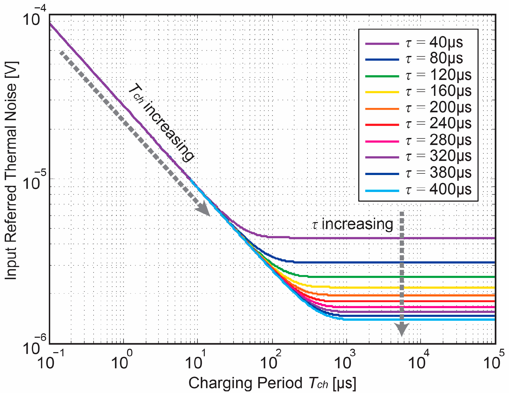
Figure 9.
Input referred flicker noise as a function of charging period Tch.
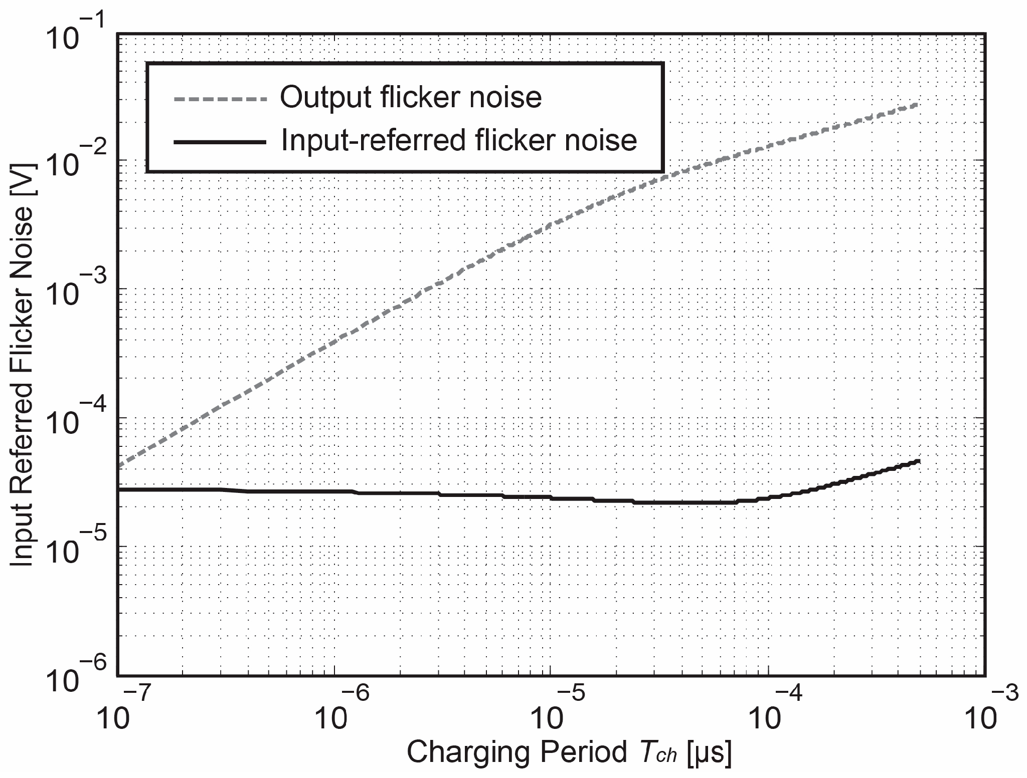
Figure 10.
Input referred kTC noise as a function of charging period Tch during discharging phase (a) with τ and CL increasing (b) with τ and ROUT increasing.
Figure 10.
Input referred kTC noise as a function of charging period Tch during discharging phase (a) with τ and CL increasing (b) with τ and ROUT increasing.
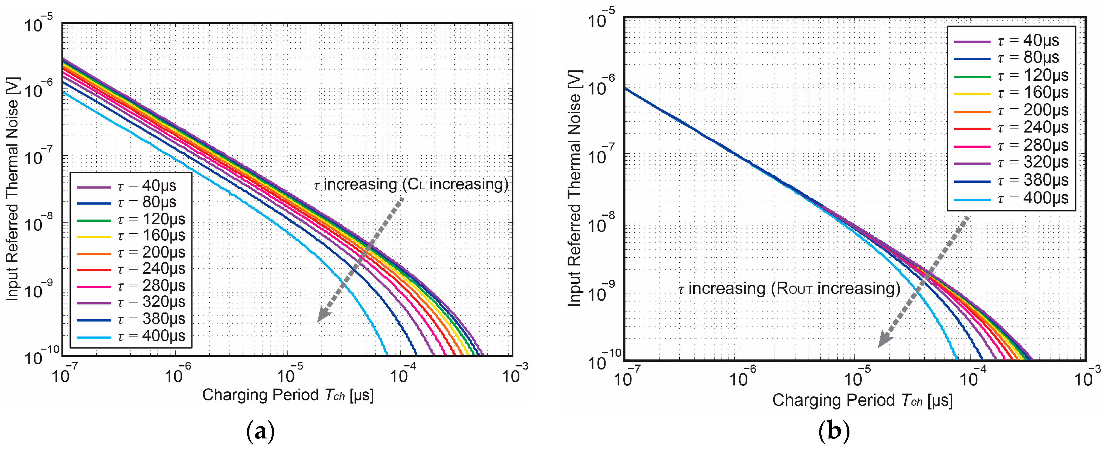
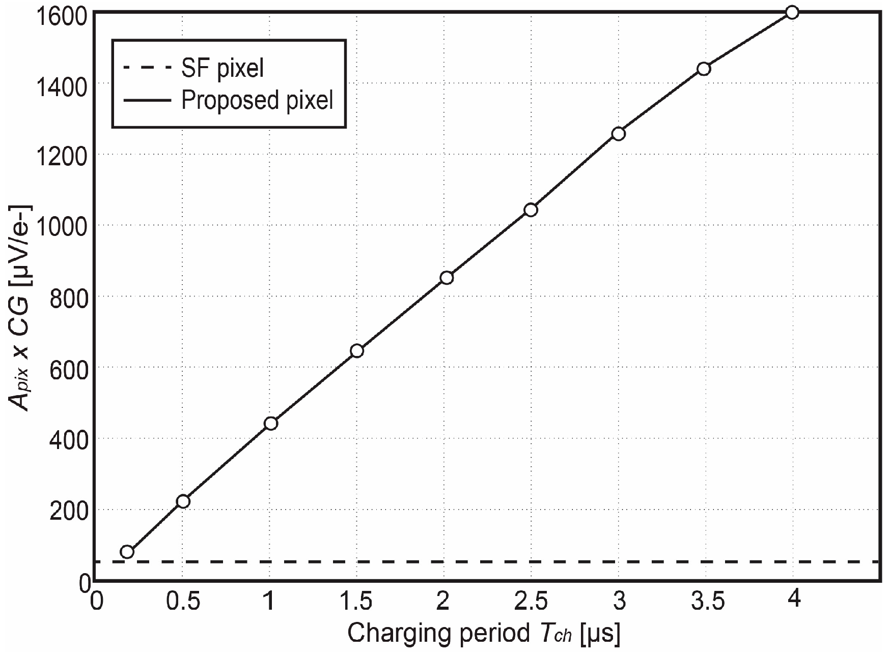
Figure 12.
Measured input-referred noise as a function of the charging period Tch [12].
Figure 12.
Measured input-referred noise as a function of the charging period Tch [12].

Figure 13.
Comparison of input-referred noise in the electron domain vs. FD capacitance, and noise trend in the voltage domain with reported image sensors. The values are based on the best guess with the known values of CGFD in reported publications [13].
Figure 13.
Comparison of input-referred noise in the electron domain vs. FD capacitance, and noise trend in the voltage domain with reported image sensors. The values are based on the best guess with the known values of CGFD in reported publications [13].
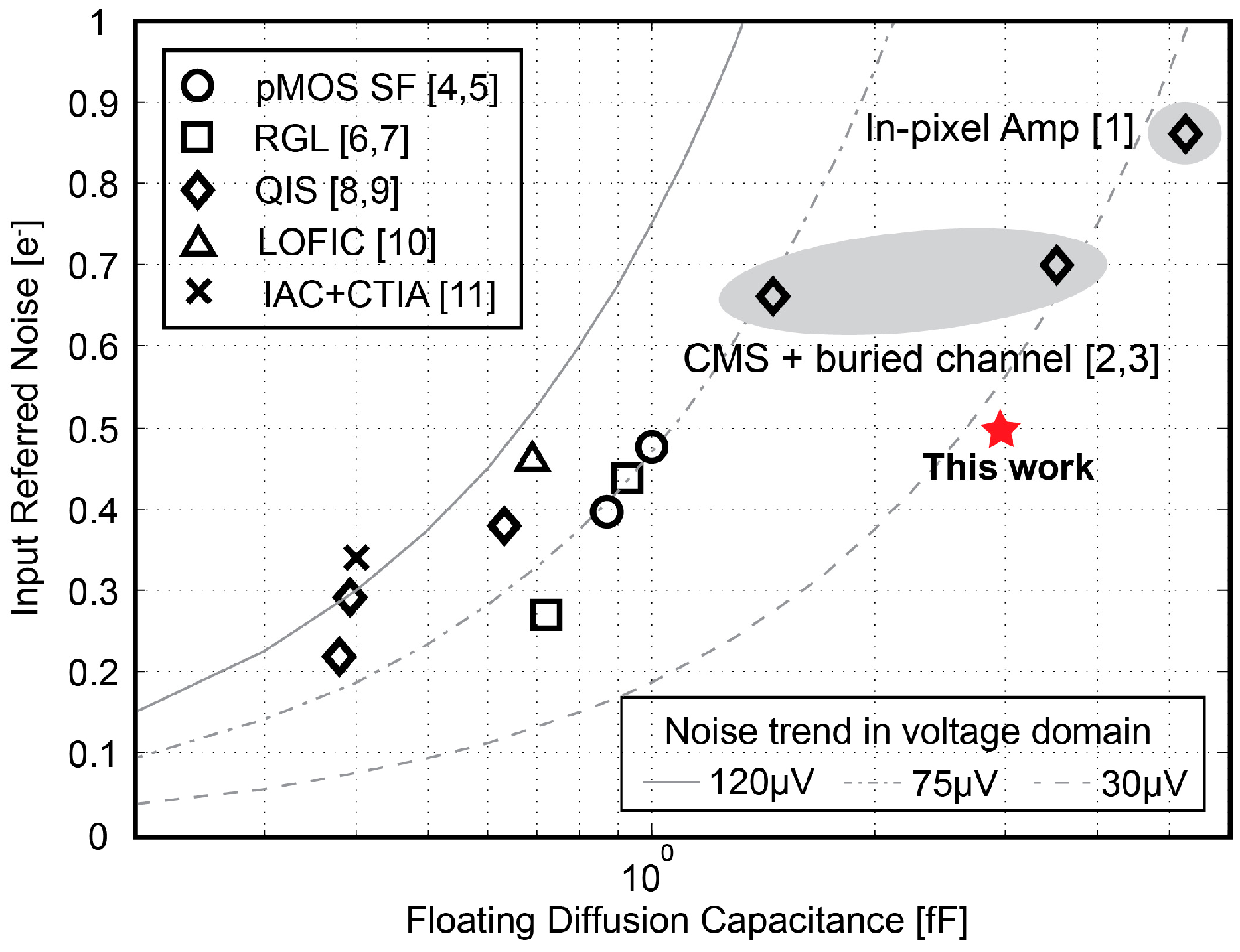
Figure 14.
Input-referred noise in voltage domain as a function of Tch for measured and simulated results.
Figure 14.
Input-referred noise in voltage domain as a function of Tch for measured and simulated results.


Table 1.
Device parameter used for the noise estimation.
| Parameter | Value | Parameter | Value |
|---|---|---|---|
| gm1 | 30 µS | A | 3 µm (W) × 0.5 µm (L) |
| Cp | 2 pF | K | 1 × 10⁻²⁵ |
| Ro,Gm | 20 MΩ | Cox | 4.3 fF/µm2 |
| k | 1.38 × 10⁻²³ | fc | 500 kHz |
| T | 300 K | top | ~1 h |
© 2018 by the authors. Licensee MDPI, Basel, Switzerland. This article is an open access article distributed under the terms and conditions of the Creative Commons Attribution (CC BY) license (http://creativecommons.org/licenses/by/4.0/).
Share and Cite
MDPI and ACS Style
Ge, X.; Theuwissen, A.J.P. Temporal Noise Analysis of Charge-Domain Sampling Readout Circuits for CMOS Image Sensors. Sensors 2018, 18, 707. https://doi.org/10.3390/s18030707
AMA Style
Ge X, Theuwissen AJP. Temporal Noise Analysis of Charge-Domain Sampling Readout Circuits for CMOS Image Sensors. Sensors. 2018; 18(3):707. https://doi.org/10.3390/s18030707
Chicago/Turabian StyleGe, Xiaoliang, and Albert J. P. Theuwissen. 2018. "Temporal Noise Analysis of Charge-Domain Sampling Readout Circuits for CMOS Image Sensors" Sensors 18, no. 3: 707. https://doi.org/10.3390/s18030707
Note that from the first issue of 2016, this journal uses article numbers instead of page numbers. See further details here.