1. Introduction
Electric field measurement is essential in many scientific and industrial fields, such as power system monitoring [
1,
2], meteorological phenomena studies [
3,
4], and electrostatic protection [
5,
6], etc. Responding to different measurement environments (e.g., temperature and state of matter) and different characteristics of the measured electric field (e.g., frequency, amplitude, duration and direction) in these applications, plenty of principles and techniques have been applied in electric field measurement, and a variety of electric field sensors (EFSs) have been developed. In the last two decades, with the rapid development of Micro-electro-mechanical Systems (MEMS) technology, much literature on electric field sensor chips (EFSCs) has emerged, providing various EFSCs with the advantages of low power cost, small size, high integration, and convenience for batch production. These EFSCs can be classified into three categories according to their working principles, namely, induction charge [
7,
8,
9,
10,
11,
12], electrostatic force [
13,
14], and steered-electrons [
15]. These EFSCs focus on direct current (DC) and low-frequency alternating current (AC) electric field measurement. The most reported EFSCs are single-axis ones, whose sensing axes are perpendicular to their upper surfaces. However, in many cases (e.g., in high voltage infrastructure [
1] and atmospheric studies [
16,
17]) the electric field has an unknown direction before measurement. Thus, sensors that can accurately detect and quantify three-dimensional (3D) electric fields in natural and artificial environments are in demand.
A typical 3D EFS consists of three orthogonal sensing axes to sense three Cartesian components of the electric field simultaneously. One of the major concerns in developing 3D EFS is its susceptibility to cross-axis coupling interference. In other words, the output signal for each sensing axis of the 3D EFS is often coupled with electric field components from the two other orthogonal sensing axes. For example, the output signal for the
X-axis of a 3D EFS is probably coupled with electric field components from the
Y- and
Z-axes, affecting the accuracy of 3D electric field measurement. Its performance index is cross-axis sensitivity expressed as the ratio of the measured sensitivity in the cross-direction to the measured sensitivity in the sensing direction, which is widely employed in evaluating 3D sensors, including 3D accelerometers [
18].
Aimed at developing MEMS-based 3D EFSs with low cross-axis coupling interference, some relevant works have been reported concerning algorithms and novel micromachined sensor structures. Wen [
19] firstly derived a 3 × 3 coupling sensitivity matrix with pre-measured cross-axis sensitivities, and employed this matrix to compensate the measurement results from three typical one-dimensional (1D) EFSCs. Li [
20] introduced a genetic algorithm (GA) to determine the coupling sensitivity matrix. Although their methods can be easily implemented and are minimally restrictive, their studies merely rely on the algorithm rather than sensor structure and are incapable of eliminating cross-axis coupling interference at the source. Higher cross-axis coupling interference means higher cross-axis sensitivity in that matrix, and consequently leads to larger 3D electric field measurement errors. Ling [
21] investigated cross-axis coupling interference elimination in terms of symmetrical structures combined with a difference circuit. He firstly presented a single-chip 3D EFSC, where two pairs of sensing elements are located symmetrically to form a cross-like shape with each pair to obtain the
X- and
Y-axis electric field components, respectively. Sensing elements in each pair are designed to be identical in structure, so that cross-axis coupling interference on the
X and
Y sensing axes can be eliminated theoretically with a difference circuit. However, a symmetrically-located sensing structure is not available for the
Z-axes sensing element. Moreover, this device suffers from large driving voltage and low sensitivity owing to its great integrity and complicated sensor structure.
For the sake of accurate 3D electric field measurement, a MEMS-based 3D EFS with low cross-axis coupling interference is developed in this paper. The 3D EFS is composed of three identical 1D EFSCs forming three orthogonal sensing axes. In contrast to previously reported 1D EFSCs designed for perpendicular electric field component measurement, the proposed 1D EFSC is designed to be symmetrical, forming a pair of in-plane symmetrically-located sensing structures, which makes the 1D EFSC capable of sensing parallel electric field along symmetrical structures and eliminating cross-axis coupling interference. Moreover, the testing system and calibration system of the proposed 3D EFS are developed.
2. Structure Design and Working Principle
The 1D EFSC is designed to be symmetrical, as shown in
Figure 1a, and is fabricated on a silicon-on-insulator (SOI) die, as described in
Section 4. It is constructed from a resonator that is laterally actuated by push–pull comb drives. Strip-type electrodes are employed as sensing electrodes and shielding electrodes. Two arrays of fixed sensing electrodes are symmetrically placed and interdigitally coupled to their coplanar shielding electrodes. Two identical folded beams are arranged adjacent to push–pull comb drives and connected to shielding electrodes, with other ends anchored to ground, forming a movable shutter. The folded beam works as the elastic structure for the resonator since it can provide a much larger linear deflection range. The 1D EFSC is based on charge induction to sense the external electric field. Yang [
11] once presented the operational principle of the lateral EFSC in detail. When the movable shutter is laterally excited by push–pull comb drives, the shielding electrodes oscillate along axis of symmetry, covering the sidewalls of sensing electrodes periodically, as shown in
Figure 1b. As a result, the strength of electric field on the strip-type sensing electrodes varies periodically in the external electric field, and the alternating current is consequently induced. Notably, this external electric field can be either perpendicular to the chip or not. Sensing electrodes cause the distortion of the nearby electric field, so that an electric field can be generated on sensing electrodes even with a parallel external electric field. This is explained in detail in [
21].
In contrast to typical 1D EFSCs designed for sensing electric field components perpendicular to the chip, the proposed 1D EFSC focuses on sensing parallel electric field along symmetrical structures. The 1D EFSC is assumed to be placed on the
X-
Y plane with its sensing axis parallel to the
X-axis, and its axis of symmetry located on
Y-
Z plane and parallel with the
Y-axis, as shown in
Figure 1b. A uniform electric field is applied. For the
X-axis electric field component, the
Y-
Z plane is an equipotential plane as the 1D EFSC is symmetrical in structure. Thus, it can be inferred that the electric flux on the surfaces on these two sensing arrays are opposite theoretically, so that the induced charges on two arrays of sensing electrodes by
X-axis electric field component are opposite as well. However, the induced charges on two arrays of sensing electrodes by the
Y- and
Z-axis electric field components are identical. The outputs of two arrays of electrodes are connected to a difference circuit consisting of two identical I-V convertors and an instrumentation amplifier, which can eliminate the influences of electric field components along
Y- and
Z-axes, and leave the
X-axis electric field component alone. Detailed difference circuit information is presented in [
22]. Therefore, it can be inferred that each 1D EFSC is merely sensitive to electric field component along its sensing axis after the difference circuit.
Moreover, for gaining large vibration amplitude with low excitation voltage, each 1D EFSC works at its resonant frequency. A modal simulation of the movable shutter structure was conducted to predict its resonant frequencies and its corresponding vibration modes. Using the finite element analysis (FEA) method, the frequencies of the first five orders resonant modes were calculated to be 2552 Hz, 3496 Hz, 3532 Hz, 4684 Hz, and 7433 Hz respectively, in which the resonant frequency of lateral vibration mode was 2552 Hz. The key parameters of the proposed 1D EFSC are listed in
Table 1. The size of 1D EFSC is 6.4 mm × 6.4 mm.
3. Modeling of the 1D EFSC
Modeling analysis was performed to validate the capability of the proposed 1D EFSC in sensing parallel electric field along symmetrical structures and eliminating cross-axis coupling interference. The simulation model is illustrated
Figure 2, in which the 1D EFSC was simplified based on its outlines. Two arrays of electrodes were simplified into two rectangular sensing areas. The serpentine springs and push–pull comb drives were disregarded. Notably, these two rectangular sensing areas are electrically isolated, but the upper surface of this model is equipotential due to its testing circuit. The 1D EFSC was placed on the
X-
Y plane with the
Y-axis working as its axis of symmetry, so that its sensing axis was along the
X-axis. A uniform electric field with strength of
E1 was applied. The angle between the electric field and the
Z-axis was
θ. The angle between the projection of the electric field on the
X-
Y plane and
X-axis was
φ. Therefore,
where
Ex,
Ey, and
Ez are the
X-,
Y-, and
Z-axis components of the external electric field, respectively.
QA1 and
QA2 are the induced charges on sensing area I and sensing area II, respectively.
where
Qx is the differential output of these two sensing areas. Theoretically, the characteristics of
Qx with respect to
θ and
φ should be in accordance with
Ex, and have no relationship with
Ey and
Ez.
The FEA method was employed to simulate the induced charge on these two sensing areas with different external electric field directions. The boundary conditions for this simulation strictly follow those of calibration. Firstly, a cubic free space with sufficiently large dimensions was created, in which the simplified 1D EFSC was arranged at its center. Two opposite sides of this cubic free space were selected to apply opposite voltages for generating a uniform electric field. Thus, an electric field from different directions with respect to the 1D EFSC was generated by rotating the rectangular free space around its center, while the simplified 1D EFSC was kept still. E1 was set to be 10 V/m. Qx was calculated when the direction of the applied electric field changed circumferentially.
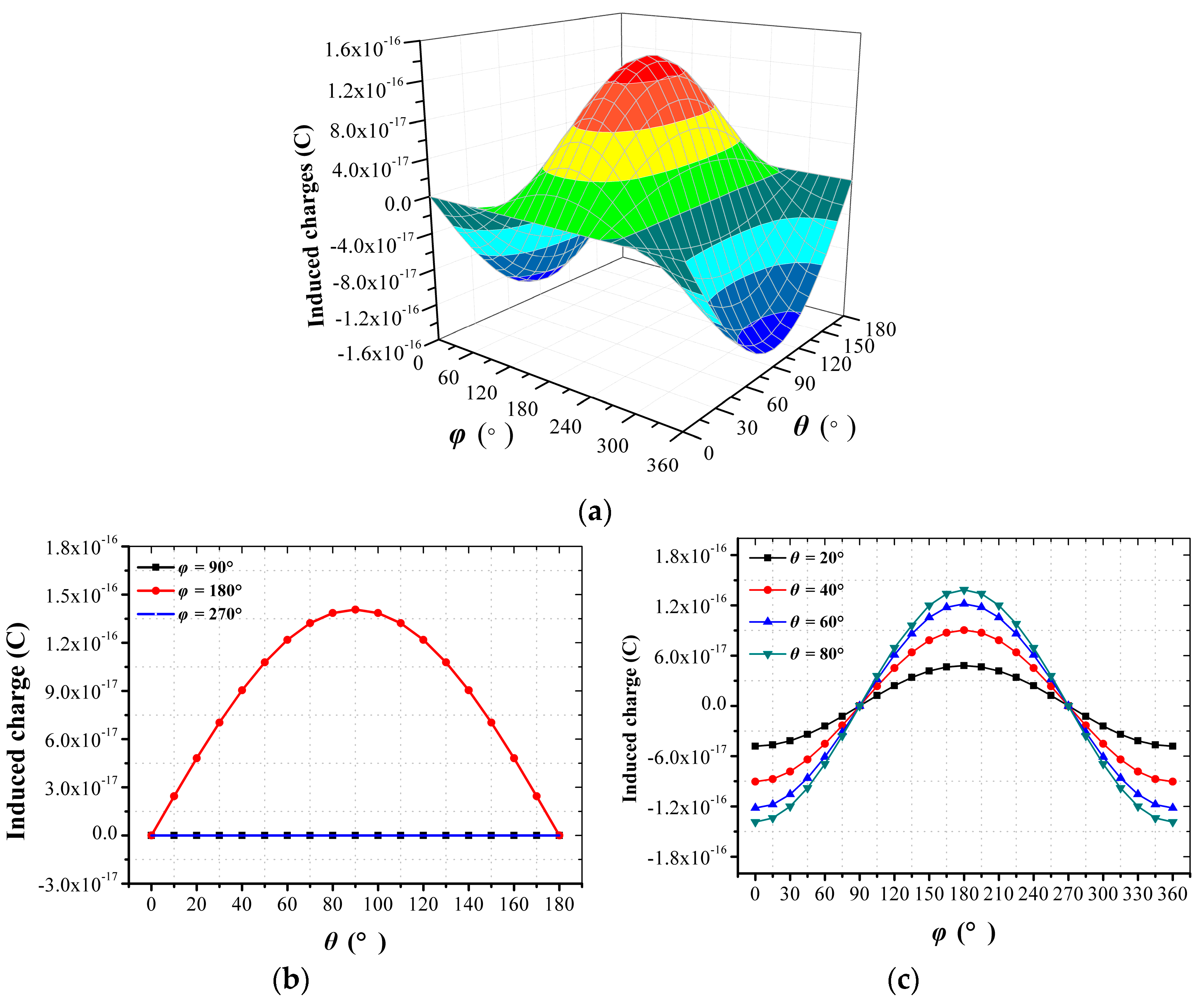
The relationship between
Qx and different combinations of
θ and
φ are presented in
Figure 3a. Then, some sections were taken from the 3D plot to illustrate this relationship better. As shown in
Figure 3b, when
φ was 0°, the curves about
Qx versus
θ showed good sinusoidal characteristics, whereas
Qx was zero when
φ was 90° and 270°. It can be inferred that
Qx is merely sensitive to
Ex, and has no relationship with
Ey and
Ez. As shown in
Figure 3c, when
θ was 20°, 40°, 60° and 80°, the curves with respect to
Qx versus
φ showed good sinusoidal characteristics. This illustrates that the characteristics of
Qx with respect to
θ and
φ were in good accordance with
Ex. The simulation results matched the previous assertion that the characteristics of
Qx with respect to
θ and
φ should be in accordance with
Ex, and have no relationship with
Ey and
Ez. Therefore, simulation results prove that the proposed 1D EFSC is capable of measuring electric field component along its sensing axis accurately without cross-axis coupling interference.
5. Assembly and Modeling of 3D EFS
Figure 6 illustrates the 3D EFS. Each 1D EFSC is stuck to an aluminum cuboid placed at the center of a printed circuit board (PCB). The cuboid is utilized to magnify the electric field distortion on chip, so as to improve the sensitivity of each 1D EFSC. Each PCB contained two identical I-V converters and an instrumentation amplifier in order to amplify the output of 1D EFSC locally. Its schematic view is shown in
Figure 1. By arranging these three PCBs forming three orthogonal sensing axes, a 3D EFS with low cross-axis coupling interference was realized.
Modeling analysis was performed to investigate the developed 3D EFS’s responses to 3D electric fields. The 3D EFS was simplified based on its outlines as well. The simplified simulation model was a combination of three orthogonally arranged plates, as shown in
Figure 7. The 1D EFSC was simplified into two rectangular sensing areas, similar to that of
Section 3, and arranged at the center of each plate. Electric field with strength of
E2 was applied. The angle between the electric field and
Z-axis was
α. The angle between the projection of the electric field on the
X-
Y plane and
X-axis was
β. The FEA method was used to calculate the induced charge on each 1D EFSC with respect to
α and
β. Notably, the FEA modeling work was similar to that in
Section 3.
As shown in
Figure 8a, when
α was 90°, the curves with respect to the induced charge on the
X- and
Y-axis 1D EFSCs showed good sinusoidal characteristics with a 90° phase difference, whereas the induced charge on
Z-axis 1D EFSC was almost zero. As shown in
Figure 8b, when
β was zero, the curves with respect to induced charge on the
X- and
Z-axis 1D EFSCs showed good sinusoidal characteristics, with a 90° phase difference, whereas induced charge on the
Y-axis 1D EFSC was almost zero. These curves were basically in good accordance with the electric field component on the
X-,
Y- and
Z-axes, but there exist residual cross-axis sensitivities, especially in
Figure 8a. The sensitivity of the
Z-axis 1D EFSC to the
Y-axis electric field components is non-zero, and the cross-axis sensitivities were calculated to be within 1.45%. The simulation model is a combination of three plates rather than cuboid, so that dissymmetry is introduced into this model. Ideally, the cross-axis sensitivities are zero if the proposed 3D EFS is cube-shaped. Therefore, simulation results prove that the proposed 3D EFS is capable of eliminating cross-axis coupling interference effectively but its dissymmetry makes it fail to eliminate cross-axis coupling interference thoroughly.
6. Characterization
6.1. Testing and Calibration Systems
To measure the outputs of three 1D EFSCs simultaneously, this paper for the first time developed a miniaturized testing system. Considering that these three 1D EFSCs are independent of each other, the testing system can be divided into three sensing channels. Each sensing channel includes a driving signal generator, I-V converter, instrumentation amplifier, band-pass filter, multiplier, and low-pass filter. Among them, the I-V converter and instrumentation amplifier work as a front-end amplification system, as shown in
Figure 1 and
Figure 6. The rest form the back-end processing system whose job is to generate driving signals, sample and process the outputs from the front-end amplification system, and upload the measured results. The schematic view is shown in
Figure 9.
For each sensing channel, a pair of driving signals, each composed of 20 V DC bias voltage and 1 V AC voltage, are generated to excite the 1D EFSC. Notably, to push–pull the movable structure of the 1D EFSC, these two driving signals are identical but have a 180° phase difference in their AC voltage. Furthermore, to gain a large vibration amplitude, the frequency of AC voltage is close to the resonant frequency of 1D EFSC. The resonant frequencies of these three 1D EFSCs were detected to be 2220 Hz, 2220 Hz, and 2250 Hz, respectively, after the frequency sweep. The simplified structure for modal simulation, error of chip fabrication, and air damping account for the difference between the simulated resonant frequencies and detected resonant frequencies. Multiplier and low-pass filters are created digitally in the MCU. They work as a lock-in amplifier to extract the amplitude of the sensing signal, which is proportional to the applied electric field strength.
Figure 10 illustrates the calibration system. Two parallel metal plates were applied with opposite voltages respectively to generate a uniform electric field. Equally spaced iron wires, along with equivalent resistances electrically connecting the adjacent two iron wires as well as a metal plate and the adjacent iron wire, were employed to minimize the fringe effect of two parallel metal plates. These two parallel metal plates and iron wires formed a cubic uniform electric field space. The 3D EFS was fixed to one end of a Teflon rod, and arranged at the center of the uniform electric field space. The Teflon rod was parallel with two metal plates. The rod had two orthogonal and intersecting rotation axes, R1 and R2, and its intersection was coincident with the center of the 3D EFS, which caused the center of the 3D EFS to stay still in rotation. Notably, the other end of the rod was connected with a rotary motor, so that the rotation around R1 could be electrically controlled, while the rotation around R2 was manually controlled.
6.2. Calibration
By rotating the 3D EFS around rotation axes R1 and R2, electric fields parallel with the
X-,
Y- and
Z-axes of the respective 3D EFSs were applied. In each case, the outputs of the
X-,
Y- and
Z-axis 1D EFSCs with respect to the electric field strength ranging from 0 to 120 kV/m were all recorded for calibration, as shown in
Figure 11.
The sensitivities of the
X-,
Y- and
Z-axis 1D EFSCs in the three cases are listed in
Table 2. It is obvious that the cross-axis sensitivities are within 5.48%. Besides the inherent cross-axis sensitivity described in
Section 5, the error induced by assembly and chip fabrication may account for the rest of the cross-axis sensitivity. However, these errors can be estimated and minimized with strict and high standards of chip fabrication and 3D assembly. All the measured linearity errors for these three 1D EFSCs were within 1.8%, which revealed that each 1D EFSC had good linearity.
A comparison of cross-axis sensitivities of the recently reported MEMS-based 3D EFSs was conducted, and the results are listed in
Table 3, showing that the cross-axis coupling interference was eliminated effectively in this paper. Furthermore, each 1D EFSC of this 3D EFS was tested in the three roundtrip measurements with the electric field along its sensing axes. In the range of 0–120 kV/m, the uncertainties of these three 1D EFSCs were calculated to be within 1.92%, which revealed that the 3D EFS was insusceptible to noise.
The coupling characteristics can be expressed by the following matrix.
where
Vq is the output voltage of the
q-axis 1D EFSC,
Vq0 is the zero output voltage of the
q-axis 1D EFSC, and coupling sensitivity
kqi is the sensitivity of the
q-axis 1D EFSC to the electric field in the direction
i;
i =
x,
y,
z, and
q =
x,
y,
z. Therefore, the electric field can be expressed as
Thus, in this study, the coupling matrix is given by
6.3. 3D Electric Field Measurement and Verification
Experiments were conducted to investigate the measurement accuracy of the developed 3D EFS. The 3D EFS was rotated to several random angles (θ1, θ2, θ3, θ4, and θ5). For each angle, electric fields of 50 and 100 kV/m were respectively applied, so that the direction of applied electric field was random. The outputs of the X-, Y-, and Z-axes 1D EFSCs were recorded, and Ex, Ey, and Ez were derived afterwards. The strength of the applied electric field was computed with
The comparison between the applied and calculated electric fields is listed in
Table 4. The measurement errors were of less than 6.16%. Thus, it can be concluded that the calculated electric field of the 3D EFS was basically consistent with the applied electric field, but measurement errors still existed. Systematic errors, assembly-induced errors, and fabrication-induced dissymmetry of 1D EFSC may account for the measurement errors. Likewise, these errors can be minimized with appropriate noise shielding in the testing circuit, and high standards of chip fabrication and 3D assembly.

 ,
, 


