Ultraviolet Detectors Based on Wide Bandgap Semiconductor Nanowire: A Review

Abstract
:1. Introduction
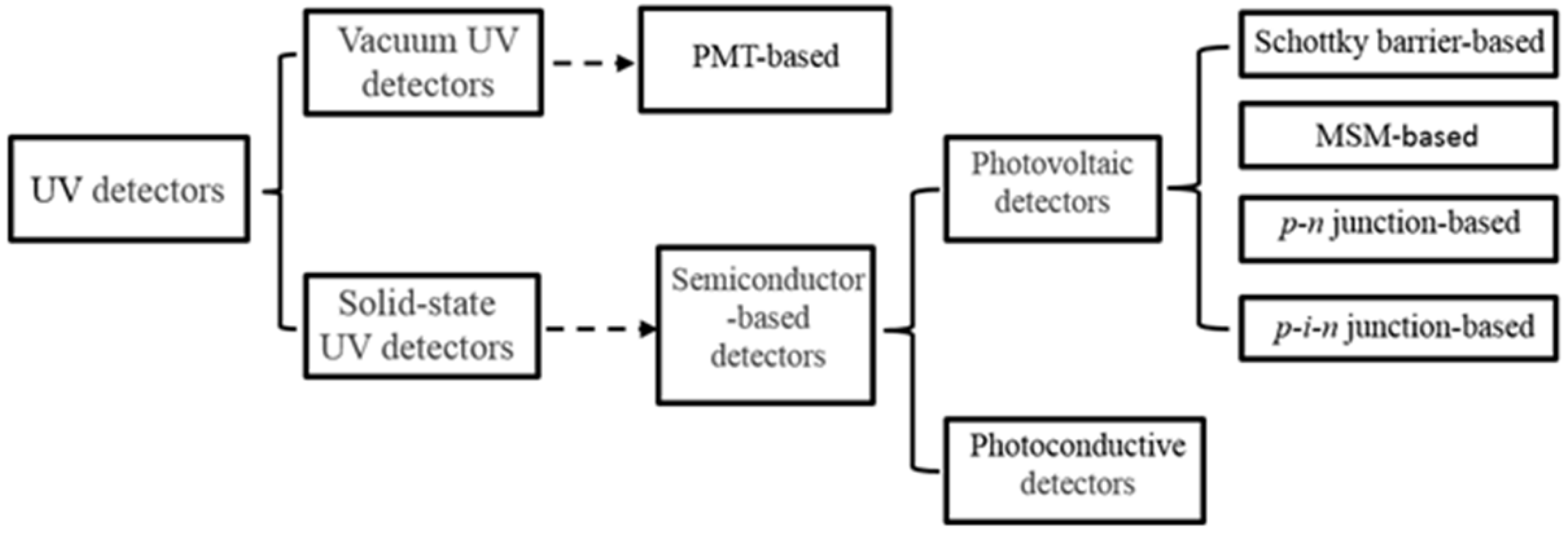
2. UV Detectors
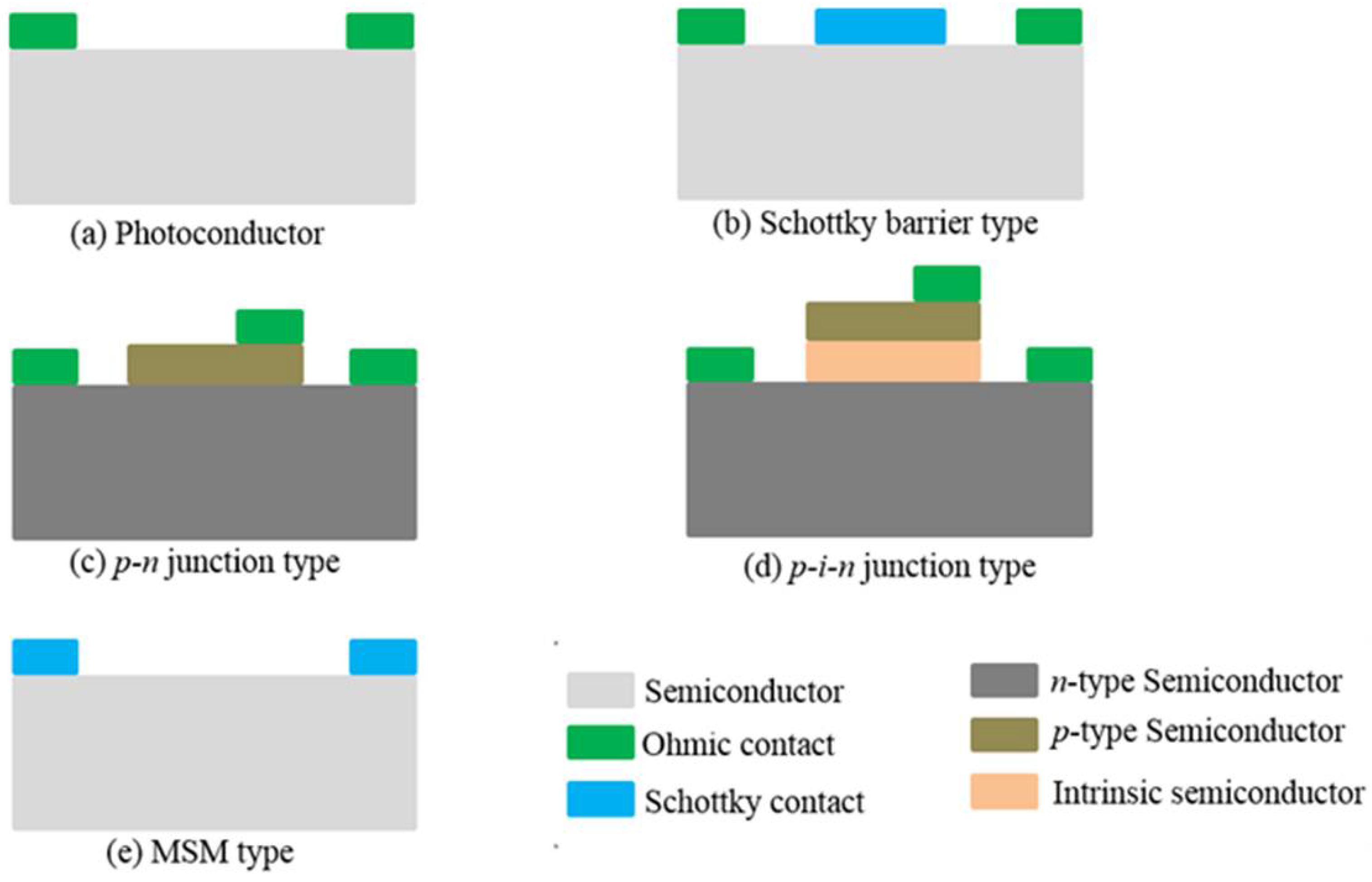
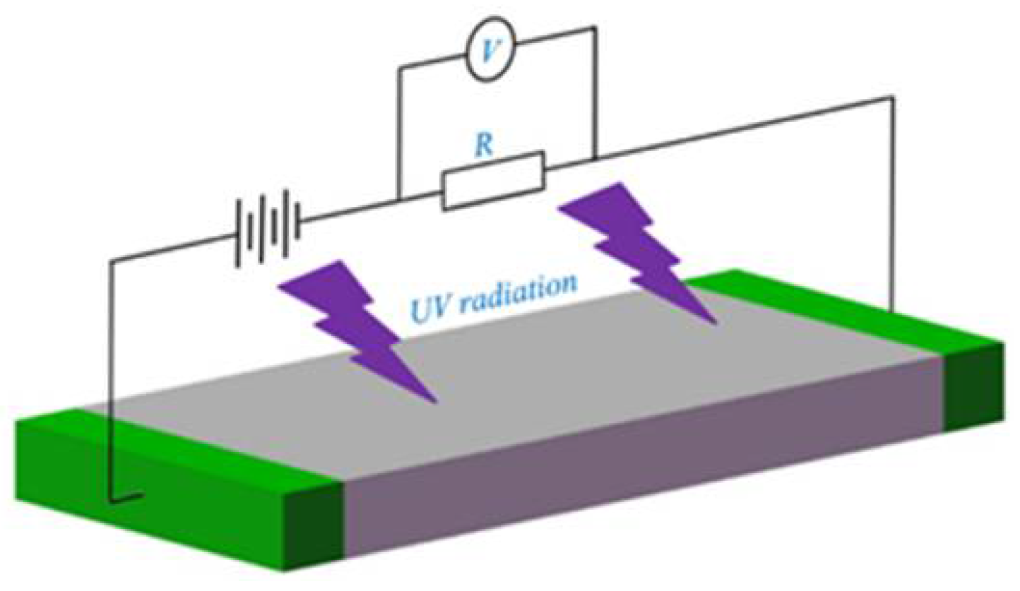
2.1. Photoconductive Detectors
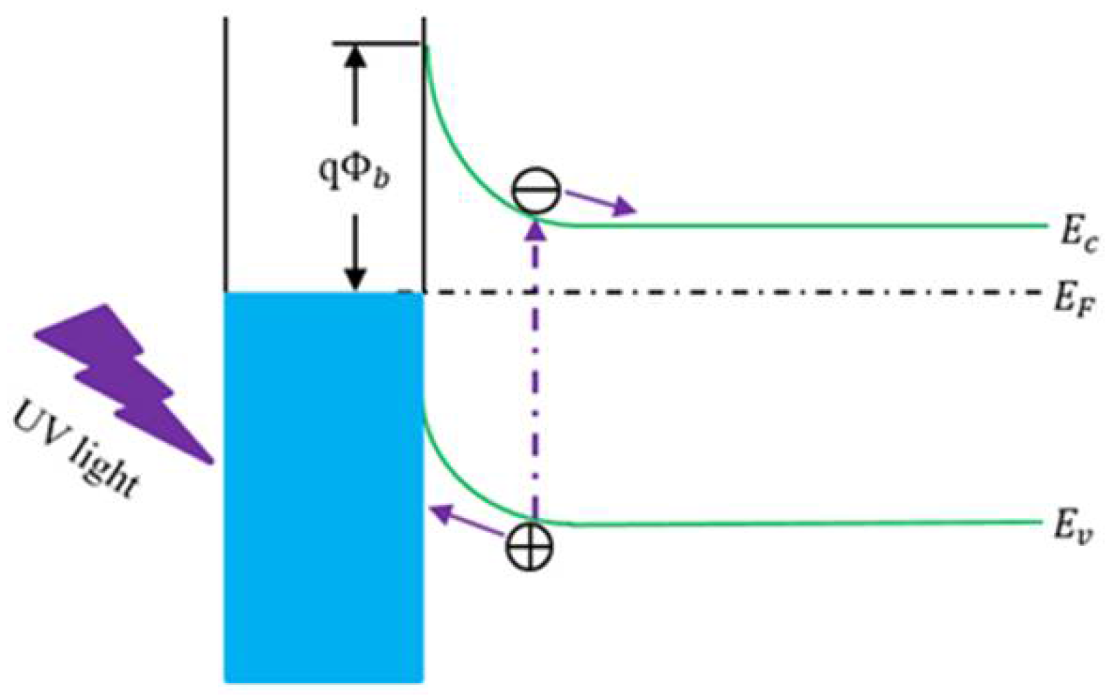
2.2. Schottky Detectors
2.3. p-n and p-i-n Junction Detectors
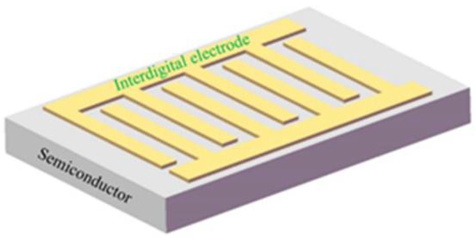
2.4. MSM Detectors
2.5. Important Parameters of UV Detector Devices
- Cut-off wavelength: The longest wavelength () that the UV detector can detect, referring to Equation (2) [48]. It can be measured by absorption and a transmittance spectrum, where h is Planck’s constant, c is the speed of light and is the band gap:
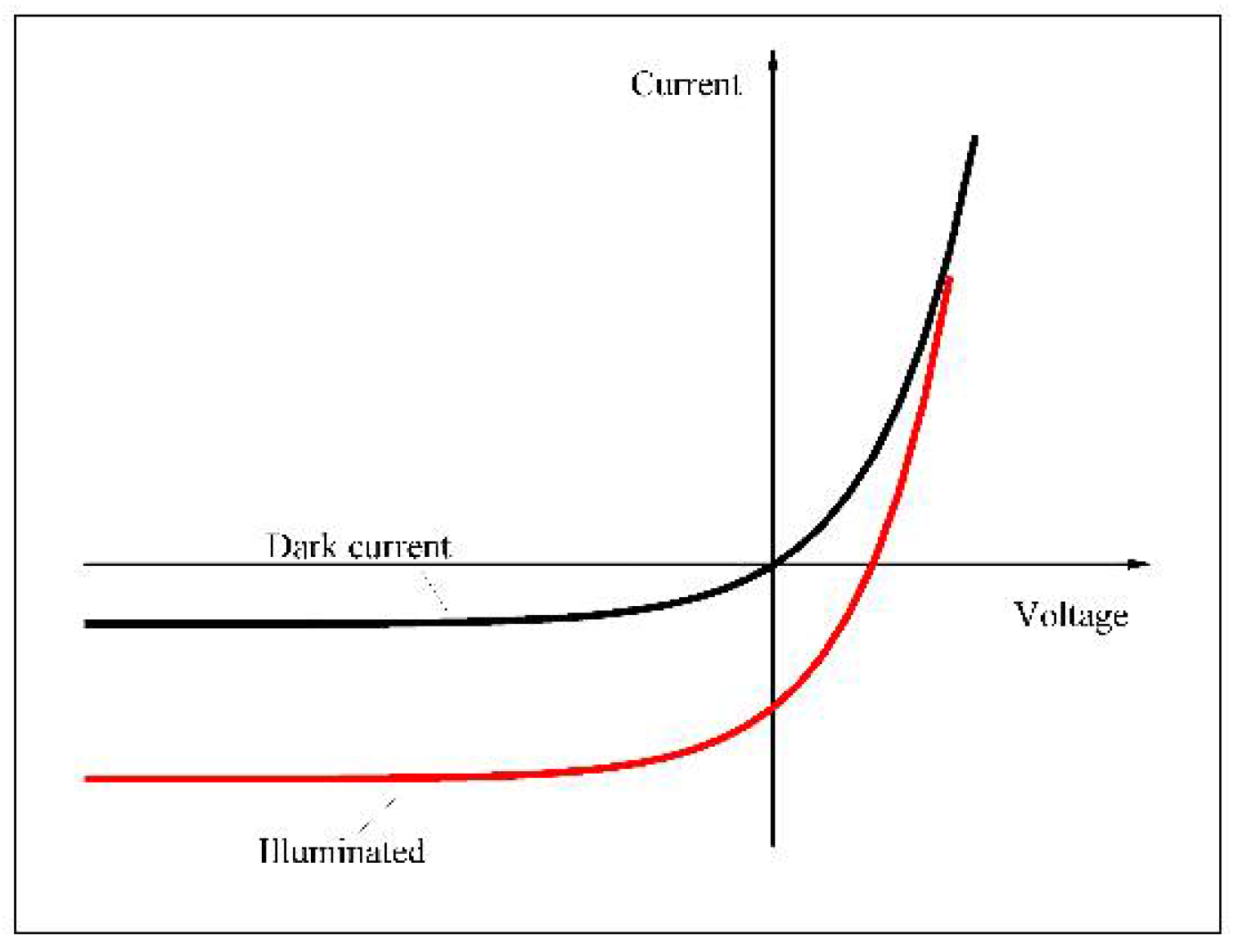
- Photocurrent: The current formed in the external circuit. It can be tested at different biases, I-V measurement under UV radiation, visible light and dark conditions.
- Dark current: The current which remains in the detector without UV radiation. Dark current is equivalent to a noise source and will weaken the signal-to-noise ratio.
- Time response: When the UV light turns on or off, the required time of the output value rises to become stable or decreases to the value before irradiation, accordingly. This implies the sensitivity of the device.
- Quantum efficiency: Every incident UV photon will try to produce an electron-hole; however, the number of created electron-hole pairs is usually less than the number of photons. This represents the quantum efficiency, which can be calculated by [49]:where is the measured responsivity at incident light wavelength , and q is the electron charge.
3. Materials for UV Detectors
3.1. Metal Oxides
3.1.1. ZnO
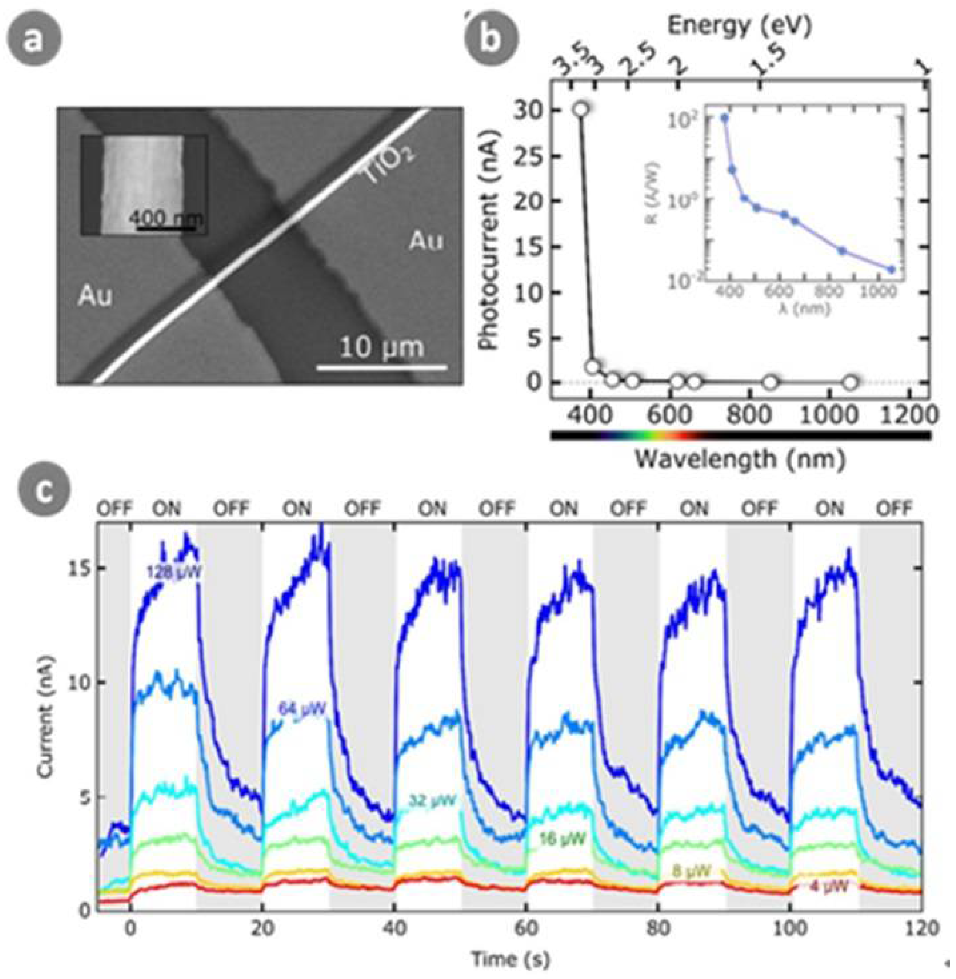
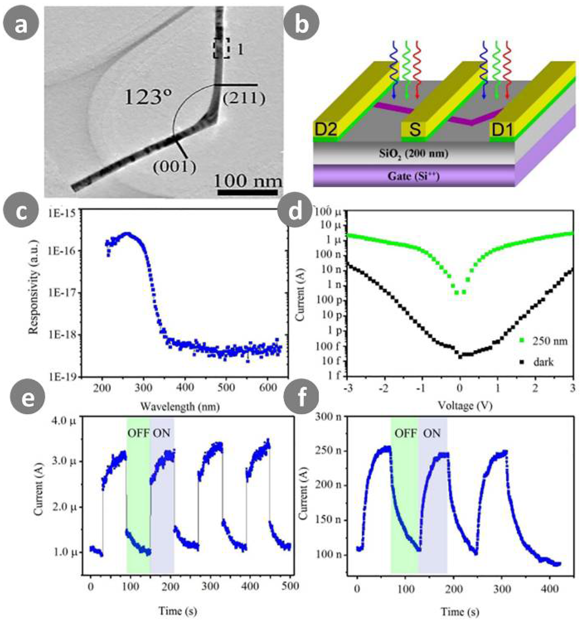
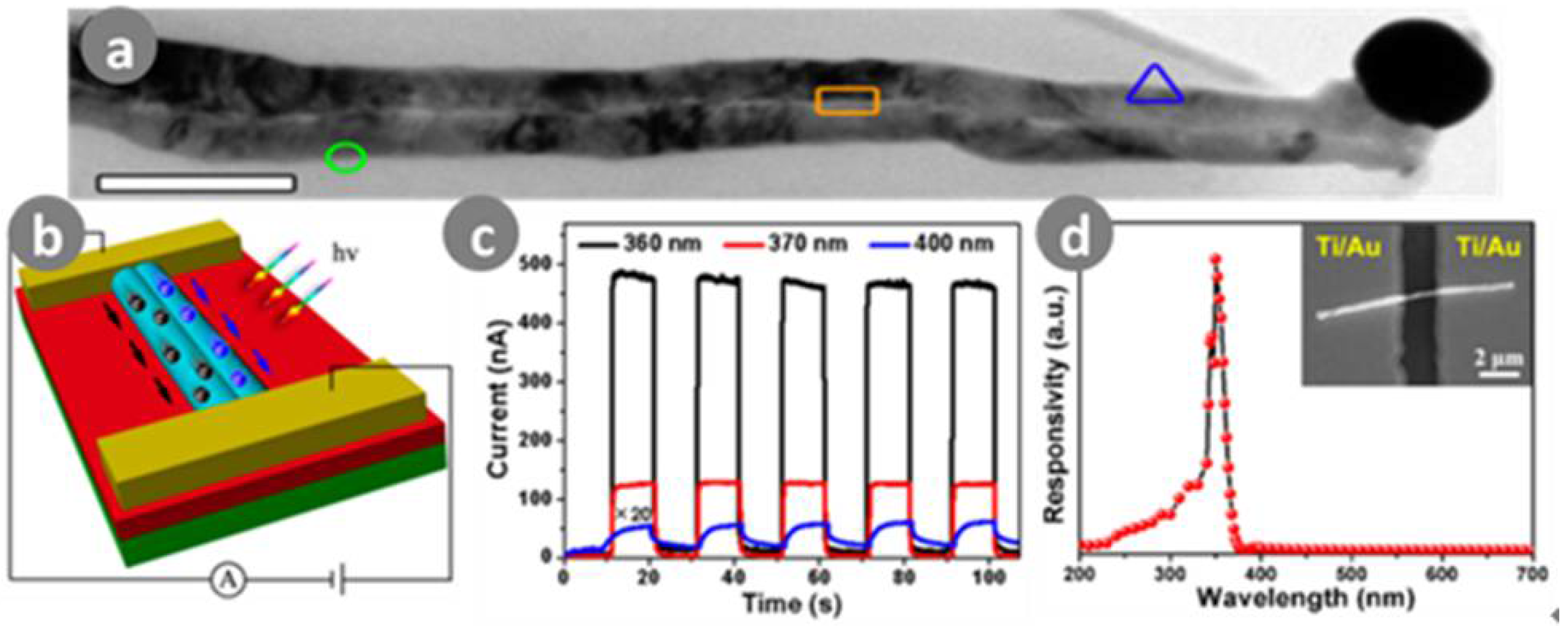
3.1.2. TiO2
3.1.3. SnO2
3.1.4. Others
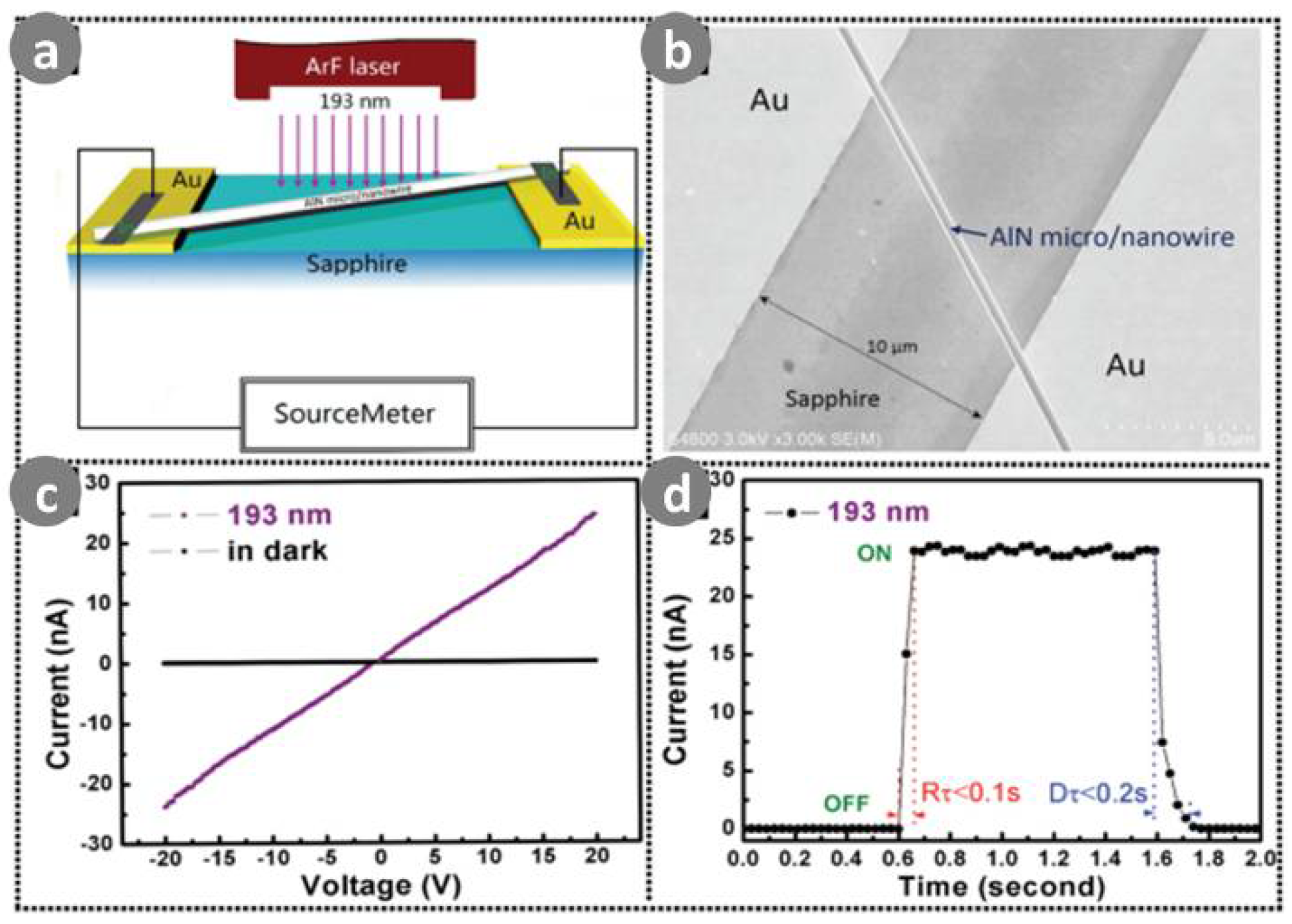
3.2. III-Nitride Semiconductors
3.3. SiC
3.4. Conclusions
4. New Types of UV Dtectors
4.1. Hybrid Nanostructure UV Detectors
4.2. Self-Powered UV Detectors
4.3. Flexible UV Detectors
5. Summary and Outlook
Author Contributions
Funding
Acknowledgments
Conflicts of Interest
References
- Delor, M.; Scattergood, P.A.; Sazanovich, I.V.; Parker, A.W.; Greetham, G.M.; Meijer, A.J.H.M.; Towrie, M.; Weinstein, J.A. Toward control of electron transfer in donor-acceptor molecules by bond-specific infrared excitation. Science 2014, 346, 1492–1495. [Google Scholar] [CrossRef] [PubMed]
- Di, W.; Hu, Q.; Yan, Z.; Chen, W.; Yan, C.; Huang, X.; Zhang, J.; Yang, P.; Deng, H.; Wang, J.; et al. Structural basis of ultraviolet-b perception by UVR8. Nature 2012, 484, 214–219. [Google Scholar] [CrossRef] [PubMed]
- Premi, S.; Wallisch, S.; Mano, C.M.; Weiner, A.B.; Bacchiocchi, A.; Wakamatsu, K.; Bechara, E.J.H.; Halaban, R.; Douki, T.; Brash, D.E. Chemiexcitation of melanin derivatives induces DNA photoproducts long after UV exposure. Science 2015, 347, 842–847. [Google Scholar] [CrossRef] [PubMed] [Green Version]
- Chen, H.; Liu, K.; Hu, L.; Al-Ghamdi, A.A.; Fang, X. New concept ultraviolet photodetectors. Mater. Today 2015, 18, 493–502. [Google Scholar] [CrossRef]
- Lei, S.N.S. Comparative Study of Silicon-Based Ultraviolet Photodetectors. IEEE Sens. J. 2012, 12, 2453–2459. [Google Scholar]
- Li, W.-D.; Chou, S.Y. Solar-blind deep-UV band-pass filter (250–350 nm) consisting of a metal nano-grid fabricated by nanoimprint lithography. Opt. Express 2010, 18, 931–937. [Google Scholar] [CrossRef] [PubMed]
- Alaie, Z.; Mohammad Nejad, S.; Yousefi, M.H. Recent advances in ultraviolet photodetectors. Mater. Sci. Semicond. Process. 2015, 29, 16–55. [Google Scholar] [CrossRef]
- Zhao, S.; Nguyen, H.P.T.; Kibria, M.G.; Mi, Z. III-Nitride nanowire optoelectronics. Prog. Quantum Electron. 2015, 44, 14–68. [Google Scholar] [CrossRef]
- Ponce, F.A.; Bour, D.P. Nitride-based semiconductors for blue and green light-emitting devices. Nature 1997, 386, 351–359. [Google Scholar] [CrossRef]
- Pengfei, T.; Ahmad, A.; Erdan, G.; Ian, M.W.; Martin, D.D.; Ran, L. Aging characteristics of blue InGaN micro-light emitting diodes at an extremely high current density of 3.5 kA cm−2. Semicond. Sci. Technol. 2016, 31, 045005. [Google Scholar]
- Morkoç, H.; Strite, S.; Gao, G.B.; Lin, M.E.; Sverdlov, B.; Burns, M. Large-band-gap SiC, III-V nitride, and II-VI ZnSe-based semiconductor device technologies. J. Appl. Phys. 1994, 76, 1363–1398. [Google Scholar] [CrossRef]
- Huang, M.H.; Mao, S.; Feick, H.; Yan, H.; Wu, Y.; Kind, H.; Weber, E.; Russo, R.; Yang, P. Room-Temperature Ultraviolet Nanowire Nanolasers. Science 2001, 292, 1897–1899. [Google Scholar] [CrossRef] [PubMed]
- Kind, H.; Yan, H.; Messer, B.; Law, M.; Yang, P. Nanowire ultraviolet photodetectorsand optical switches. Adv. Mater. 2002, 14, 158–160. [Google Scholar] [CrossRef]
- Bai, S.; Wu, W.; Qin, Y.; Cui, N.; Bayerl, D.J.; Wang, X. High-Performance Integrated ZnO Nanowire UV Sensors on Rigid and Flexible Substrates. Adv. Funct. Mater. 2011, 21, 4464–4469. [Google Scholar] [CrossRef]
- Soci, C.; Zhang, A.; Xiang, B.; Dayeh, S.A.; Aplin, D.P.R.; Park, J.; Bao, X.Y.; Lo, Y.H.; Wang, D. ZnO Nanowire UV Photodetectors with High Internal Gain. Nano Lett. 2007, 7, 1003–1009. [Google Scholar] [CrossRef] [PubMed] [Green Version]
- Chong, H.; Yang, H.; Yang, W.; Zheng, J.; Shang, M.; Yang, Z.; Wei, G.; Gao, F. SiC Nanowire Film Photodetectors: A Promising Candidate Toward High Temperature Photodetectors. J. Nanosci. Nanotechnol. 2016, 16, 3796–3801. [Google Scholar] [CrossRef] [PubMed]
- Johnson, J.C.; Choi, H.-J.; Knutsen, K.P.; Schaller, R.D.; Yang, P.; Saykally, R.J. Single gallium nitride nanowire lasers. Nat. Mater. 2002, 1, 106–110. [Google Scholar] [CrossRef] [PubMed]
- Pauporté, T.; Lupan, O.; Viana, B. Electrochemical and Hydrothermal Synthesis of Epitaxial Arrays of Doped ZnO Nanowire Emitters for Light Emitting Diodes With Tunable Emission From Near-UV to Blue. ECS Trans. 2013, 58, 17–22. [Google Scholar] [CrossRef]
- Eddy, C.R.; Nepal, N.; Hite, J.K.; Mastro, M.A. Perspectives on future directions in III-N semiconductor research. J. Vac. Sci. Technol. A 2013, 31, 058501. [Google Scholar] [CrossRef]
- Yang, Z.; Wang, D.; Meng, C.; Wu, Z.; Wang, Y.; Ma, Y.; Dai, L.; Liu, X.; Hasan, T.; Liu, X.; et al. Broadly Defining Lasing Wavelengths in Single Bandgap-Graded Semiconductor Nanowires. Nano Lett. 2014, 14, 3153–3159. [Google Scholar] [CrossRef] [PubMed] [Green Version]
- Arafin, S.; Liu, X.; Mi, Z. Review of recent progress of III-nitride nanowire lasers. J. Nanophotonics 2013, 7, 074599. [Google Scholar] [CrossRef] [Green Version]
- Lee, S.K.; Kim, T.H.; Lee, S.Y.; Choi, K.C.; Yang, P. High-brightness gallium nitride nanowire UV–blue light emitting diodes. Philos. Mag. 2007, 87, 2105–2115. [Google Scholar] [CrossRef]
- Pearton, S.J.; Norton, D.P.; Ren, F. The promise and perils of wide-bandgap semiconductor nanowires for sensing, electronic, and photonic applications. Small 2007, 3, 1144–1150. [Google Scholar] [CrossRef] [PubMed]
- Li, D.; Sun, X.; Song, H.; Li, Z.; Chen, Y.; Jiang, H.; Miao, G. Realization of a high-performance GaN UV detector by nanoplasmonic enhancement. Adv. Mater. 2012, 24, 845–849. [Google Scholar] [CrossRef] [PubMed]
- Hennessy, J.; Jewell, A.D.; Hoenk, M.E.; Nikzad, S. Metal-dielectric filters for solar-blind silicon ultraviolet detectors. Appl. Opt. 2015, 54, 3507–3512. [Google Scholar] [CrossRef] [PubMed]
- Liu, H.; She, G.; Mu, L.; Shi, W. Porous SiC nanowire arrays as stable photocatalyst for water splitting under UV irradiation. Mater. Res. Bull. 2012, 47, 917–920. [Google Scholar] [CrossRef]
- Oksenberg, E.; Popovitz-Biro, R.; Rechav, K.; Joselevich, E. Guided Growth of Horizontal ZnSe Nanowires and their Integration into High-Performance Blue-UV Photodetectors. Adv. Mater. 2015, 27, 3999–4005. [Google Scholar] [CrossRef] [PubMed] [Green Version]
- Peng, L.; Hu, L.; Fang, X. Low-dimensional nanostructure ultraviolet photodetectors. Adv. Mater. 2013, 25, 5321–5328. [Google Scholar] [CrossRef] [PubMed]
- Razeghi, M.; Rogalski, A. Semiconductor ultraviolet detectors. J. Appl. Phys. 1996, 79, 7433–7473. [Google Scholar] [CrossRef]
- Lincke, R.; Wilkerson, T.D. New Detector for the Vacuum Ultraviolet. Rev. Sci. Instrum. 1962, 33, 911–913. [Google Scholar] [CrossRef]
- Monroy, E.; Calle, F.; Pau, J.L.; Muñoz, E.; Omnès, F.; Beaumont, B.; Gibart, P. AlGaN-based UV photodetectors. J. Cryst. Growth 2001, 230, 537–543. [Google Scholar] [CrossRef]
- Liu, K.; Sakurai, M.; Aono, M. ZnO-based ultraviolet photodetectors. Sensors 2010, 10, 8604–8634. [Google Scholar] [CrossRef] [PubMed]
- Han, S. New developments in photoconductive detectors (invited). Rev. Sci. Instrum. 1997, 68, 647–652. [Google Scholar] [CrossRef]
- Putley, E.H. Indium Antimonide Submillimeter Photoconductive Detectors. Appl. Opt. 1965, 4, 649–657. [Google Scholar] [CrossRef]
- Takahashi, S.; Abe, T.; Nakagawa, A.; Kamata, S.; Chiba, T.; Nakagawa, M.; Kashiwaba, Y.; Chiba, S.; Endo, H.; Meguro, K.; et al. Applicability of nitrogen-doped ZnO single crystals for photoconductive type UV sensors. Phys. Status Solidi C 2014, 11, 1304–1307. [Google Scholar] [CrossRef]
- Xu, Y.; Cheng, C.; Du, S.; Yang, J.; Yu, B.; Luo, J.; Yin, W.; Li, E.; Dong, S.; Ye, P.; et al. Contacts between Two- and Three-Dimensional Materials: Ohmic, Schottky, and p–n Heterojunctions. ACS Nano 2016, 10, 4895–4919. [Google Scholar] [CrossRef] [PubMed]
- Zahedi, F.; Dariani, R.S.; Rozati, S.M. Ultraviolet photoresponse properties of ZnO: N/p-Si and ZnO/p-Si heterojunctions. Sens. Actuators A Phys. 2013, 199, 123–128. [Google Scholar] [CrossRef]
- Zhao, Y.; Qi, J.; Biswas, C.; Li, F.; Zhang, K.; Li, X.; Zhang, Y. Local irradiation effects of one-dimensional ZnO based self-powered asymmetric Schottky barrier UV photodetector. Mater. Chem. Phys. 2015, 166, 116–121. [Google Scholar] [CrossRef]
- Liu, W.W.; Yao, B.; Li, B.H.; Li, Y.F.; Zheng, J.; Zhang, Z.Z.; Shan, C.X.; Zhang, J.Y.; Shen, D.Z.; Fan, X.W. MgZnO/ZnO p–n junction UV photodetector fabricated on sapphire substrate by plasma-assisted molecular beam epitaxy. Solid State Sci. 2010, 12, 1567–1569. [Google Scholar] [CrossRef]
- Leung, Y.H.; He, Z.B.; Luo, L.B.; Tsang, C.H.A.; Wong, N.B.; Zhang, W.J.; Lee, S.T. ZnO nanowires array p-n homojunction and its application as a visible-blind ultraviolet photodetector. Appl. Phys. Lett. 2010, 96, 53102. [Google Scholar] [CrossRef]
- Bie, Y.-Q.; Liao, Z.-M.; Zhang, H.-Z.; Li, G.-R.; Ye, Y.; Zhou, Y.-B.; Xu, J.; Qin, Z.-X.; Dai, L.; Yu, D.-P. Self-powered, ultrafast, visible-blind UV detection and optical logical operation based on zno/gan nanoscale p-n junctions. Adv. Mater. 2011, 23, 649–653. [Google Scholar] [CrossRef] [PubMed]
- Shi, L.; Wang, F.; Li, B.; Chen, X.; Yao, B.; Zhao, D.; Shen, D. A highly efficient UV photodetector based on a zno microwire p-n homojunction. J. Mater. Chem. C 2014, 2, 5005–5010. [Google Scholar] [CrossRef]
- Cai, J.; Chen, X.; Hong, R.; Yang, W.; Wu, Z. High-performance 4H-SiC-based p-i-n ultraviolet photodiode and investigation of its capacitance characteristics. Opt. Commun. 2014, 333, 182–186. [Google Scholar] [CrossRef]
- Bugallo Ade, L.; Tchernycheva, M.; Jacopin, G.; Rigutti, L.; Julien, F.H.; Chou, S.T.; Lin, Y.T.; Tseng, P.H.; Tu, L.W. Visible-blind photodetector based on p-i-n junction GaN nanowire ensembles. Nanotechnology 2010, 21, 315201. [Google Scholar] [CrossRef] [PubMed]
- Inamdar, S.; Ganbavle, V.; Shaikh, S.; Rajpure, K. Effect of the buffer layer on the metal–semiconductor–metal UV photodetector based on Al-doped and undoped ZnO thin films with different device structures. Phys. Status Solidi A 2015, 212, 1704–1712. [Google Scholar] [CrossRef]
- Singh, S. Al doped ZnO based metal–semiconductor–metal and metal–insulator–semiconductor–insulator–metal UV sensors. Opt. Int. J. Light Electron. Opt. 2016, 127, 3523–3526. [Google Scholar] [CrossRef]
- Menzel, A.; Subannajui, K.; Güder, F.; Moser, D.; Paul, O.; Zacharias, M. Multifunctional ZnO-Nanowire-Based Sensor. Adv. Funct. Mater. 2011, 21, 4342–4348. [Google Scholar] [CrossRef]
- Peng, G.; Zhou, Y.; He, Y.; Yu, X.; Zhang, X.A.; Li, G.Y.; Haick, H. UV-induced SiC nanowire sensors. J. Phys. D Appl. Phys. 2015, 48, 055102. [Google Scholar] [CrossRef]
- Zhao, B.; Wang, F.; Chen, H.; Wang, Y.; Jiang, M.; Fang, X.; Zhao, D. Solar-Blind Avalanche Photodetector Based On Single ZnO–Ga2O3 Core–Shell Microwire. Nano Lett. 2015, 15, 3988–3993. [Google Scholar] [CrossRef] [PubMed]
- Shen, G.Z.; Chen, D. One-dimensional nanostructures for photodetectors. Recent Pat. Nanotechnol. 2010, 4, 20–31. [Google Scholar] [CrossRef] [PubMed]
- Özgür, Ü.; Alivov, Y.I.; Liu, C.; Teke, A.; Reshchikov, M.A.; Doğan, S.; Avrutin, V.; Cho, S.-J.; Morkoç, H. A comprehensive review of zno materials and devices. J. Appl. Phys. 2005, 98, 041301. [Google Scholar] [CrossRef]
- Yang, P.; Yan, H.; Mao, S.; Russo, R.; Johnson, J.; Saykally, R.; Morris, N.; Pham, J.; He, R.; Choi, H.J. Controlled growth of zno nanowires and their optical properties. Adv. Funct. Mater. 2002, 12, 323–331. [Google Scholar] [CrossRef]
- Bagnall, D.M.; Chen, Y.F.; Zhu, Z.; Yao, T.; Koyama, S.; Shen, M.Y.; Goto, T. Optically pumped lasing of zno at room temperature. Appl. Phys. Lett. 1997, 70, 2230–2232. [Google Scholar] [CrossRef]
- Repins, I.; Contreras, M.A.; Egaas, B.; DeHart, C.; Scharf, J.; Perkins, C.L.; To, B.; Noufi, R. 19.9%-efficient ZnO/CdS/CuInGaSe2 solar cell with 81.2% fill factor. Prog. Photovolt. Res. Appl. 2008, 16, 235–239. [Google Scholar] [CrossRef]
- Bai, X.; Wang, L.; Zong, R.; Lv, Y.; Sun, Y.; Zhu, Y. Performance Enhancement of ZnO Photocatalyst via Synergic Effect of Surface Oxygen Defect and Graphene Hybridization. Langmuir 2013, 29, 3097–3105. [Google Scholar] [CrossRef] [PubMed]
- Liao, S.-H.; Jhuo, H.-J.; Cheng, Y.-S.; Chen, S.-A. Fullerene Derivative-Doped Zinc Oxide Nanofilm as the Cathode of Inverted Polymer Solar Cells with Low-Bandgap Polymer (PTB7-Th) for High Performance. Adv. Mater. 2013, 25, 4766–4771. [Google Scholar] [CrossRef] [PubMed]
- Cheng, W.; Tang, L.; Xiang, J.; Ji, R.; Zhao, J. An extreme high-performance ultraviolet photovoltaic detector based on a ZnO nanorods/phenanthrene heterojunction. RSC Adv. 2016, 6, 12076–12080. [Google Scholar] [CrossRef]
- Zhou, J.; Gu, Y.; Hu, Y.; Mai, W.; Yeh, P.-H.; Bao, G.; Sood, A.K.; Polla, D.L.; Wang, Z.L. Gigantic enhancement in response and reset time of zno UV nanosensor by utilizing schottky contact and surface functionalization. Appl. Phys. Lett. 2009, 94, 191103. [Google Scholar] [CrossRef] [PubMed]
- Singh, S.K.; Hazra, P.; Tripathi, S.; Chakrabarti, P. Performance analysis of RF-sputtered ZnO/Si heterojunction UV photodetectors with high photo-responsivity. Superlattices Microstruct. 2016, 91, 62–69. [Google Scholar] [CrossRef]
- Liang, S.; Sheng, H.; Liu, Y.; Huo, Z.; Lu, Y.; Shen, H. ZnO Schottky ultraviolet photodetectors. J. Cryst. Growth 2001, 225, 110–113. [Google Scholar] [CrossRef]
- Das, S.N.; Moon, K.-J.; Kar, J.P.; Choi, J.-H.; Xiong, J.; Lee, T.I.; Myoung, J.-M. Zno single nanowire-based UV detectors. Appl. Phys. Lett. 2010, 97, 022103. [Google Scholar] [CrossRef]
- Liu, Y.; Gorla, C.R.; Liang, S.; Emanetoglu, N.; Lu, Y.; Shen, H.; Wraback, M. Ultraviolet detectors based on epitaxial zno films grown by mocvd. J. Electron. Mater. 2000, 29, 69–74. [Google Scholar] [CrossRef]
- Ji, L.W.; Peng, S.M.; Su, Y.K.; Young, S.J.; Wu, C.Z.; Cheng, W.B. Ultraviolet photodetectors based on selectively grown ZnO nanorod arrays. Appl. Phys. Lett. 2009, 94, 203106. [Google Scholar] [CrossRef]
- Su, Y.K.; Peng, S.M.; Ji, L.W.; Wu, C.Z.; Cheng, W.B.; Liu, C.H. Ultraviolet ZnO Nanorod Photosensors. Langmuir 2010, 26, 603–606. [Google Scholar] [CrossRef] [PubMed]
- Liu, B.; Wang, Z.; Dong, Y.; Zhu, Y.; Gong, Y.; Ran, S.; Liu, Z.; Xu, J.; Xie, Z.; Chen, D.; et al. Zno-nanoparticle-assembled cloth for flexible photodetectors and recyclable photocatalysts. J. Mater. Chem. 2012, 22, 9379–9384. [Google Scholar] [CrossRef]
- Chivukula, V.; Ciplys, D.; Shur, M.; Dutta, P. ZnO nanoparticle surface acoustic wave UV sensor. Appl. Phys. Lett. 2010, 96, 233512. [Google Scholar] [CrossRef]
- Lao, C.S.; Park, M.-C.; Kuang, Q.; Deng, Y.; Sood, A.K.; Polla, D.L.; Wang, Z.L. Giant enhancement in UV response of zno nanobelts by polymer surface-functionalization. J. Am. Chem. Soc. 2007, 129, 12096–12097. [Google Scholar] [CrossRef] [PubMed]
- Cao, B.Q.; Matsumoto, T.; Matsumoto, M.; Higashihata, M.; Nakamura, D.; Okada, T. ZnO Nanowalls Grown with High-Pressure PLD and Their Applications as Field Emitters and UV Detectors. J. Phys. Chem. C 2009, 113, 10975–10980. [Google Scholar] [CrossRef]
- Sharma, P.; Sreenivas, K. Highly sensitive ultraviolet detector based on ZnO/LiNbO3 hybrid surface acoustic wave filter. Appl. Phys. Lett. 2003, 83, 3617–3619. [Google Scholar] [CrossRef]
- Mallampati, B.; Nair, S.V.; Ruda, H.E.; Philipose, U. Role of surface in high photoconductive gain measured in ZnO nanowire-based photodetector. J. Nanopart. Res. 2015, 17, 176–186. [Google Scholar] [CrossRef]
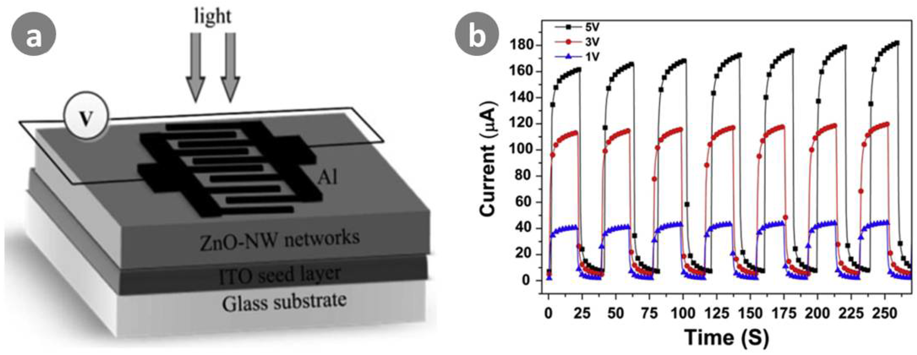
- Alsultany Forat, H.; Hassan, Z.; Ahmed Naser, M. A high-sensitivity, fast-response, rapid-recovery UV photodetector fabricated based on catalyst-free growth of ZnO nanowire networks on glass substrate. Opt. Mater. 2016, 60, 30–37. [Google Scholar] [CrossRef]
- Li, L.; Jiang, H.; Han, X.; Zhan, Z.; Du, H.; Lu, W.; Li, Z.; Taod, Z.; Fand, Y. Optimizing growth of ZnO nanowire networks for high-performance UV detection. Ceram. Int. 2017, 43, 15978–15985. [Google Scholar] [CrossRef]
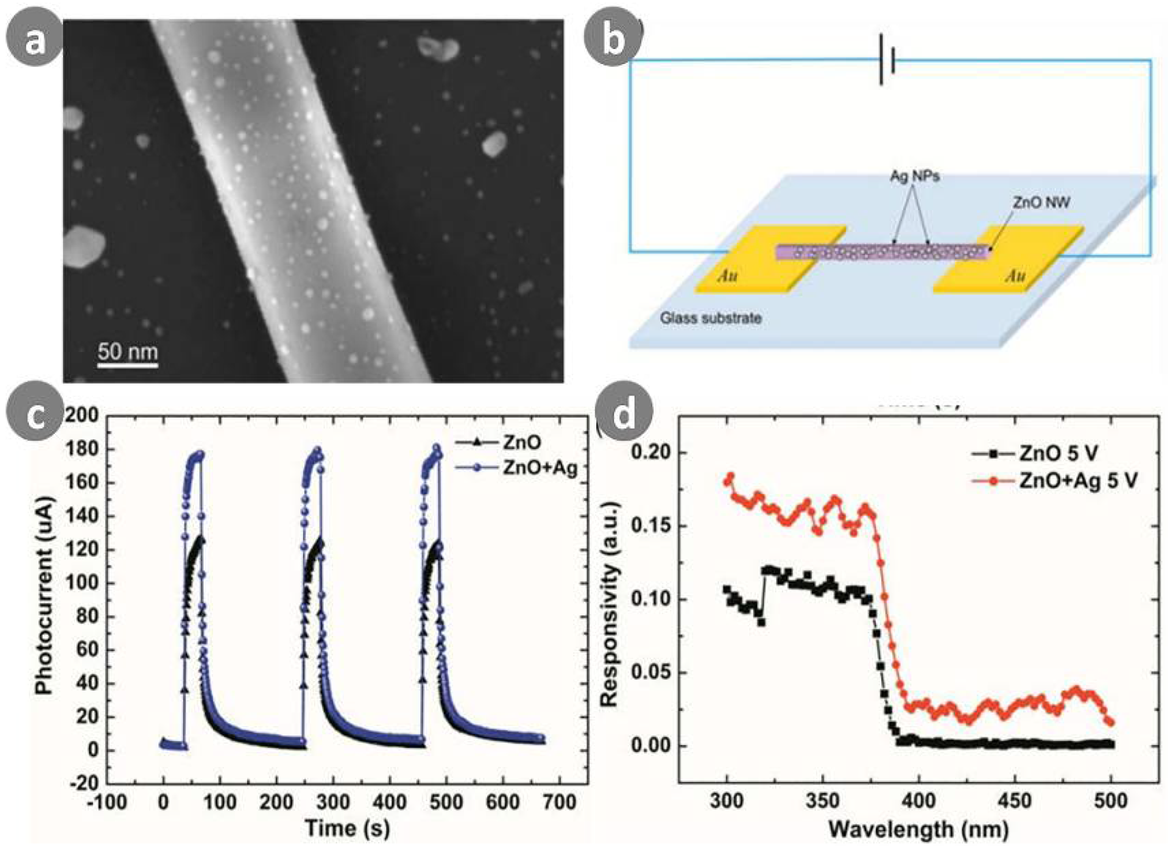
- Zhao, X.; Wang, F.; Shi, L.; Wang, Y.; Zhao, H.; Zhao, D. Performance enhancement in ZnO nanowire based double Shottky-Barriers photodetector by applying optimized Ag nanoparticles. RSC Adv. 2016, 6, 4634–4639. [Google Scholar] [CrossRef]
- Bonaccorso, F.; Sun, Z.; Hasan, T.; Ferrari, A.C. Graphene Photonics andOptoelectronics. Nat. Photonics 2010, 4, 611–622. [Google Scholar] [CrossRef]
- Liu, J.; Lu, R.; Xu, G.; Wu, J.; Thapa, P.; Moore, D. Development of a seedless floating growth process in solution for synthesis of crystalline ZnO micro/nanowire arrays on graphene: Towards high-performance nanohybrid ultraviolet photodetectors. Adv. Funct. Mater. 2013, 23, 4941–4948. [Google Scholar] [CrossRef]
- Boruah, B.D.; Mukherjee, A.; Sridhar, S.; Misra, A. Highly dense ZnO nanowires grown on graphene foam for ultraviolet photodetection. ACS Appl. Mater. Interfaces 2015, 7, 10606–10624. [Google Scholar] [CrossRef] [PubMed]
- Fu, Y.; Cao, W. Preparation of transparent TiO2 nanocrystalline film for UV sensor. Chin. Sci. Bull. 2006, 51, 1657–1661. [Google Scholar] [CrossRef]
- Jie, X.; Huiyun, W.; Er-Jia, G.; Fang, Y. Highly sensitive fast-response UV photodetectors based on epitaxial TiO2 films. J. Phys. D Appl. Phys. 2011, 44, 375104. [Google Scholar]
- Xie, Y.; Wei, L.; Wei, G.; Li, Q.; Wang, D.; Chen, Y.; Yan, S.; Liu, G.; Mei, L.; Jiao, J. A self-powered UV photodetector based on TiO2 nanorod arrays. Nanoscale Res. Lett. 2013, 8, 1–6. [Google Scholar] [CrossRef] [PubMed]
- Han, Y.; Wu, G.; Wang, M.; Chen, H. Hybrid ultraviolet photodetectors with high photosensitivity based on TiO2 nanorods array and polyfluorene. Appl. Surf. Sci. 2009, 256, 1530–1533. [Google Scholar] [CrossRef]
- Liu, G.; Zhang, M.; Zhang, D.; Gu, X.; Meng, F.; Wen, S.; Chen, Y.; Ruan, S. Effects of growth substrates on the morphologies of TiO2 nanowire arrays and the performance of assembled UV detectors. Appl. Surf. Sci. 2014, 315, 55–58. [Google Scholar] [CrossRef]
- Zhang, M.; Li, D.; Zhou, J.; Chen, W.; Ruan, S. Ultraviolet detector based on TiO2 nanowire array–polymer hybrids with low dark current. J. Alloys Compd. 2015, 618, 233–235. [Google Scholar] [CrossRef]
- Chen, S.P.; Retamal, J.R.D.; Lien, D.H.; He, J.H.; Liao, Y.C. Inkjet-printed transparent nanowire thin film features for UV photodetectors. RSC Adv. 2015, 5, 70707–70712. [Google Scholar] [CrossRef]
- Molina-Mendiza, A.J.; Moya, A.; Frisenda, R.; Svatek, S.A.; Gant, P.; Gonzalez-Abad, S.; Antolin, E.; Agraït, N.; Rubio-Bollinger, G.; de Lara, D.P.; et al. Highly responsive UV-photodetector based on single electrospun TiO2 nanofibres. J. Mater. Chem. C 2016, 4. [Google Scholar] [CrossRef]
- Luo, S.H.; Wan, Q.; Liu, W.L.; Zhang, M.; Di, Z.F.; Wang, S.Y.; Song, Z.T.; Lin, C.L.; Dai, J.Y. Vacuum electron field emission from SnO2 nanowhiskers synthesized by thermal evaporation. Nanotechnology 2004, 15, 1424–1427. [Google Scholar] [CrossRef]
- Comini, E.; Faglia, G.; Sberveglieria, G.; Pan, Z.; Wang, Z.L. Stable and highly sensitive gas sensors based on semiconducting oxide nanobelts. Appl. Phys. Lett. 2002, 81, 1869–1871. [Google Scholar] [CrossRef]
- Kim, H.W.; Shim, S.H. Synthesis and characteristics of SnO2 needle-shaped nanostructures. J. Alloys Compd. 2006, 426, 286–289. [Google Scholar] [CrossRef]
- Kim, H.W.; Lee, J.W.; Shim, S.H.; Lee, C. Controlled growth of SnO2 nanorods by thermal evaporation of Sn powder. J. Korean Phys. Soc. 2007, 51, 198–203. [Google Scholar] [CrossRef]
- Liu, Y.; Zheng, C.; Wang, W.; Yin, C.; Wang, G. Synthesis and characterization of rutile SnO2 nanorods. Adv. Mater. 2001, 13, 1883–1887. [Google Scholar] [CrossRef]
- Mathur, S.; Barth, S.; Shen, H.; Pyun, J.C.; Werner, U. Size-dependent photoconductance in SnO2 nanowires. Small 2005, 1, 713–717. [Google Scholar] [CrossRef] [PubMed]
- Hu, L.; Yan, J.; Liao, M.; Wu, L.; Fang, X. Ultrahign external quantum efficiency from thin SnO2 nanowire ultraviolet photodetectors. Small 2011, 7, 1012–1017. [Google Scholar] [CrossRef] [PubMed]
- Lu, M.L.; Lai, C.W.; Pan, H.J.; Chen, C.T.; Chou, P.T.; Chen, Y.F. A facile integration of zero-(I-II-VI quantum dots) and one-(single SnO2 nanowire) dimensional nanomaterials: Fabrication of a nanoconposite photodetector with ultrahigh gain and wide spectral response. Nano Lett. 2013, 13, 1920–1927. [Google Scholar] [CrossRef] [PubMed]
- Lupan, O.; Wolff, N.; Postica, V.; Braniste, T.; Paulowicz, I.; Hrkac, V.; Kumar, Y.; Tiginyanub, M.; Kienlea, L.; Adelunga, R.; et al. Properties of a single SnO2: Zn2SnO4-Functionalized nanowire based nanosensor. Ceram. Int. 2018, 44, 4859–4867. [Google Scholar] [CrossRef]
- Gan, L.; Liao, M.; Li, H.; Ma, Y.; Zhai, T. Geometry-induced hig performance of ultraviolet photodetectors in kinked SnO2nanowires. J. Mater. Chem. C 2015, 3, 8300–8306. [Google Scholar] [CrossRef]
- Wu, J.M.; Chang, W.E. Ultrahigh responsivity and external quantum efficiency of an ultraviolet-light photodetector based on a single VO2 microwore. ACS Appl. Mater. Interfaces 2014, 6, 14286–14292. [Google Scholar] [CrossRef] [PubMed]
- Du, J.; Xing, J.; Ge, C.; Liu, H.; Liu, P.; Hao, H.; Dong, J.; Zheng, Z.; Gao, H. Highly sensitive and ultrafast deep UV photodetector based on a β-Ga2O3 nanowire network grown by CVD. J. Phys. D Appl. Phys. 2016, 49, 425105–425112. [Google Scholar] [CrossRef]
- Meng, M.; Wu, X.; Ji, X.; Gan, Z.; Liu, L.; Shen, J.; Chu, P.K. Ultrahigh quantum efficiency photodetector and ultrafast reversible surface wettability transtion of square In2O3 nanowires. Nano Res. 2017, 10, 2772–2781. [Google Scholar] [CrossRef]
- Liu, H.; Zhang, Z.; Hu, L.; Gao, N.; Sang, L.; Liao, M.; Ma, R.; Xu, F.; Fang, X. New UV-A photodetector based on individual potassium niobate nanowires with high performance. Adv. Opt. Mater. 2014, 2, 771–778. [Google Scholar] [CrossRef]
- Lou, Z.; Li, L.; Shen, G. InGaO3(ZnO) superlattice nanowire for high-performance ultraviolet photodetectors. Adv. Electron. Mater. 2015, 1, 1500054–1500061. [Google Scholar] [CrossRef]
- Lou, Z.; Li, L.; Shen, G. High-performance rigid amd flexible ultraviolet photodetectors with single-crystalline ZnGa2O4 nanowires. Nano Res. 2015, 8, 2162–2169. [Google Scholar] [CrossRef]
- Zhou, X.; Zhang, Q.; Gan, L.; Li, X.; Li, H.; Zhang, Y. High -performance solar-blind deep ultraviolet photodetector bsed on individul single-crystalline Zn2GeO4 nanowire. Adv. Funct. Mater. 2016, 26, 704–712. [Google Scholar] [CrossRef]
- Khan, M.A.; Shatalov, M.; Maruska, H.P.; Wang, H.M.; Kuokstis, E. III–Nitride UV Devices. Jpn. J. Appl. Phys. 2005, 44, 7191–7206. [Google Scholar] [CrossRef] [Green Version]
- Wright, A.F. Elastic properties of zinc-blende and wurtzite AlN, GaN, and InN. J. Appl. Phys. 1997, 82, 2833–2839. [Google Scholar] [CrossRef]
- Yong, K.-T.; Yu, S.F. AlN nanowires: Synthesis, physical properties, and nanoelectronics applications. J. Mater. Sci. 2012, 47, 5341–5360. [Google Scholar]
- Wang, Q.; Connie, A.T.; Nguyen, H.P.; Kibria, M.G.; Zhao, S.; Sharif, S.; Shih, I.; Mi, Z. Highly efficient, spectrally pure 340 nm ultraviolet emission from AlxGa1-xN nanowire based light emitting diodes. Nanotechnology 2013, 24, 345201. [Google Scholar] [CrossRef] [PubMed]
- Zheng, W.; Huang, F.; Zheng, R.; Wu, H. Low-Dimensional Structure Vacuum-Ultraviolet-Sensitive (lambda < 200 nm) Photodetector with Fast-Response Speed Based on High-Quality AlN Micro/Nanowire. Adv. Mater. 2015, 27, 3921–3927. [Google Scholar] [PubMed]
- Reshchikov, M.A.; Morkoç, H. Luminescence properties of defects in GaN. J. Appl. Phys. 2005, 97, 061301. [Google Scholar] [CrossRef]
- Kim, M.-H.; Schubert, M.F.; Dai, Q.; Kim, J.K.; Schubert, E.F.; Piprek, J.; Park, Y. Origin of efficiency droop in GaN-based light-emitting diodes. Appl. Phys. Lett. 2007, 91, 183507. [Google Scholar] [CrossRef] [Green Version]
- Li, P.; Meng, X. Thermal annealing effects on the optoelectronic characteristics of fully nanowire-based UV detector. J. Mater. Sci. Mater. Electron. 2016, 27, 7693–7698. [Google Scholar] [CrossRef]
- Verheij, D.; Peres, M.; Cardoso, S.; Alves, L.C.; Alves, E.; Durand, C.; Eymery, J.; Lorenz, K. Radiation sensors based on GaN microwires. J. Phys. D Appl. Phys. 2018, 51, 175105. [Google Scholar] [CrossRef] [Green Version]
- Wang, X.; Zhang, Y.; Chen, X.; He, M.; Liu, C.; Yin, Y.; Zou, X.; Li, S. Ultrafast, superhigh gain visible-blind UV detector and optical logic gates based on nonpolar a-axial GaN nanowire. Nanoscale 2014, 6, 12009–12017. [Google Scholar] [CrossRef] [PubMed]
- Zhang, X.; Liu, Q.; Liu, B.; Yang, W.; Li, J.; Niu, P.; Jiang, X. Giant UV photorespomse of a GaN nanowire photodetector through effective Pt nanoparticle coupling. J. Mater. Chem. C 2017, 5, 4319–4326. [Google Scholar] [CrossRef]
- Zhang, X.; Liu, B.; Liu, Q.; Yang, W.; Xiong, C.; Li, J.; Jiang, X. Ultra sensitive and highly selective photodetections of UV-A rays based on individual bicrystalline GaN nanowire. ACS Appl. Mater. Interfaces 2017, 9, 2669–2677. [Google Scholar] [CrossRef] [PubMed]
- Liu, F.; Li, L.; Guo, T.; Gan, H.; Mo, X.; Chen, J.; Deng, S.; Xu, N. Investigation on the photoconductive behaviors of an individual AlN nanowire under different excited lights. Nanoscale Res. Lett. 2012, 7, 1–9. [Google Scholar] [CrossRef] [PubMed]
- Teker, K. Photoresponse characteristics of silicon carbide nanowires. Microelectron. Eng. 2016, 162, 79–81. [Google Scholar] [CrossRef]
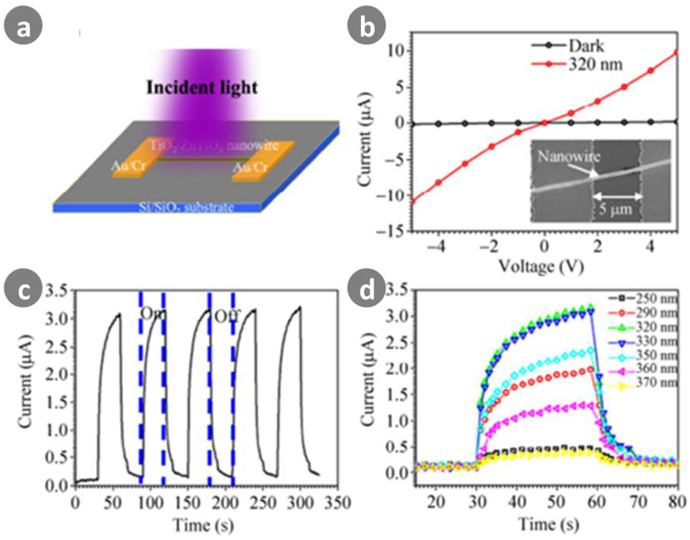
- Chong, H.; Wei, G.; Hou, H.; Yang, H.; Shang, M.; Gao, F.; Yang, W.; Shen, G. High-performance solar-blined ultraviolet photodetector based on electrispun TiO2-ZnTiO3 heterojunction nanowires. Nano Res. 2015, 8, 2822–2832. [Google Scholar] [CrossRef]
- Zhang, H.; Messanvi, A.; Durand, C.; Eymery, J.; Lavenus, P.; Babichev, A.; Julien, F.H.; Tchernycheva, M. InGaN/GaN core/shell nanowires for visible to ultraviolet range photodetection. Phys. Status Solidi A 2016, 213, 936–940. [Google Scholar] [CrossRef] [Green Version]
- Zhang, H.; Guan, N.; Piazza, V.; Kapoor, A.; Bougerol, C.; Julien, F.H.; Babichev, A.V.; Cavassilas, N.; Bescond, M.; Michelini, F.; et al. Comprehensive analyses of core-shell InGaN/GaN single nanowire photodiodes. J. Phys. D Appl. Phys. 2017, 50, 484001. [Google Scholar] [CrossRef]
- Rai, S.C.; Wang, K.; Ding, Y.; Marmon, J.K.; Bhatt, M.; Zhang, Y.; Zhou, W.; Wang, Z.L. Piezo-Phototronic Effect Enhanced UV/Visible Photodetector Based on Fully Wide Band Gap Type-II ZnO/ZnS Core/Shell Nanowire Array. ACS Nano 2015, 9, 6419–6427. [Google Scholar] [CrossRef] [PubMed]
- Park, S.; Kim, S.; Sun, G.-J.; Byeon, D.B.; Hyun, S.K.; Lee, W.I.; Lee, C. ZnO-core/ZnSe-shell nanowire UV photodetector. J. Alloys Compd. 2016, 658, 459–564. [Google Scholar] [CrossRef]
- Dao, T.D.; Dang, C.T.T.; Han, G.; Hoang, C.V.; Yi, W.; Narayanamurti, V.; Nagao, T. Chemically synthesized nanowire TiO2/ZnO core-shell p-n junction array for high sensitivity ultraviolet photodetector. Appl. Phys. Lett. 2013, 103, 193119. [Google Scholar] [CrossRef]
- Shin, D.S.; Cho, I.; Kim, T.G.; Jeong, S.H.; Park, J. Investigation of p-CuO/n-Cu1-xInxO core/shell nanowire structure performance in UV photodetectors. J. Alloys Compd. 2017, 728, 1180–1185. [Google Scholar] [CrossRef]
- Yang, S.; Tongay, S.; Li, S.S.; Xia, J.B.; Wu, J.; Li, J. Environmentally stable/self-powered ultraviolet photodetectors with high sensitivity. Appl. Phys. Lett. 2013, 103, 143503. [Google Scholar] [CrossRef]
- Chen, Z.; Li, B.; Mo, X.; Li, S.; Wen, J.; Lei, H.; Zhu, Z.; Yang, G.; Gui, P.; Yao, F.; et al. Self-powered narrowband p-NiO/n-ZnO nanowire ultraviolet photodetector with interface modification of Al2O3. Appl. Phys. Lett. 2017, 110, 123504. [Google Scholar] [CrossRef]
- Bai, Z.; Zhang, Y. Self-powered UV-visible photodetectors based on ZnO/Cu2O nanowire/electrolyte heterojunctions. J. Alloys Compd. 2016, 675, 325–330. [Google Scholar] [CrossRef]
- Bai, Z.; Liu, J.; Liu, F.; Zhang, Y. Enhanced photoresponse performance of self-powered UV-visible photodetectors based on ZnO/Cu2O/electrolyte heterojunctions via graphene incorporation. J. Alloys Compd. 2017, 726, 803–809. [Google Scholar] [CrossRef]
- Bai, Z.; Fu, M.; Zhang, Y. Vertically aligned and ordered ZnO/CdS nanowire arrays for self-powered UV-visible photosensing. J. Mater. Sci. 2017, 52, 1308–1317. [Google Scholar] [CrossRef]
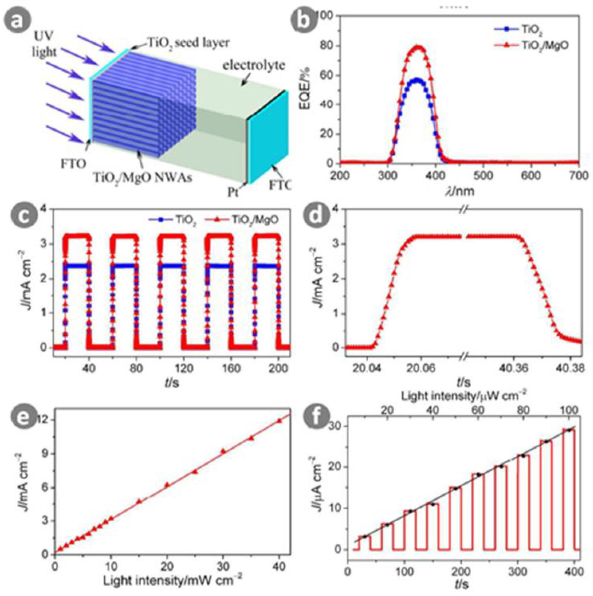
- Ni, S.; Yu, Q.; Hung, Y.; Wang, J.; Li, L.; Yu, C. Heterostructured TiO2/MgO nanowire arrays for self-powered UV photodetectors. RSC Adv. 2016, 6, 85951–85957. [Google Scholar] [CrossRef]
- Kim, D.; Shin, G.; Yoon, J.; Jang, D.; Lee, S.J.; Zi, G.; Ha, J.S. High performance stretchable UV sensor arrays of SnO2 nanowires. Nanotechnology 2013, 24, 315502. [Google Scholar] [CrossRef] [PubMed]
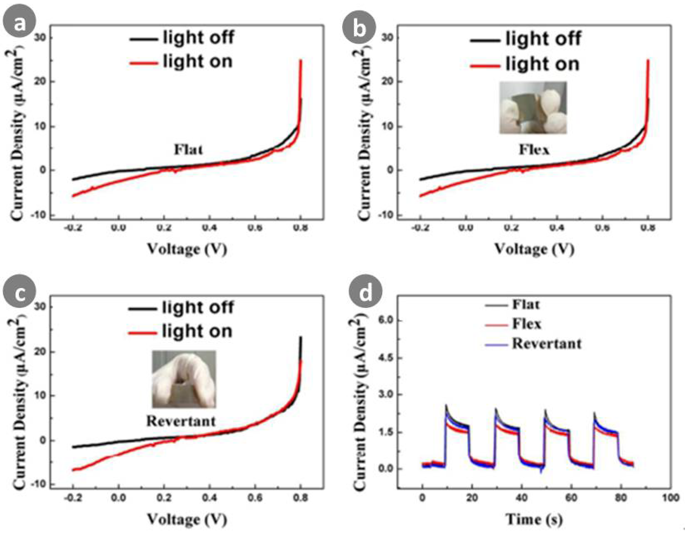
- Park, J.; Lee, J.; Noh, Y.; Shin, K.H.; Lee, D. Flexible ultraviolet photodetectors with ZnO nanowire net works fabricated by large area controlled roll-to-roll processing. J. Mater. Chem. C 2016, 34, 7948–7958. [Google Scholar] [CrossRef]
- Patel, D.B.; Patel, M.; Chauhan, K.R.; Kim, J.; Oh, M.S.; Kim, J.W. High-performing flexible and transparent photodetector by using silver nanowire-networks. Mater. Rese. Bull. 2018, 97, 244–250. [Google Scholar] [CrossRef]
- Zeng, Y.; Pan, X.; Lu, B.; Ye, Z. Fabrication of flexible self-powered UV detectors based on ZnO nanowires and the enhancement by the decoration of Ag nanoparticles. RSC Adv. 2016, 6, 31316–31322. [Google Scholar] [CrossRef]


| SiCPolytype | Bandgap at 300 K [eV] | Cut Off Wavelength [nm] | Electron Mobility [cm2V−1s−1] | Hole Mobility [cm2V−1s−1] |
|---|---|---|---|---|
| 3C | 2.36 | 525 | <800 | <320 |
| 4H | 3.23 | 384 | <900 | <120 |
| 6H | 3.05 | 407 | <400 | <90 |
| Materials of Nanowires | Light (nm) | Photocurrent (A) | Dark Current (A) | Responsivity (A/W) | EQE/Gain | Response Time (s) | Reference |
|---|---|---|---|---|---|---|---|
| ZnO | 370 | - | - | 105 | 108% | [70] | |
| ZnO | 365 | 1.79 × 10⁻⁴ | - | - | 2420% | 3.9 | [71] |
| ZnO | 365 | - | - | - | - | 0.45 | [72] |
| ZnO/Ag | 365 | - | - | 4.91 × 10⁶ | 1.67 × 10⁹% | - | [73] |
| ZnO/Graphene | - | 6.3 × 10⁻⁴ | - | 1.62 | - | 0.3 | [75] |
| ZnO/Graphene | - | - | - | - | 2490.8% | 9.5 | [76] |
| TiO2 (FTO) | 350 | 1.52 × 10⁻⁵ | 3.6 × 10⁻⁹ | 0.17 | 60.7% | [81] | |
| (ITO) | 3.37 × 10⁻⁶ | 2.36 × 10⁻⁸ | 0.38 | 13.4% | - | ||
| TiO2 | 330 | - | 1.9 × 10⁻⁹ | 5.68 × 10⁻¹ | - | - | [82] |
| TiO2 | - | 1.67 × 10⁻⁹ | 2 × 10⁻¹² | - | - | 0.4 | [83] |
| TiO2 | 375 | - | - | 90 | - | 5 | [84] |
| SnO2 | 320 | 2.1 × 10⁻⁶ | 1.94 ×10⁻⁸ | - | 1.32 × 10⁹% | - | [91] |
| SnO2 | 325 | - | - | - | 2.5 × 10⁷% | - | [92] |
| SnO2 | 365 | 2.3 × 10⁻⁶ | 2.1 × 10⁻⁷ | - | - | 0.1 | [93] |
| SnO2 | 250 | - | - | 1.2 × 10⁷ | 6.0 × 10⁹% | - | [94] |
| VO2 | 360–400 | - | - | 7.07 × 10³ | 2.4 × 10¹⁰% | 0.126 | [95] |
| β-Ga2O3 | 250 | - | - | 3.77 × 10² | 2 × 10⁵% | 1.2 × 10⁻⁶ | [96] |
| In2O3 | 405 | 2.17 × 10⁻² | 4.5 × 10⁻⁴ | 4.8 × 10⁶ | 1.46 × 10⁹% | 3 | [97] |
| K2Nb8O21 | 320 | 1.35 × 10⁻¹¹ | 1.2 × 10⁻¹² | 2.53 | 982% | <0.3 | [98] |
| InGaO3(ZnO) | 350 | 4.71 × 10⁻⁷ | 4.3 × 10⁻⁹ | 5.3 × 10⁴ | 1.9 × 10⁹% | 0.3 | [99] |
| ZnGa2O4 | 350 | 5.2 × 10⁻⁸ | 4 × 10⁻¹⁰ | 3.174 | 1.1 × 10⁶% | 15 | [100] |
| Zn2GeO4 | 260 | - | 1 × 10⁻⁹ | 5.11 × 10³ | 2.45 × 10⁸% | 0.01 | [101] |
| GaN | 325 | 10−8 | - | 2.2 × 10⁴ | 3.2 × 10⁷% | <0.026 | [111] |
| GaN/Pt | 380 | - | - | 6.39 × 10⁴ | 2.24 × 10⁷% | 1.1 | [112] |
| GaN | 320–400 | - | - | 1.74 × 10⁷ | 6.08 × 10⁹% | 0.144 | [113] |
| AlN | 325 | - | - | 2.7 × 10⁶ | - | 0.001 | [114] |
| AlN | 193 | 2.4 × 10⁻⁸ | 1 × 10⁻¹⁴ | 0.39 | 254% | <0.1 | [106] |
| SiC (Schottky) | - | 4.3 × 10⁻⁶ | 4.3 × 10⁻⁸ | - | - | [48] | |
| SiC | 254 | - | - | - | - | 3 | [115] |
© 2018 by the authors. Licensee MDPI, Basel, Switzerland. This article is an open access article distributed under the terms and conditions of the Creative Commons Attribution (CC BY) license (http://creativecommons.org/licenses/by/4.0/).
Share and Cite
Zou, Y.; Zhang, Y.; Hu, Y.; Gu, H. Ultraviolet Detectors Based on Wide Bandgap Semiconductor Nanowire: A Review. Sensors 2018, 18, 2072. https://doi.org/10.3390/s18072072
Zou Y, Zhang Y, Hu Y, Gu H. Ultraviolet Detectors Based on Wide Bandgap Semiconductor Nanowire: A Review. Sensors. 2018; 18(7):2072. https://doi.org/10.3390/s18072072
Chicago/Turabian StyleZou, Yanan, Yue Zhang, Yongming Hu, and Haoshuang Gu. 2018. "Ultraviolet Detectors Based on Wide Bandgap Semiconductor Nanowire: A Review" Sensors 18, no. 7: 2072. https://doi.org/10.3390/s18072072