The Fabrication and Characterization of InAlAs/InGaAs APDs Based on a Mesa-Structure with Polyimide Passivation

 ,
,
Abstract
:1. Introduction
2. Experiments
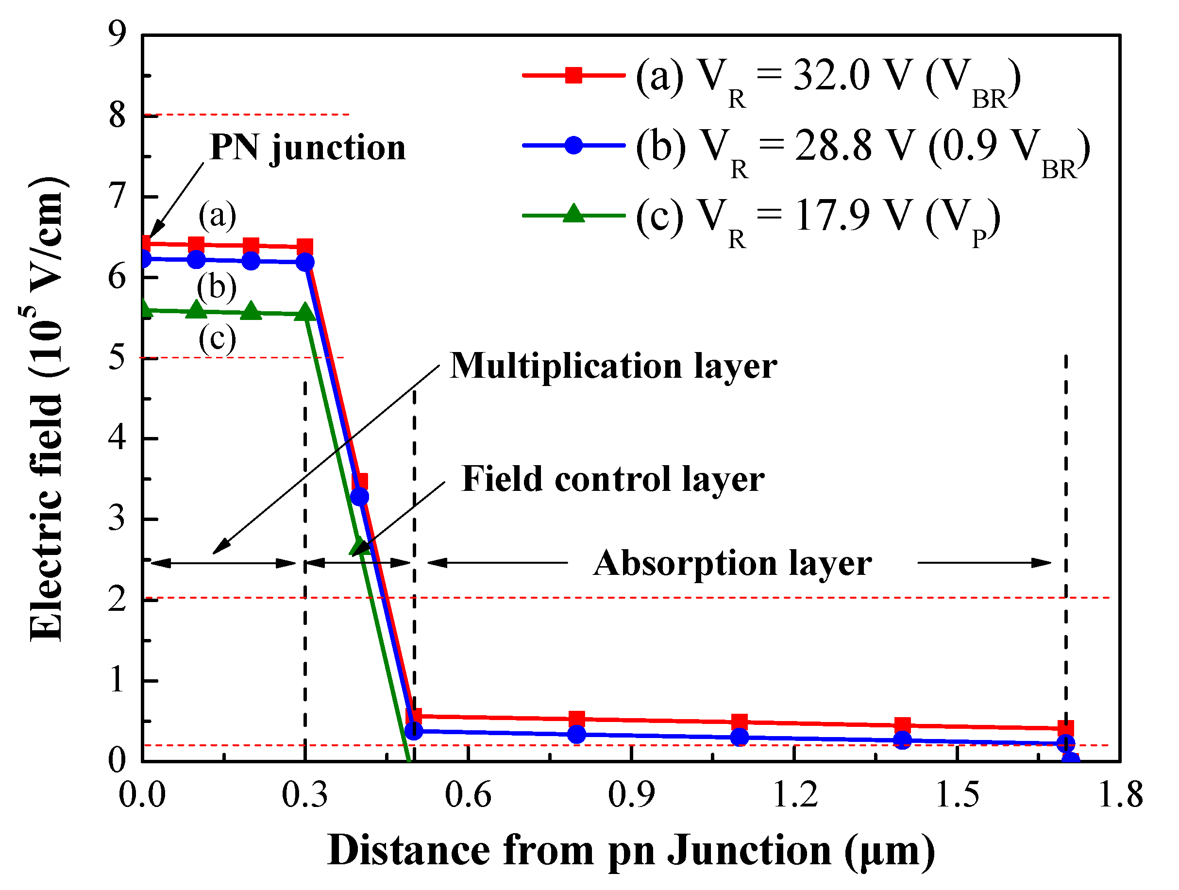
2.1. Epitaxial Layer Design and the Calculation of Electric-Field Profiles
2.2. Fabrication and Characterization of InAlAs/InGaAs APDs
2.3. Electric Field Profile Calculation
3. Results and Discussion
3.1. DC Characteristics of SAGFM APD
3.2. AC Characteristics of SAGFM APD
4. Conclusions
Author Contributions
Funding
Conflicts of Interest
References
- Murtaza, S.; Anselm, K.; Hu, C.; Nie, H.; Streetman, B.; Campbell, J. Resonant-cavity enhanced (RCE) separate absorption and multiplication (SAM) avalanche photodetector (APD). IEEE Photonics Technol. Lett. 1995, 7, 1486–1488. [Google Scholar] [CrossRef]
- Anselm, K.; Nie, H.; Hu, C.; Lenox, C.; Yuan, P.; Kinsey, G.; Campbell, J.; Streetman, B. Performance of thin separate absorption, charge, and multiplication avalanche photodiodes. IEEE J. Quantum Electron. 1998, 34, 482–490. [Google Scholar] [CrossRef]
- Zhao, Y.; Zhang, D.; Qin, L.; Tang, Q.; Wu, R.H.; Liu, J.; Zhang, Y.; Zhang, H.; Yuan, X.; Liu, W. InGaAs-InP avalanche photodiodes with dark current limited by generation-recombination. Opt. Express 2011, 19, 8546–8556. [Google Scholar] [CrossRef] [PubMed]
- Ribordy, G.; Gisin, N.; Guinnard, O.; Stucki, D.; Wegmuller, M.; Zbinden, H. Photon counting at telecom wavelengths with commercial InGaAs/InP avalanche photodiodes: current performance. J. Mod. Opt. 2004, 51, 1381–1398. [Google Scholar]
- Lee, M.H.; Ha, C.; Jeong, H.-S.; Kim, D.W.; Lee, S.H.; Lee, M.H.; Kim, K.H. Wavelength-division-multiplexed InGaAs/InP avalanched photodiodes for quantum key distributions. Opt. Commun. 2016, 361, 162–167. [Google Scholar] [CrossRef]
- Yu, Y.-J.; Bosman, G.; Bhattacharya, P.K. Impact ionization coefficient ratio in InGaAs/InAlAs superlattice avalanche photodiodes determined from noise measurements. Appl. Phys. Lett. 1987, 51, 1433–1435. [Google Scholar] [CrossRef] [Green Version]
- Goh, Y.L.; Massey, D.J.; Marshall, A.R.J.; Ng, J.S.; Tan, C.H.; Ng, W.K.; Rees, G.J.; Hopkinson, M.; David, J.P.R.; Jones, S.K. Avalanche Multiplication in InAlAs. IEEE Trans. Electron Devices 2007, 54, 11–16. [Google Scholar] [CrossRef]
- Capasso, F.; Mohammed, K.; Alavi, K.; Cho, A.Y.; Foy, P.W. Impact ionization rates for electrons and holes in Al0.48In0.52As. Appl. Phys. Lett. 1984, 45, 968–970. [Google Scholar] [CrossRef]
- Watanabe, I.; Torikai, T.; Makita, K.; Fukushima, K.; Uji, T. Impact ionization rates in (100) Al0.48In0.52As. IEEE Electron Device Lett. 1990, 11, 437–438. [Google Scholar] [CrossRef]
- Takanashi, Y.; Muramoto, Y.; Takahata, K. Characteristics of InAlAs/InGaAs high-electron-mobility transistors under illumination with modulated light. IEEE Trans. Electron Devices 1999, 46, 2271–2277. [Google Scholar] [CrossRef]
- Watanabe, T.; Boubanga-Tombet, S.A.; Tanimoto, Y.; Fateev, D.; Popov, V.; Coquillat, D.; Knap, W.; Meziani, Y.M.; Wang, Y.; Minamide, H.; et al. InP and GaAs-Based Plasmonic High-Electron-Mobility Transistors for Room-Temperature Ultrahigh-Sensitive Terahertz Sensing and Imaging. IEEE Sens. J. 2013, 13, 89–99. [Google Scholar] [CrossRef]
- Osaka, F.; Mikawa, T. Low-temperature characteristics of electron ionization rates in (100)-and (111)-oriented InP. J. Appl. Phys. 1985, 58, 4426–4430. [Google Scholar] [CrossRef]
- Taguchi, K.; Torikai, T.; Sugimoto, Y.; Makita, K.; Ishihara, H. Temperature dependence of impact ionization coefficients in InP. J. Appl. Phys. 1986, 59, 476–481. [Google Scholar] [CrossRef]
- Goh, Y.L.; Marshall, A.R.J.; Massey, D.J.; Ng, J.S.; Tan, C.H.; Hopkinson, M.; David, J.P.R.; Jones, S.K.; Button, C.C.; Pinches, S.M. Excess avalanche noise in In0:52Al0:48As. IEEE J. Quantum Electron. 2007, 43, 503–507. [Google Scholar] [CrossRef]
- Yuan, Y.; Zheng, J.; Tan, Y.; Peng, Y.; Rockwell, A.-K.; Bank, S.R.; Ghosh, A.; Campbell, J.C. Temperature dependence of the ionization coefficients of InAlAs and AlGaAs digital alloys. Photonics Res. 2018, 6, 794–799. [Google Scholar] [CrossRef] [Green Version]
- Campbell, J.C.; Demiguel, S.; Ma, F.; Beck, A.; Guo, X.; Wang, S.; Zheng, X.; Li, X.W.; Beck, J.D.; Kinch, M.A.; et al. Recent Advances in Avalanche Photodiodes. J. Light. Technol. 2016, 34, 777–787. [Google Scholar] [CrossRef]
- Kleinow, P.; Rütz, F.; Aidam, R.; Bronner, W.; Heussen, H.; Walther, M. Experimental investigation of the charge-layer doping level in InGaAs/InAlAs avalanche photodiodes. Infrared Phys. Technol. 2015, 71, 298–302. [Google Scholar] [CrossRef]
- Ma, Y.; Zhang, Y.; Gu, Y.; Chen, X.; Shi, Y.; Ji, W.; Xi, S.; Du, B.; Li, X.; Tang, H.; et al. Impact of etching on the surface leakage generation in mesa-type InGaAs/InAlAs avalanche photodetectors. Opt. Express 2016, 24, 7823. [Google Scholar] [CrossRef]
- Huang, J.J.-S.; Chang, H.S.; Jan, Y.-H.; Ni, C.J.; Chen, H.S.; Chou, E. Temperature Dependence Study of Mesa-Type InGaAs/InAlAs Avalanche Photodiode Characteristics. Adv. Optoelectron. 2017, 2017, 1–5. [Google Scholar] [CrossRef] [Green Version]
- Kim, H.; Choi, J.; Bang, H.; Jee, Y.; Yun, S.; Burm, J.; Kim, M.; Choo, A. Dark current reduction in APD with BCB passivation. Electron. Lett. 2001, 37, 455–457. [Google Scholar] [CrossRef]
- Watanabe, I.; Tsuji, M.; Hayashi, M.; Makita, K.; Taguchi, K. Design and performance of InAlGaAs/InAlAs superlattice avalanche photodiodes. J. Light. Technol. 1997, 15, 1012–1019. [Google Scholar] [CrossRef]
- Suzuki, A.; Yamada, A.; Yokotsuka, T.; Idota, K.; Ohki, Y. Dark Current Reduction of Avalanche Photodiode Using Optimized InGaAsP/InAlAs Superlattice Structure. Jpn. J. Appl. Phys. 2002, 41, 1182–1185. [Google Scholar] [CrossRef]
- Stareev, G.; Kuünzel, H. Tunneling behavior of extremely low resistance nonalloyed Ti/Pt/Au contacts to n(p)-InGaAs and n-InAs/InGaAs. J. Appl. Phys. 1993, 74, 7592–7595. [Google Scholar] [CrossRef]
- Kim, J.; Kim, K.M.; Jeon, S.K.; Kim, M.; Park, E.H.; Kwon, Y.S. Successively Dry-Wet Etched InP Microlens for Bell Shaped LED. In Proceedings of the International Conference on Indium Phosphide and Related Materials, Santa Barbara, CA, USA, 12–16 May 2003. [Google Scholar]
- Brennan, B.; Milojevic, M.; Hinkle, C.; Aguirre-Tostado, F.; Hughes, G.; Wallace, R.; Wallace, R. Optimisation of the ammonium sulphide (NH4)2S passivation process on In0.53Ga0.47As. Appl. Surf. Sci. 2011, 257, 4082–4090. [Google Scholar] [CrossRef]
- Lai, L.W.; Chen, J.T.; Lou, L.R.; Wu, C.H.; Lee, C.T. Performance Improvement of (NH4)2Sx-Treated III–V Compounds Multijunction Solar Cell Using Surface Treatment. J. Electrochem. Soc. 2008, 155, B1270. [Google Scholar] [CrossRef]
- Sheela, D.; Dasgupta, N. Optimization of surface passivation for InGaAs/InP pin photodetectors using ammonium sulfide. Semicond. Sci. Technol. 2008, 23, 35018. [Google Scholar] [CrossRef]
- Fu, M.C.; Higashihara, T.; Ueda, M. Recent progress in thermally stable and photosensitive polymers. Polym. J. 2018, 50, 57–76. [Google Scholar] [CrossRef]
- Liu, J.J.; Ho, W.J.; Chiang, C.C.; Teng, C.J.; Yu, C.C.; Li, Y.C. Fabrication and Characterization of Planar-Type Top-Illuminated InP-Based Avalanche Photodetector on Conductive Substrate with Operating Speeds Exceeding 10 Gbps. Sensors 2018, 18, 2800. [Google Scholar] [CrossRef]
- Campbell, J.C.; Tsang, W.T.; Qua, G.J.; Bowers, J.E. InP/InGaAsP/InGaAs avalanche photodiodes with 70 GHz gain-bandwidth product. Appl. Phys. Lett. 1987, 51, 1454–1456. [Google Scholar] [CrossRef]
- Emmons, R.B. Avalanche-Photodiode Frequency Response. J. Appl. Phys. 1967, 38, 3705. [Google Scholar] [CrossRef]


| Layer Name | Epitaxial Layer | Thickness (µm) | Concentration (cm−3) |
|---|---|---|---|
| Contact | P+-InGaAs | 0.1 | 1.0–3.0 × 10¹⁹ |
| Window | p-InP | 0.35 | 5.0–6.0 × 10¹⁸ |
| Grading | i-InGaAlAs | 0.03 | Undoped |
| Absorber | i-InGaAs | 1.2 | Undoped |
| Grading | i-InGaAlAs | 0.03 | Undoped |
| Field control | p-InAlAs | 0.2 | 2.0 × 10¹⁷ |
| Multiplication | i-InAlAs | 0.3 | Undoped |
| Contact | n+-InAlAs | 1.0 | 5.0–6.0 × 10¹⁸ |
| Buffer | n-InP | 0.5 | 1.0–5.0 × 10¹⁷ |
| Semi-insulating | -- | 350 | -- |
| Parameter | Symbol | With Polyimide | Without Polyimide | Unit |
|---|---|---|---|---|
| Series resistance | Rs | 10.11 | 11.94 | Ω |
| Shunt resistance | Rsh | 34.3 | 29.7 | MΩ |
| Ideality factor | n | 1.86 | 2.79 | - |
| Reverse Saturation Current Density | J0 | 3.55 × 10⁻⁹ | 3.21 × 10⁻⁷ | A/cm2 |
| DR (dB) | PH (W) | PL (W) | |
|---|---|---|---|
| @0.9 VBR | 39.08 | 1.78 × 10⁻⁵ | 2.2 × 10⁻⁹ |
| @20 V | 45.02 | 1.78 × 10⁻⁴ | 5.6 × 10⁻⁹ |
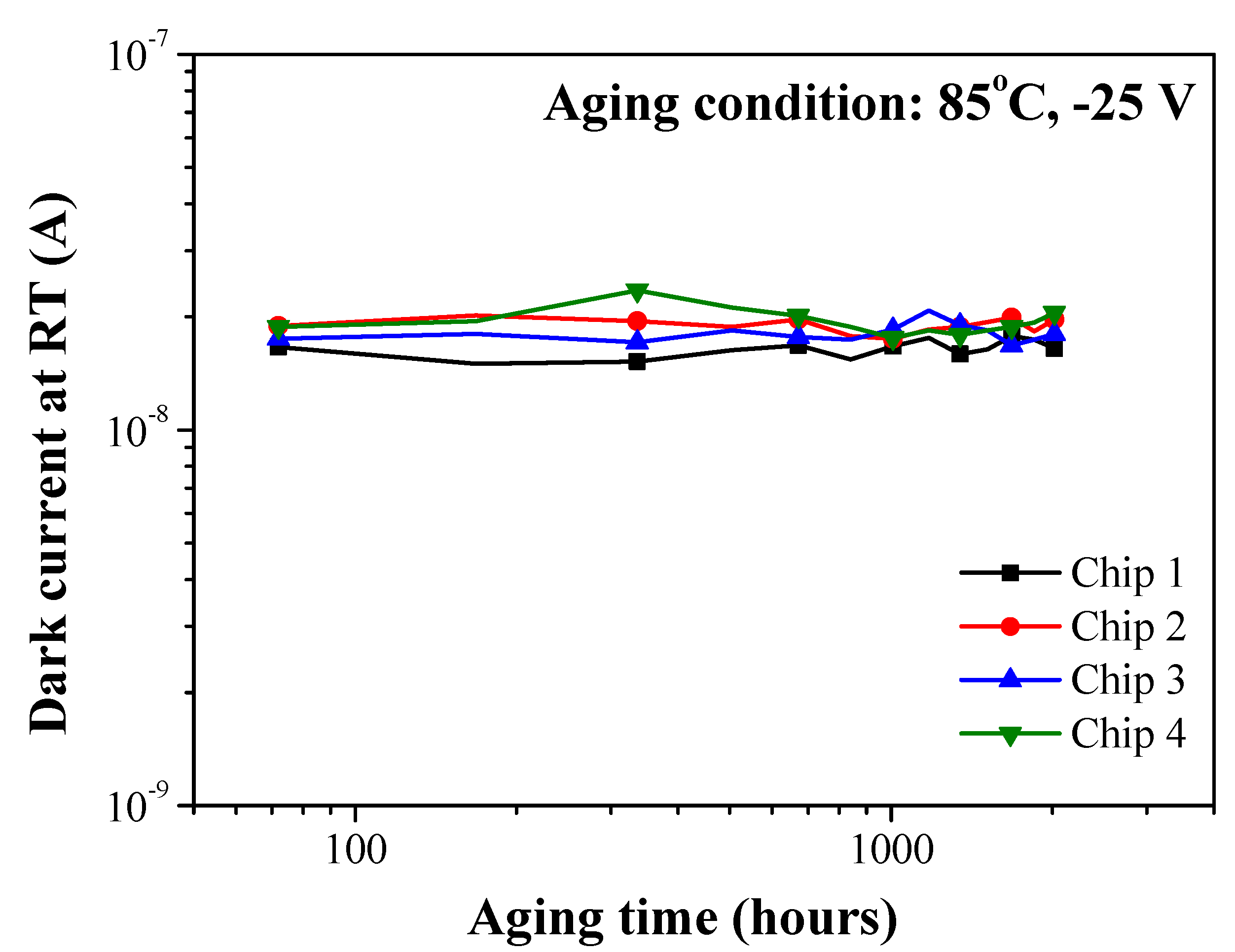
| Aging Time (hours) | Chip 1 ID (nA) | Chip 2 ID (nA) | Chip 3 ID (nA) | Chip 4 ID (nA) |
|---|---|---|---|---|
| 0 | 15.5 | 17.9 | 16.8 | 17.6 |
| 72 | 16.6 | 18.9 | 17.5 | 18.8 |
| 168 | 15.0 | 20.2 | 18.0 | 19.5 |
| 336 | 15.2 | 19.5 | 17.1 | 23.5 |
| 504 | 16.3 | 18.8 | 18.4 | 21.2 |
| 672 | 16.8 | 19.7 | 17.7 | 20.1 |
| 840 | 15.4 | 17.8 | 17.4 | 18.8 |
| 1008 | 16.7 | 17.5 | 18.5 | 17.6 |
| 1176 | 17.6 | 18.5 | 20.8 | 18.4 |
| 1344 | 15.9 | 18.8 | 19.0 | 17.9 |
| 1512 | 16.4 | 19.4 | 18.4 | 18.4 |
| 1680 | 17.8 | 19.9 | 16.8 | 18.8 |
| 1848 | 17.4 | 18.3 | 17.4 | 19.3 |
| 2016 | 16.5 | 19.7 | 18.0 | 20.5 |
| Standard Deviation (S.D.; nA) | 0.8 | 0.8 | 1.0 | 1.6 |
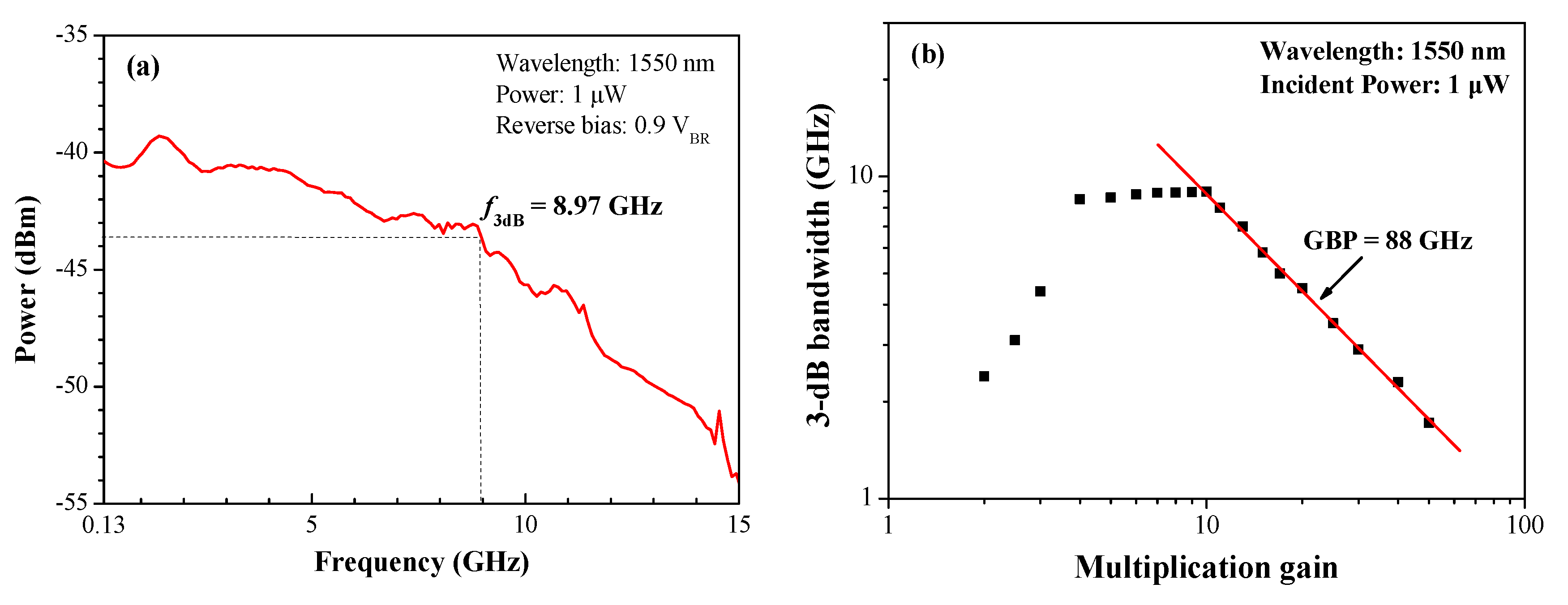
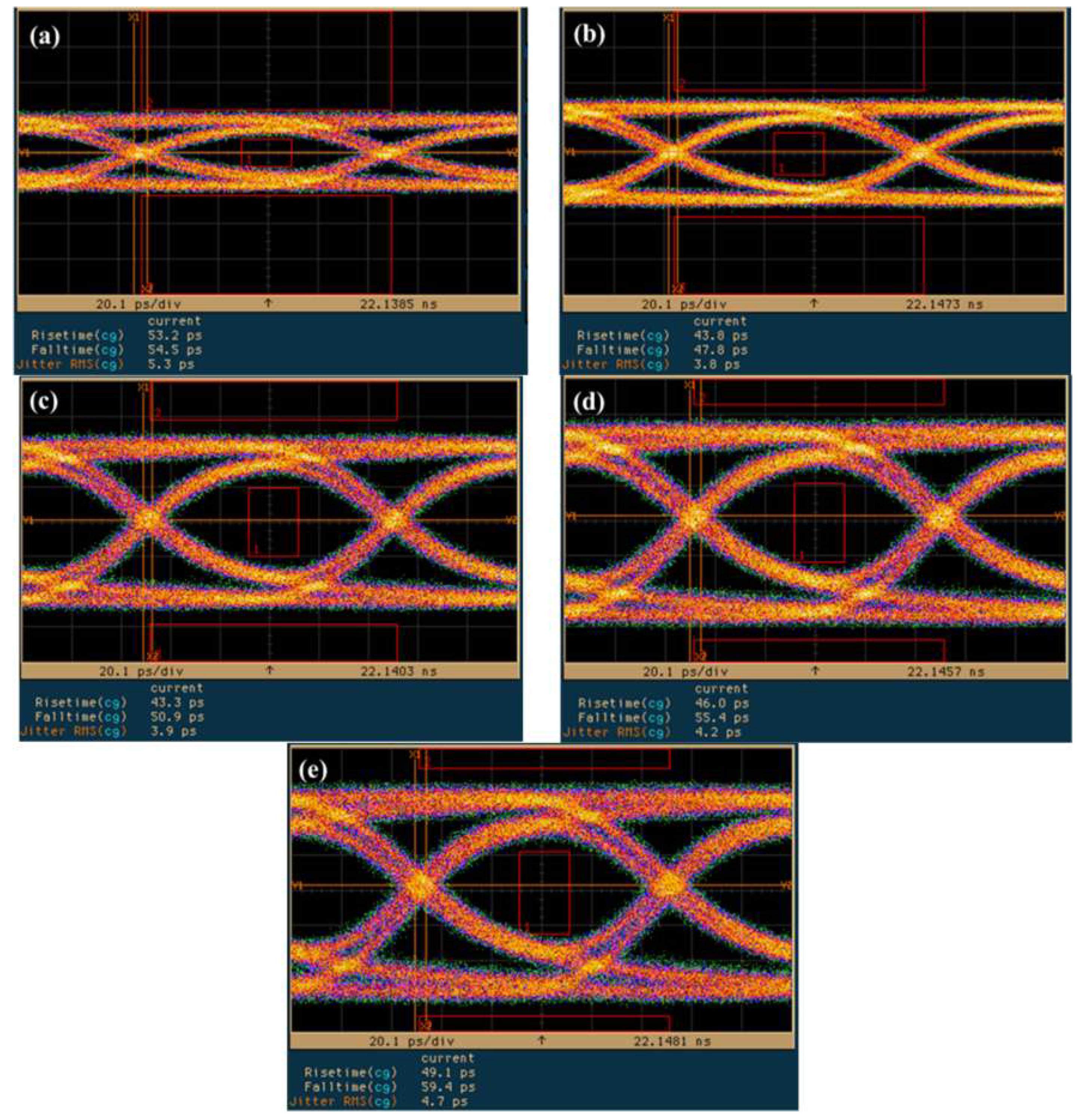
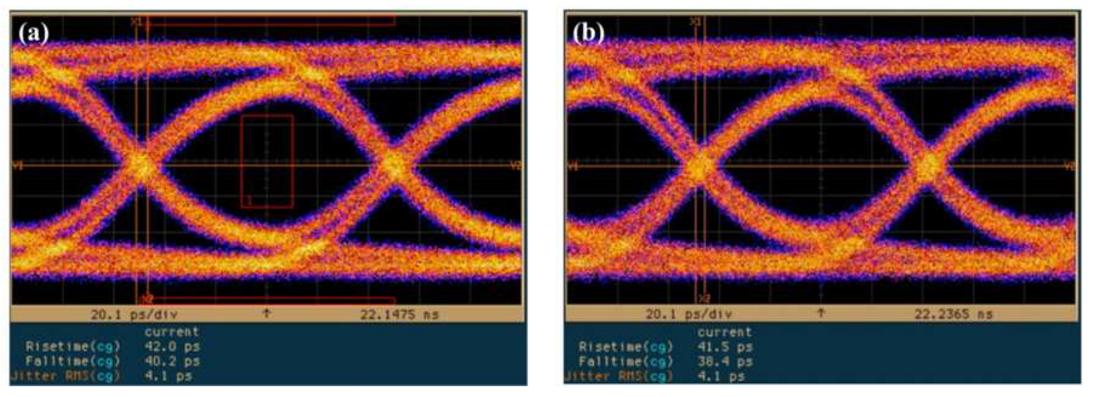
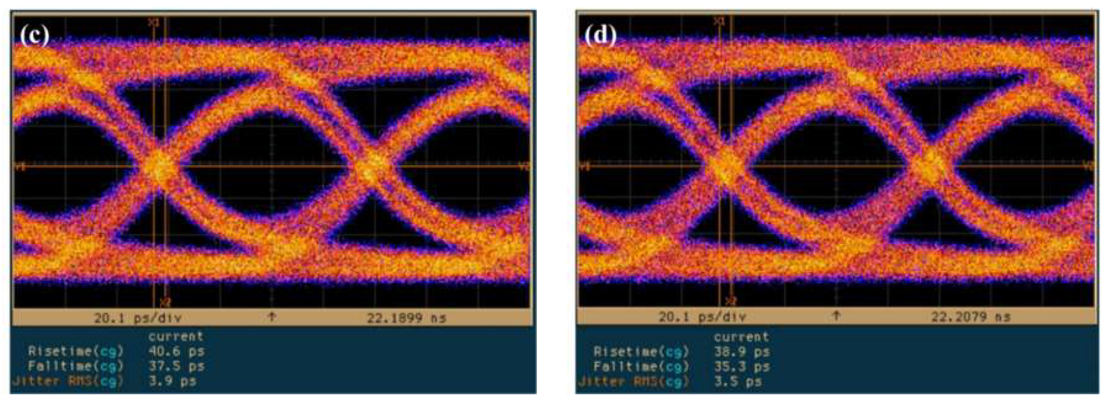
| Speeds @M = 10 | Rise Time (ps) | Calculate f3-dB (GHz) |
|---|---|---|
| Bit rate: 10 Gb/s | 42.0 | 8.33 |
| Bit rate: 11 Gb/s | 41.5 | 8.43 |
| Bit rate: 12 Gb/s | 40.6 | 8.62 |
| Bit rate: 12.5 Gb/s | 38.9 | 8.99 |
| Multiplication Gain @10 Gb/s | -- | -- |
| M = 3 | 53.2 | 6.58 |
| M = 5 | 43.8 | 7.99 |
| M = 10 | 43.3 | 8.08 |
| M = 20 | 46.0 | 7.61 |
| M = 30 | 49.1 | 7.13 |
| Incident power (dBm) @10 Gb/s, M = 10 | -- | -- |
| −17.22 | 50.0 | 7.00 |
| −12.22 | 48.7 | 7.19 |
| −7.22 | 43.3 | 8.08 |
| −2.22 | 35.3 | 9.91 |
| −0.22 | 42.4 | 8.25 |
| 0.78 | 43.3 | 8.08 |
© 2019 by the authors. Licensee MDPI, Basel, Switzerland. This article is an open access article distributed under the terms and conditions of the Creative Commons Attribution (CC BY) license (http://creativecommons.org/licenses/by/4.0/).
Share and Cite
Liu, J.-J.; Ho, W.-J.; Chen, J.-Y.; Lin, J.-N.; Teng, C.-J.; Yu, C.-C.; Li, Y.-C.; Chang, M.-J. The Fabrication and Characterization of InAlAs/InGaAs APDs Based on a Mesa-Structure with Polyimide Passivation. Sensors 2019, 19, 3399. https://doi.org/10.3390/s19153399
Liu J-J, Ho W-J, Chen J-Y, Lin J-N, Teng C-J, Yu C-C, Li Y-C, Chang M-J. The Fabrication and Characterization of InAlAs/InGaAs APDs Based on a Mesa-Structure with Polyimide Passivation. Sensors. 2019; 19(15):3399. https://doi.org/10.3390/s19153399
Chicago/Turabian StyleLiu, Jheng-Jie, Wen-Jeng Ho, June-Yan Chen, Jian-Nan Lin, Chi-Jen Teng, Chia-Chun Yu, Yen-Chu Li, and Ming-Jui Chang. 2019. "The Fabrication and Characterization of InAlAs/InGaAs APDs Based on a Mesa-Structure with Polyimide Passivation" Sensors 19, no. 15: 3399. https://doi.org/10.3390/s19153399