1. Introduction
Commonly used practice for the measurement of soil volumetric water content (VWC) relies on point measurement data for the analysis of water flow dynamics caused by evaporation, transpiration and precipitation, as well as suction from groundwater resources [
1]. Installation of individual sensors at selected depths is destructive to the soil, the cost of the multiple-probe setup together with the necessary accessories (cables, interfaces, data-loggers, etc.) may be substantial, and the installation in the field of a system consisting of many elements is laborious and prone to generate measurement errors caused by possible carelessness during probe installation. Therefore, if the knowledge of VWC at several depths in a soil profile is needed, it is more effective and convenient to use a profile probe in the form of a single tube with sensing elements placed at various distances along the tube [
2]. Such probes usually measure VWC together with soil bulk electrical conductivity (
ECb) and temperature (
T) at different depths of a soil profile. Soil disturbance is minimal and usually the total cost of measurement in three to four soil layers is substantially smaller than is the case with the installation of several separate probes.
Neutron moisture meters (NMM) had been successfully used for the purpose of determining the VWC in the soil profile for nearly 50 years, but radiological regulations and the necessity for constant supervision of the NMM forced soil scientists to use other measurement equipment [
3,
4,
5]. The use of soil electromagnetic (EM) properties gave rise to new sensors and meters of soil VWC. They perfectly fulfill the requirement for automatic and safe measurements. The measurement principle of EM sensors is based on the fact that the presence of water modifies soil complex dielectric permittivity, which in turn modifies the propagation time of EM waves (which is the property used in time-domain sensors), as well as the capacitance/impedance (and oscillation frequency) of a capacitor with soil as the dielectric (which is the property used in frequency-domain sensors). The cost of EM measurement equipment for VWC differs significantly with the measurement frequency range and the measurement accuracy. The GHz frequency sensors do not require soil specific calibration for the majority of mineral soils, while low-frequency sensors (<100 MHz, especially) are susceptible to measurement errors due to electrical conductivity and interfacial polarization effects [
4,
5,
6]. The increasing demand for EM sensors of soil VWC in the global market has resulted in a growing supply in products of various quality, differing in measurement accuracy, calibration methods and measurement volume etc., giving rise to confusion among the users, this demonstrates the need for international testing standards of EM sensors for VWC [
7]. The most important factor in the performance of VWC profile probes is the measurement volume or the sphere of influence. The soil volume measured by the neutron probe is much larger than in the case of any EM probe. Roughly, it is a sphere with a radius from 15 cm for saturated soil to 50 cm for dry soil. Measurements close to the soil surface also have a greater probability of error due to the influence of the soil/air interface [
8]. A smaller measurement volume with EM sensors minimizes the effect of this source of error, however, the effect of the air gap between the access tube and soil caused by possible carelessness during installation or shrinking of the soil can significantly affect the measured VWC values. Moreover, most profile probes have a very small measurement volume, smaller even than individual probes installed at separate depths [
4].
The radius of the sphere of influence depends in general on the sensor design. The maximum possible radius of this sphere can be estimated based on the penetration depth
of the plane wave, which is given as [
9]:
where
and
are the values of the real and imaginary parts of the complex relative dielectric permittivity
of the tested material, respectively,
c is the speed of light in free space and
f is the frequency of the electromagnetic wave. The imaginary part of dielectric permittivity depends on dielectric loss
and bulk electrical conductivity
(dSm
−1), according to the relation
. Therefore, the
value decreases with an increase in frequency and an increase in bulk electrical conductivity of the measured material. The values of the penetration depth of the plane wave may reach an order of meters at frequencies below 100 MHz, and decrease to centimeters above 10 GHz.
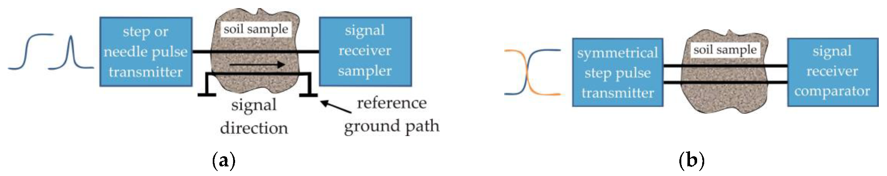
In the paper, an innovative soil moisture profile probe based on the time-domain transmissometry technique (P-TDT probe) is presented. The crucial innovation of the P-TDT probe is the application of digital fast integrated circuits and two symmetrical, opposite phase, electrical step pulses for the generation and measurement of their travel time
along a transmission line placed in soil (see
Figure 1a,b). Analog signal processing of fast step or needle electrical pulses require individually calibrated samplers. The use of symmetrical transmission allows for the improvement of the transmission time measurement accuracy as it is less sensitive to impedance mismatches of the signal paths. The use of symmetrical transmission also reduces the total cost of a single segment of the proposed P-TDT probe due to the application of highly integrated ECL digital circuits. The technical details of this solution are described in the Polish patent No. PAT.228416 [
10].
The objective of the paper is to determine the penetration depth
of the presented P-TDT probe with the use of digital simulations and broadband measurements (10 MHz–10 GHz) using a vector network analyzer (VNA) and a profile probe prototype. A minor part of the research work presented here was published in [
11].
2. Materials and Methods
The digital simulations were performed with the use of the following software tools: (1) 3D electromagnetic wave simulation in the frequency domain for finding the electromagnetic interaction between the probe body and the surrounding material, and (2) electronic design software to convert data collected in the frequency domain to the time domain. This combination of simulations helped to significantly shorten the time to develop a working prototype of the profile probe by optimizing its geometry and measurement circuitry, to identify sources of errors, to test the resolution/accuracy and to minimize the cost of the measurement unit.
Below, the mechanical construction of the prototype P-TDT probe is described. Its geometry was analyzed and optimized using 3D finite element method (FEM) simulations. The geometry chosen for the P-TDT prototype was tested with respect to the penetration depth of the electromagnetic pulse in the dielectric media simulating soil of various moisture content and salinity. The penetration depth of the prototype was verified based on measurements in ethanol, distilled water and sandy soil with two moisture values. All calculations were made using Excel spreadsheet functionality, including nonlinear curve fitting by Solver add-in.
2.1. Construction of the P-TDT Probe
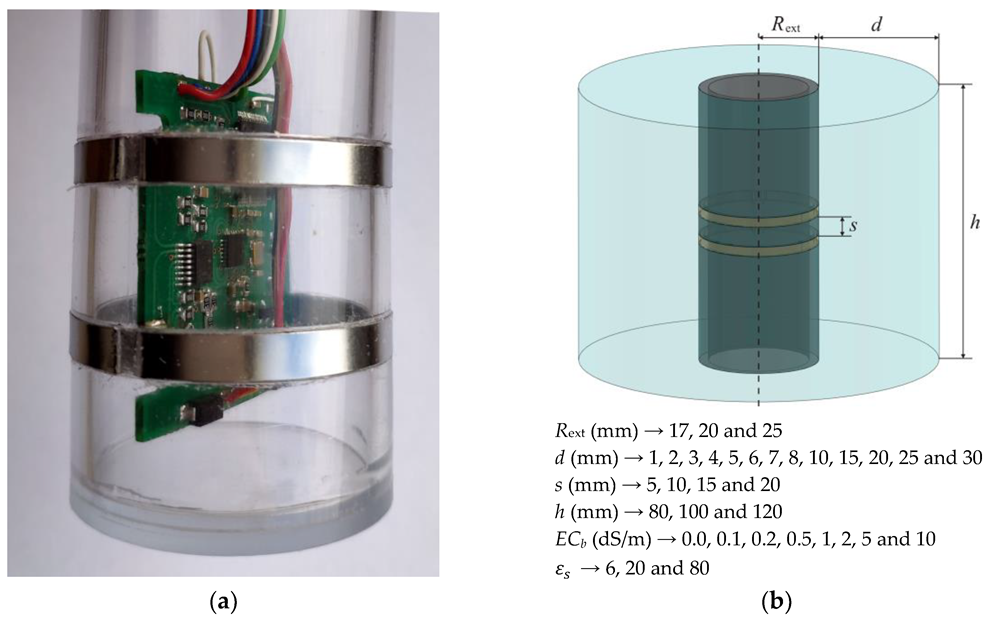
A prototype of a single P-TDT probe section is shown schematically in
Figure 2. It was constructed as a transmission line, which was wound around the plastic body of the P-TDT supporting tube.
The probe was designed to be placed vertically in the soil in a previously drilled pilot hole without an access tube. The entire profile-probe consists of a number of transmission-line sections such as the one shown in
Figure 2a. The number of sections may vary so as to monitor soil moisture, temperature and electrical conductivity at required soil depths.
The electromagnetic field generated by the pulse travelling along a section with the ‘parallel’ transmission line penetrates the soil and the internal part of the PVC tube. The internal part of the probe is watertight and consists of: material forming the body of the probe (preferably not absorbing water from the surroundings, e.g., POM-C [
12]), air, a printed circuit board (PCB) made of epoxy resin type FR4 and electronics. The internal part of the probe presents a stable environment for electromagnetic wave penetration. On the opposite side, the soil placed outside the probe body changes the conditions for fast electrical pulse travel time and attenuation due to the variation of its moisture content, temperature and electrical conductivity.
The physical quantity used to describe electrical properties of the soil from the point of view of the electromagnetic field generated by the propagating electric pulse, is its relative complex dielectric permittivity
. The sensing element consists of two metal strips wound around the probe cylindrical enclosure (
Figure 2a). In the presented design, the sensing element is in direct contact with the soil. Three or more identical sections in the probe are built from parallel transmission lines that are equipped with independent electronic circuits. Each section monitors soil moisture, temperature and electrical conductivity at required soil depths.
Figure 2b shows the shape and dimensions of one section of the digitally modeled probe and its surrounding material.
The electromagnetic field generated by the pulse travelling along the transmission line penetrates the soil and the internal part of the plastic tube. The internal part of the probe consists mainly of the plastic body of the probe, air as well as an electric board (PCB made of epoxy resin type FR4) with electronics that as a whole present a stable environment for electromagnetic wave penetration. Only the soil at the external part of the transmission line causes the electromagnetic field to change with moisture content, temperature and electrical conductivity. Relative complex dielectric permittivity is related to electric pulse travel time t along the transmission line, .
2.2. Digital Simulations
Digital simulations combine the frequency and time domain analysis of a broadband signal travelling along the metallic strips forming the transmission line of the profile probe. Frequency domain analysis was done by means of a three dimensional electromagnetic simulation software pack (Keysight EMPro 3D EM Simulation Software). It determined electromagnetic interaction between the probe’s surrounding material and the body of the probe in the frequency range from 10 MHz to 10 GHz. This interaction is described by the
S scattering matrix, which was calculated using the finite element method (FEM) [
13]. The Port1 (input) and Port2 (output) were placed at the beginning and the end of the two metallic strips respectively. The boundary conditions of the material were fixed as absorptive, thus no reflection from boundaries occurred. The material outside the measured thickness had dielectric parameters of air (
).
Next, the scattering matrix S was imported into the Keysight Advanced Design System software pack (ADS) as an element of the electric circuit so as to convert the frequency domain simulated data into the time domain. The ADS software calculates the propagation time and the attenuation of an electric pulse (narrow symmetrical needle pulse of 1 V amplitude and the half-width of 150 ps) along the waveguide formed from the metallic strips wound around the supporting plastic tube of the profile probe. These values depend on the dielectric permittivity, which is related to the volumetric water content (VWC), bulk electrical conductivity () and volume of the soil material surrounding the profile probe.
The dielectric parameters of the tested material were described by a single-relaxation Debye formula:
where
5.2 and
9.45 × 10
−12 s are values for water,
= 8.85 × 10
−12 Fm
−1, applied frequency
f changed from 10 MHz to 10 GHz with at least 20 points per decade. The parameters that varied were:
Rext (mm)—external radius of the plastic tube with metal strips of the probe’s transmission line,
d (mm)—thickness of the probe’s surrounding material,
(dSm
−1) and
—its electrical conductivity and low frequency dielectric permittivity respectively,
s (mm)—distance between two metal strips of the probe’s parallel transmission lines and
h (mm)—height of the profile probe section. The width and thickness of metal strips were fixed to 5 mm and 0.3 mm respectively.
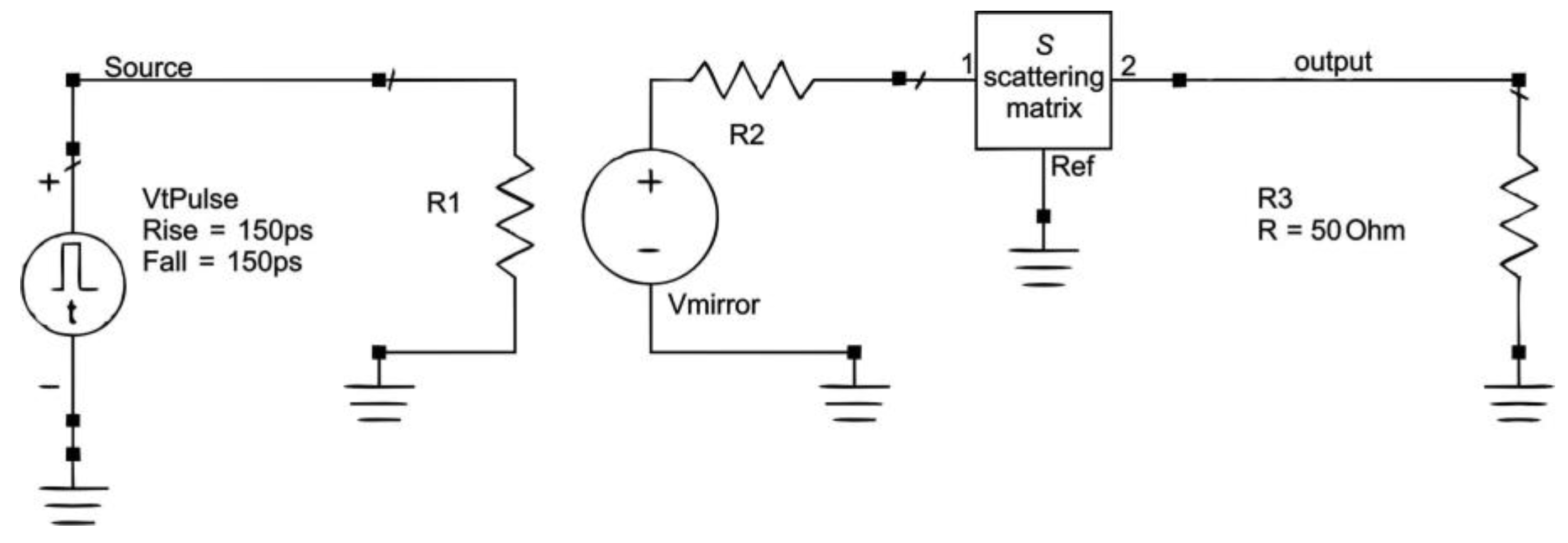
The elementary electric circuit used in ADS is presented in
Figure 3. The VtPulse element is a needle pulse generator of 150 ps rise and fall times and 1 V amplitude, the R1 = R2 = R3 = 50 ohm, Vmirror serves as the controlled voltage source,
S is the scattering matrix imported from EMPro for the given geometry and external material of the profile probe. In total, several thousand FEM digital simulations were done for many combinations of
Rext,
d,
s,
h,
ECb and
(see
Figure 2b). The use of the R1, R2 and Vmirror setup in the circuit enabled connection to the source VtPulse in parallel so as to quickly obtain several waveforms representing various combinations of the
d parameter when the others were fixed.
2.3. VNA Measurements
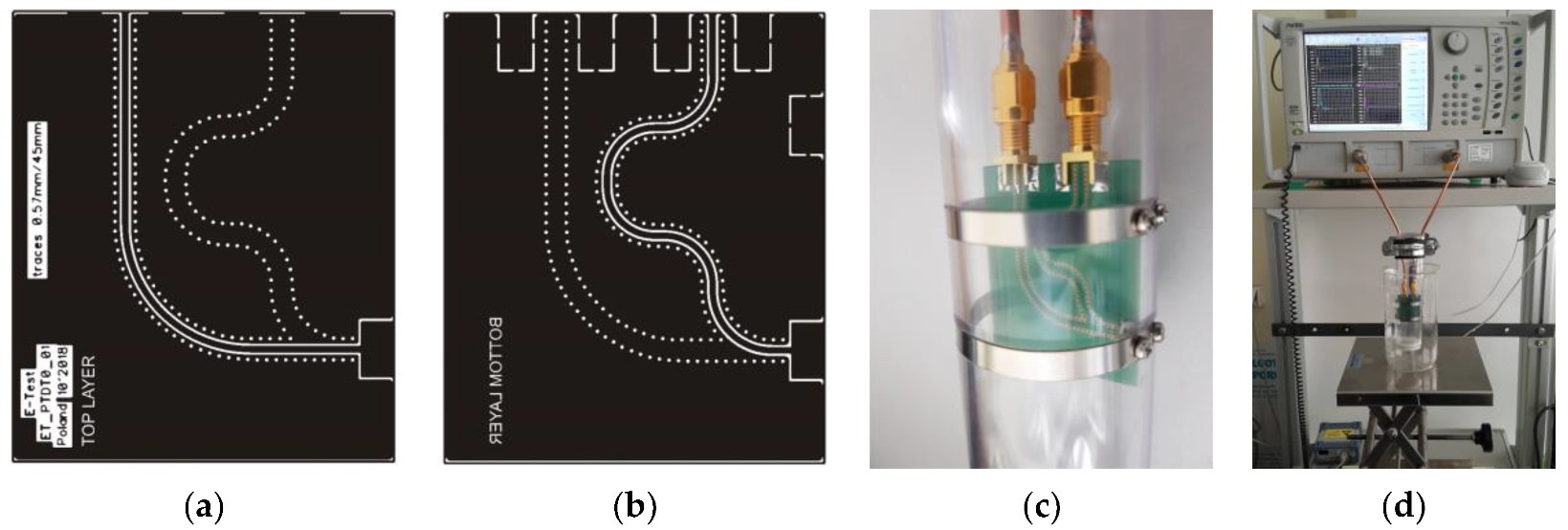
Verification of the profile probe performance obtained from digital simulations was done on the prototype construction presented in
Figure 4. The two internal layers of the FR4 four layer printed circuit board (PCB) were connected to the ground by means of via pads. The thickness of the top and bottom layer was the same, and together with the top and bottom paths they formed 50-ohm transmission lines of the same length (
Figure 4a,b). The lower metallic strip of the profile probe was connected to VNA port 1 by means of the transmission line on the bottom side of the PCB, and the other end of the lower strip was connected to VNA port 2 using the transmission line on the top side of the PCB. Both transmission lines were connected to the VNA ports by SMA edge female connectors and semi-rigid cables about 20 cm long (
Figure 4c,d). The upper metallic strip of the profile probe was connected to the ground layer on both sides. The bottom part of the plastic tube supporting the metallic strips was tightly sealed. In this way the VNA transmission measurements were possible in materials surrounding the strips from outside. Metallic strips were made of stainless steel (width 5 mm, thickness 0.3 mm), the distance between them was
s = 16 mm, the external and internal radius of the plastic tube were 20 mm and 17 mm respectively. The strips were connected to the PCB with screws.
The VNA (2-port Anritsu VectorStar MS4642A, bandwidth 70 kHz–20 GHz) measurements were made in a constant temperature 20 ± 0.5 °C in laboratory conditions. Before measurements the VNA was turned on for about one hour to stabilize its temperature, both ports were calibrated following the respective instructions supplied by the producer of the device. The full scattering matrix S in the frequency range 10 MHz–10 GHz was collected for each measurement. Next, the measured S parameters were imported to the Keysight ASD program for further processing in a similar way as described earlier.
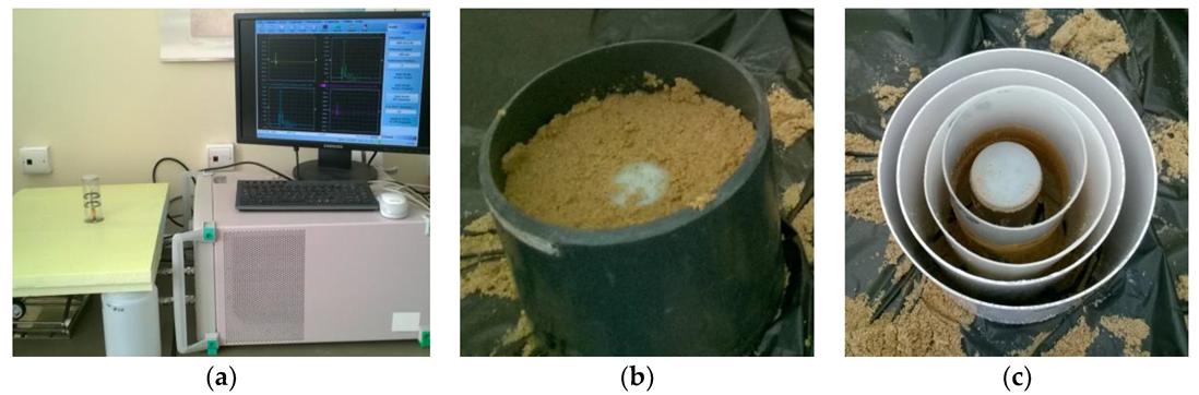
The P-TDT prototype probe was placed centrally in cylindrical containers of 50 mm, 56 mm, 66 mm, 86 mm and 103 mm diameter, which were filled with deionized water and ethanol (purity 96%). The cylinders were filled with liquids to have a distance of at least 27 mm between the metallic strips and the top/bottom of the liquid in the cylinders.
A similar experiment with sandy soil was performed. Dielectric response of moistened soil may change depending on soil compression, thus the experimental setup was slightly modified (
Figure 5) in comparison to the previous experiment with liquids in order to eliminate that error. The intention was to measure the same soil sample with the same density but with different thicknesses around the P-TDT probe.
One section of the P-TDT probe was mounted upside down in an extruded polystyrene (XPS) plate (
Figure 5a) and a thin-walled pipe with 146 mm in diameter was located on the plate coaxially with the probe. The space between the pipe and the probe was filled with wet soil before performing measurements. A smaller pipe 125 mm in diameter was put into the soil coaxially with the probe (
Figure 5b), then the soil outside and the bigger pipe were removed before the next measurement. The procedure was repeated six times for the pipes of 100 mm, 82 mm, 65 mm and 46 mm in diameter (
Figure 5c). This method ensured measurements of the practically intact soil sample with differences between dielectric responses from each measurement resulting only from various soil-layer thickness around the P-TDT probe.
3. Results and Discussion
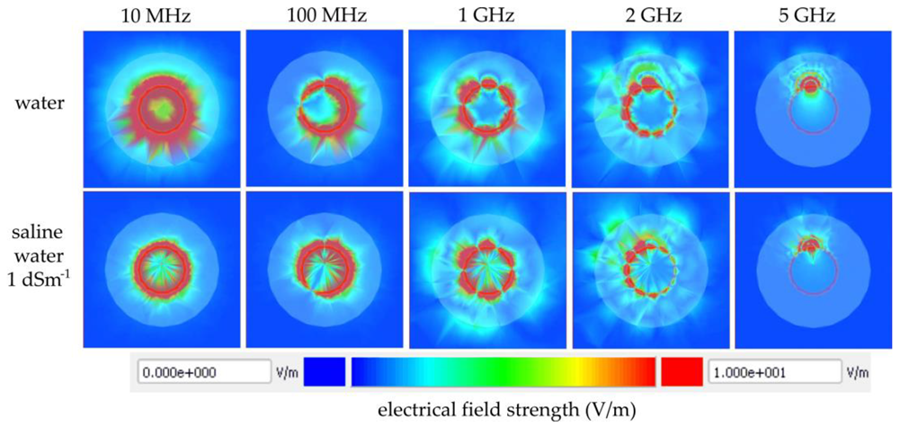
Distribution of the electromagnetic field around one section of the P-TDT probe placed in distilled water and in a KCl water solution of 1 dSm
−1 electrical conductivity in relation to the frequency of the applied signal is presented in
Figure 6. These pictures are screenshots from the animation utility of the Keysight EMPro 3D electrical FEM simulations of one section of the P-TDT probe geometry from
Figure 2b. Increasing the applied electrical-field frequency resulted in reduction of the penetration depth and also created resonances around the metallic strips of the probe. Above 2 GHz the strength of the electric field was continuously decreasing with frequency, and at 5 GHz the pulse could not reach the end of the P-TDT transmission line. Furthermore, the electrical conductivity of the medium limits the penetration depth of the electrical field, especially at frequencies below 100 MHz. With a frequency increase above 100 MHz there was almost no difference in the electrical field distribution in the distilled water and saline water.
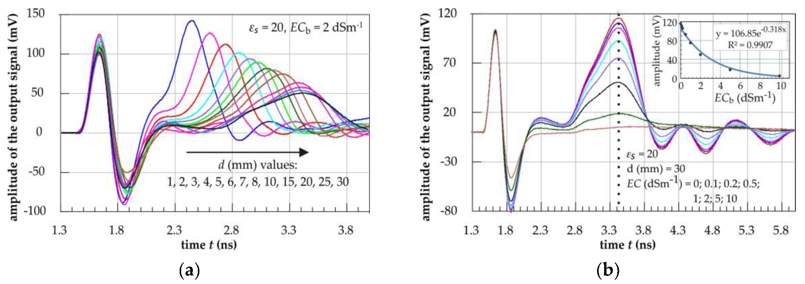
The output waveforms from the ADS digital simulator for various thicknesses
d of the measured material with fixed values of
= 20,
= 2 dSm
−1,
h = 80 mm and
s = 15 mm are presented in
Figure 7a. The first positive and negative amplitude in
Figure 7a,b represents a crosstalk of the initial 1 V amplitude needle pulse from the VtPulse element between input and output of the transmission line. It was caused by a capacitive coupling and may be used as the time marker to start the measurement of the propagation time of the pulse along the metallic strips of the transmission line. The increase of the material thickness
d resulted in increasing the transmission time
t of the applied pulse, but not in the same proportion (
Figure 7a). The second positive pulse of the waveforms represents the output of the P-TDT transmission line for the material thickness equal to 1 mm, 2 mm, … and 30 mm. However, the increase of
t was faster for smaller values of
d. Furthermore, the amplitude of waveforms decreased as the material thickness increased. This is what was expected. Similar figures can be drawn for other combinations of
,
d and
.
Increase of
for fixed values of
and
d resulted in an exponential decrease of the transmitted signal amplitude, as seen in the inlet graph in
Figure 7b. The propagation time
t of the pulse did not change with the increase of the material
, which is marked as the dotted line in
Figure 7b. Above
= 5 dSm
−1 the transmitted signal was almost completely attenuated and it was not possible to determine the transmission time
t.
It was proposed to model the change of the propagation time
t of the pulse along the profile probe’s transmission line with the increase of material thickness
d with the following exponential limit formula:
where
b (ns) is the value of
t for
d = 0 mm,
A (ns) stands for the maximum increase of
t for
d reaching infinity and
k (mm
−1) is a shape factor related to the
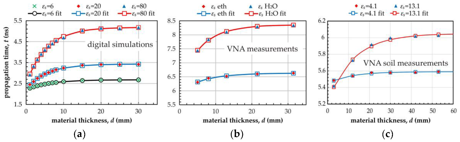
t rise. The dependency of
t on
d given in Formula (3) was presented in
Figure 8a for the digital simulation data, in
Figure 8b for the VNA measurements data collected from the P-TDT prototype inserted centrally into plastic containers filled with water and ethanol and in
Figure 8c for sandy soil measurements.
3.1. Results from Digital Simulations
Digital simulations were conducted for three materials with static values of the relative dielectric permittivity
equal to 6, 20 and 80 respectively, when material thickness
d changed from 1 to 30 mm in steps from 1 to 5. Fitted lines follow Formula (3) with parameters given in
Table 1. A new parameter
d99% was defined as the material thickness critical value for which the travel time
t along the metallic strips of the P-TDT probe reaches the value of
and consequently
. Thus, it can be easily calculated that
. The
d99% parameter gives an approximation of the electromagnetic wave penetration-depth calculated from digital simulations or VNA measurements. The summarized results of digital simulations for selected geometries of the tested probe for three values of
equal to 6, 20 and 80 were shown in
Table 1.
The measured material volume was a cylindrical shell with the internal inner radius
Rext equal to the radius of the P-TDT supporting tube and
d99% thickness. The average value of
d99% calculated from digital simulations for three tested materials with the values of the static dielectric permittivity
equal to 6, 20 and 80 was
d99%_ave = 26.05 ± 1.40 (standard deviation of the sample mean) for the chosen geometry marked in bold in
Table 1. It can also be seen that the smaller the distance between the strips, the smaller is the penetration depth. The value of
d99% for the distance between metallic strips
s = 5 mm was significantly smaller than for longer distances, which were tested. It seems that the geometry
Rext = 20 mm,
s = 15 mm was a reasonable choice for building the P-TDT prototype probe.
Since no change of the transmission time
t was observed for various values of
for a fixed value of
d (see
Figure 7b), the parameters
A and
k in Formula (3) apply for all values of
in the analyzed range of variability from 0 to 10 dSm
−1. Therefore, it was concluded that the penetration depth
d99% determined from the digital simulations did not depend on the bulk electrical conductivity
of the material surrounding the P-TDT probe.
An important issue in the presented calculations was the measurement range of the transmission time t described by parameter A, which refers to the infinite value of d. The value of A changes from 0.47 ns for = 6 (dry soil) to 2.69 ns for = 80 (water). So, the propagation time t measurement with a sufficient resolution in this time range, for example 1000 points in a linear time scale, gives about 2 ps spacing between two measurement points, which is an engineering challenge.
3.2. VNA Measurements on the P-TDT Prototype
The prototype P-TDT probe geometry was chosen on the basis of the digital simulation results (
Rext = 20 mm,
s = 15 mm). Verification of the digital simulation for this construction was done with ethanol, distilled water and sandy soil as measurement media, and plastic containers and tubes with various diameters. The output waveforms in the time-domain that were generated by ADS electrical simulator on the base of the
S scattering matrix measured by VNA, are presented in
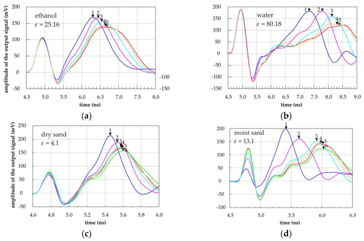
Figure 9. Similar waveforms could be produced directly by the VNA equipped with a time-domain conversion option. The filled triangles are markers showing the values of propagation time
t, which are further processed to obtain the
d99% parameter as the P-TDT penetration depth indicator. The waveforms in
Figure 7, where the scattering matrix
S was determined with FEM 3D simulations, and the waveforms in
Figure 9a–d, where
S was measured by VNA connected to the prototype P-TDT probe, are very similar. The first pulse result from the signal crosstalk by the capacitive coupling between the beginning and the ending of the transmission line made of metallic strips. The other positive pulses on the waveform indicate the discontinuity of impedances between the transmission line on the surface of the P-TDT probe and the planar 50 ohm transmission line on the printed circuit board. Similarly to the digital simulations, the bigger diameter
d of the container filled with ethanol, water or soil, the longer is the travel time
t of the pulse along the P-TDT transmission line.
The graphical relation between travel time
t and material thickness
d for the prototype P-TDT probe is shown in
Figure 8b,c. The parameters of the fitted exponential limit curve (3) are presented in
Table 2.
The penetration depth (or the measured effective thickness)
d99% of the dielectric material measured by the P-TDT probe was bigger than the values received from digital simulations. Comparing the value of this parameter from the measured data on ethanol and water with the simulated data for the value of
= 20 and 80, we saw a 24% and 9% increase respectively. This effect can be explained by the possible errors in reading the travel time t from the waveforms in the time domain generated by the ADS electronic circuits simulation software for the measured data, especially for large diameter values of the containers with water (see
Figure 9b). The penetration depth calculated from Formula (3) for sandy soil was 49.08 mm and 55.36 mm for dry and moist sand respectively. However, measurement data from
Figure 8c showed that good enough measurement results for dry soil could be obtained even for a 20 mm thick sample and 30 mm for moist soil. Care should be taken to design and manufacture the interfaces between the successive elements along the fast pulse signal travel path to avoid signal reflections and distortions. They could significantly increase measurement error.
4. Conclusions
The combination of 3D FEM digital simulations for geometry of the P-TDT sensor has been presented. The simulations in frequency and time domain were performed. The S scattering matrix obtained from frequency domain described the interaction of a sensor with the surrounding material. Moreover, the S matrix was used in time domain simulations of the final electrical circuit of the sensor. The presented combination of 3D FEM digital simulations can significantly shorten the time for developing a working sensor prototype. This is especially useful for sensors working in the microwave frequency range, where mechanical imperfections introduce signal distortion.
The penetration depth evaluated by the digital simulations and verified by VNA measurements on the prototype P-TDT probe appeared to be sufficient for the practical applications for soil moisture measurements in the frequency range comparable to the commonly used TDR technique. The material thickness measured by the analyzed soil moisture profile probe, as defined by the d99% indicator, was in the range of 20–30 mm. It did not depend on soil electrical conductivity in the range up to 5 dSm−1, which corresponds to the commonly accepted soil bulk electrical conductivity upper limit for plant growth.
The transmitted signal amplitude corresponded to the soil bulk electrical conductivity, which enabled simultaneous measurements of soil moisture and salinity from the same soil volume. The addition of a temperature sensor in close proximity to the metallic strips of the P-TDT section would also be necessary to make temperature corrections of the measured electric pulse time propagation. This propagation time enables soil moisture to be calculated, but it depends on dielectric permittivity, which in turn depends on temperature. It might be problematic to measure very short time distances in the time scale of the fractions of a nanosecond with an acceptable resolution and accuracy, which could affect the VWC measurement accuracy of dry soil. Future work on the electronic hardware and software will address these issues with short time distances.
In this paper, the initial part of the research on the P-TDT probes was presented. It is expected that the final product will be an economic and durable field measurement device for monitoring the dynamics of soil moisture, electrical conductivity and temperature at various soil layers. The performance of the final construction of the P-TDT probe, including the applied electronic solutions, is to be the subject of a future paper.

 ,
, 


