Energy/Area-Efficient Scalar Multiplication with Binary Edwards Curves for the IoT


1
CINVESTAV Tamaulipas, Victoria 87130, Mexico
2
CINVESTAV Guadalajara, Zapopan 45019, Mexico
*
Author to whom correspondence should be addressed.
†
These authors contributed equally to this work.
Sensors 2019, 19(3), 720; https://doi.org/10.3390/s19030720
Submission received: 30 November 2018
/
Revised: 29 January 2019
/
Accepted: 30 January 2019
/
Published: 10 February 2019
(This article belongs to the Special Issue Privacy and Security for Resource Constrained IoT Devices and Networks)
Abstract
:Making Elliptic Curve Cryptography (ECC) available for the Internet of Things (IoT) and related technologies is a recent topic of interest. Modern IoT applications transfer sensitive information which needs to be protected. This is a difficult task due to the processing power and memory availability constraints of the physical devices. ECC mainly relies on scalar multiplication (kP)—which is an operation-intensive procedure. The broad majority of kP proposals in the literature focus on performance improvements and often overlook the energy footprint of the solution. Some IoT technologies—Wireless Sensor Networks (WSN) in particular—are critically sensitive in that regard. In this paper we explore energy-oriented improvements applied to a low-area scalar multiplication architecture for Binary Edwards Curves (BEC)—selected given their efficiency. The design and implementation costs for each of these energy-oriented techniques—in hardware—are reported. We propose an evaluation method for measuring the effectiveness of these optimizations. Under this novel approach, the energy-reducing techniques explored in this work contribute to achieving the scalar multiplication architecture with the most efficient area/energy trade-offs in the literature, to the best of our knowledge.
1. Introduction
The deployment of Internet of Things (IoT) applications is pushing society to interact with smart environments on a regular basis. Smartphones, buildings, vehicles, roads, home appliances; most new instances of these technologies are being equipped with capabilities for data sensing and internet connectivity [1]. The data retrieved by these systems might be sensitive, since it can be inherently confidential [2] or can be used to infer a user’s behavior [3]. Providing security for the IoT is said to be the equivalent of providing security for a conventional network, with the added complexity that the network can be physically reached by attackers [4].
A common characteristic in many IoT nodes is that they suffer from physical constraints, most notably on size and energy [4,5]. For reducing manufacturing costs, devices’ physical size needs to be decreased.
For some, one of the most precious resources of a constrained device is energy [6,7]. The reasoning is that after deployment, some nodes rely on battery systems which cannot be replaced and ought to last for several months or years. That is why “to minimize energy consumption, lightweight Public-key Cryptography (PKC) implementations are a fundamental requirement” [8]. For both cases, lightweight cryptography can provide an effective solution that (a) is physically small and (b) has low energy consumption.
Elliptic Curve Cryptography (ECC) has proven to be one of the best PKC alternatives for constrained applications [8,9,10,11,12,13] where multiple restrictions are also observed. Compared to other PKC systems, ECC features reduced key sizes for equivalent security levels [14]. ECC can be used for achieving key establishment, encryption, authentication, and signatures, among other security functions. The fundamental operation required in ECC is kP—which relies on a huge amount of field operations. Although improving the performance and area of this algorithm has been widely addressed in the literature, the energy profile of these systems has been seldom studied [15].
The most popular strategy for reducing the energy consumption of an implementation is to reduce its runtime [16,17,18,19,20]. However, some performance-enhancing techniques might prove to be too costly for constrained devices in terms of hardware utilization. Area minimization can also lead to energy savings by reducing the power dissipation—to a lesser extent this approach has also been studied in the literature [21,22]. Experimenting with the tradeoffs of both methodologies can lead to novel design insights which can be used to reduce the energy footprint of the system.
In this paper, we explore the area/energy tradeoffs on a FPGA-based realization of the multiplication scalar for Binary Edwards Curves (BECs) [23]. We use a lightweight area-oriented kP architecture as the starting point for applying a sequence of energy-related improvements. The efficiency of these modifications is assessed at each step. Our approach emulates an incremental development, where in the final step a solution which is efficient in both hardware usage and energy consumption is obtained. We have chosen BECs as case study, but the energy-reduction strategies applied can be translated to any other elliptic curves. Our optimizations focus on hardware since in that way the module can be used as a security accelerator which is enabled upon request to further save energy. The proposed improvements are evaluated with performance and area metrics, as well as with a novel method for estimating the energy savings in relation to area costs. Under this novel approach, we show that one of the kP architectures proposed—to the best of our knowledge—is the most efficient design reported. As evaluation platform we use the xc6slx16 low-cost FPGA operating at commonly used frequencies.
Our contributions can be summarized as follows:
- The detailed implementation and assessment of energy-reducing techniques are presented. The techniques employed are often used in the literature, but the actual effectiveness of each one is seldom explored. In this paper we aim at filling this gap by providing detailed implementation results. With this study, researchers aiming at producing new low-energy designs can have a precedent for choosing the strategies best suited to their projects.
- Our architectures improve the state of the art in regards to area/energy efficiency. This is in part thanks to the carefully designed cryptosystem, and to the followed design methodology.
- We have created and described a novel evaluation metric for assessing the efficiency of the proposed architectures in terms of energy reduction and area increments. This metric can account for variations in the measurement units, the operational frequency, and the underlying finite field. Thanks to these points we were able to employ the novel metric for benchmarking our architectures and the entirety of the state of the art for low-power/low-energy scalar multiplication realizations.
The rest of the paper is structured as follows. Section 2 briefly enumerates some preliminary notions regarding the topics in this paper. Section 3 describes the energy-oriented improvements applied to ECC architectures in selected works from the literature. The description and implementation for our energy improvements can be found in Section 4. A novel evaluation method for energy improvements is detailed in Section 5. Lastly, our concluding remarks are available in Section 6.
2. Preliminaries
2.1. Elliptic Curve Cryptography
An elliptic curve can be described as the set of points that satisfy the Weierstrass model in (1) over the finite field .
Simplifications of (1) and equivalences are used as the basis for different elliptic curve families: random prime, random binary, Koblitz, Montgomery, Edwards, twisted Edwards, binary Edwards, among others.
The elliptic curve points E, a group operation + and the point at infinity form an elliptic curve group E(), which can be used in cryptographic applications. The operation + is the addition of points, it varies for each elliptic curve family. Thus kP represents the consecutive application of the group operation k times over the base point or generator P:
In practice kP relies on point addition () and doubling (), where each is composed of multiple field operations. The complexity of kP depends on the group and field arithmetic definitions. The kP calculation is used in any ECC-based algorithm, hence improving its efficiency is critical.
The BECs family is defined by the model
where with and . These curves are birationally equivalent to binary generic curves [23]. Their principal advantages of BECs are that (a) their group operation is complete, so no extra checks are required and (b) their group operation requires less field operations.
In [23] the authors introduced the concept of w coordinates for BEC. By using this point representation it is possible to reduce the amount of field operations required in performing kP. Furthermore, the use of projective-w coordinates enables reducing the number of inversions required—inversions are some of the most expensive field operations. Differential addition and doubling formulae can be combined with projective-w coordinates to achieve the smallest requirements in terms of field operations for kP in BECs [24].
2.2. Power and Energy
Let the energy (ENE) consumed by a circuit to perform a task as the product between the dissipated power (POW) and the runtime (t):
We consider the runtime to be directly linked with the performance of the system: lower runtime equals higher performance and vice versa. The runtime is the product of the latency clock cycles (LAT) and the inverse of the operational frequency (f):
POW is obtained as the sum of the dynamic (DP) and static or quiescent (SP) powers:
DP is the sum of powers associated with clocking, signals, logic, IOs, and dedicated blocks; this includes the data-dependent power. SP is dissipated by the whole FPGA fabric and remains somewhat constant regardless of the implemented circuit. For FPGAs the static power tends to be higher than the dynamic part. Each component is usually modeled as
where e is the average energy spent during one clock cycle per area unit, A represents the area of the circuit, is the static current consumed from the power supply, and is the supply voltage. The designer has control over the operational frequency, the latency, and the area to influence the energy consumption of the system.
The effects of f over ENE are not straightforward. If f is reduced, then t grows and ENE rises—as shown in (4)—from the SP component in POW; if f is increased, then POW may grow due its DP element—see (7)—and the increment of ENE follows from (4). Finding the optimal operational frequency for the proposed kP architecture is outside of the scope of this work, we do however use two operational frequencies (low vs. high) to study this variation.
So, if we seek to reduce ENE we need to find a minimum in the balance between the area and the latency. The former has been the main optimization goal for lightweight cryptography, whereas the latter has generated interest in recent years [28].
Other popular optimizations such as clock gating and datapath insulation aim at mitigating the switching activity of parts of the circuit which are not actively used—these aim at reducing the dynamic power consumption of the circuit.
2.3. Percentile Differences
The percentile increment (%) is provided whenever new implementation results are presented. These increments are calculated as the difference between the new () and the previous observation (), with reference to :
In this work we only use percentile differences to assess the area increments and the energy decrements.
2.4. Evaluation Environment
We used the Xilinx ISE Design Suite 14.3 for synthesis and configuration of all the architectures described. The designs were described in VHDL and synthesized with Area Reduction as design goal and strategy2 as strategy. All the results provided in this document were obtained after Place and Route (PAR) unless explicitly stated otherwise.
The power estimations reported in this paper correspond to the sum of dynamic and static power. Since for FPGAs the static part tends to outweigh the dynamic power, in some cases the total power might appear somewhat constant.
These estimations were obtained using the Xilinx XPower Analyzer software. In order to obtain a high overall confidence level we employed the post-PAR design file (ncd), the physical constraints file (pcf) for the specified FPGA, and a simulation activity file (saif). The latter was obtained using the Xilinx Isim software from a post-PAR simulation; each one of the architectures was simulated using actual data for over 10,000 cycles.
3. Energy Reduction in the Literature
Improving the performance of the system is one of the most common approaches for reducing the energy consumption [16,17,18,19,20,29,30,31,32,33,34]. In [35] it is shown that techniques like pipelining and parallelism can be used to reduce the power consumption. If the computations are completed quickly, a moderate rise in the power required (due to increments in the area and switching activity) can be mitigated by the time reduction. In this regard multiple alternatives have been proposed: using low-latency algorithms, proposing low-latency implementations, exploiting algorithm parallelism, and using dedicated processing units. Nonetheless, just as it is inadequate to say that low-area equals lightweight, it is also flawed to assume that high-performance equals low-energy. As reviewed in the previous section, the relations between energy and performance are not clear-cut. The other strategies for achieving power reduction consider area minimization [21,22] and exploring area/performance tradeoffs [32,36].
From the perspective of security protocols, it can be concluded that low overheads in the number of packets [22,37,38,39,40] and the number of cryptographic operations [32,38,41,42,43] are key for low-energy PKC. These nodes are characterized by wireless transmissions, which require considerable amounts of energy to be performed, thus it is opportune to use protocols with low packet count requirements. As mentioned, ECC offers the smallest key sizes for comparable security levels. That property holds for all the group elements, thus contributing to reducing the transmissions overhead.
The implementation platform plays a significant role in the design of an ECC system. Using a generic processor would imply selecting prime curves, since commercial ALUs seldom include binary multipliers. On the other hand, a hardware solution would benefit from using binary curves [17].
Selecting the adequate coordinate representation, the group operations, and the field operations used in the ECC system is of paramount importance. For a software-implementation these choices translate into different routines that are executed by the processor, whilst for a hardware-realization these translate into different hardware modules. Processors benefit from shorter routines, from quick calculations, but also from reduced memory accesses [44]. On the other hand, hardware architectures can exploit the arithmetic of binary fields for performing calculations swiftly.
For hardware systems, low latency designs are generally preferred, although implementing faster application-specific modules can result in expensive area investments. How much hardware can be used for improving performance? In the literature, significant interest has been put into concrete points: (a) selecting the optimal field inverter [16,17,18,19,27,30,41,45,46]; (b) determining the adequate digit size for the digit multiplier [17,22,27,38]; (c) designing dedicated squaring modules [16,17,18,25,27,41,45,47].
4. Methods
In this section we outline the application and evaluation of different energy-reducing techniques over a low-area kP architecture. Throughout the document we use the Binary Edwards Curve BE251 [23] as case study.
We study three architecture-level transformations—field inverter, field multiplier, field squarer—as well as a circuit-level modification—datapath insulation. We study these strategies in the aforementioned order so that the contribution of each technique can be studied in a way in which it benefits the most from previous techniques.
4.1. Starting Point: Low-Area kP Architecture
In Figure 1 we illustrate the base area-optimized architecture used. This module follows the Montgomery Ladder algorithm with differential addition and doubling for binary Edwards curves in mixed-w coordinates as proposed in [24]. One of the main characteristics of this design is that it offers flexibility of the field, curve, base point, and scalar; all the proposed optimizations ought to preserve this property.
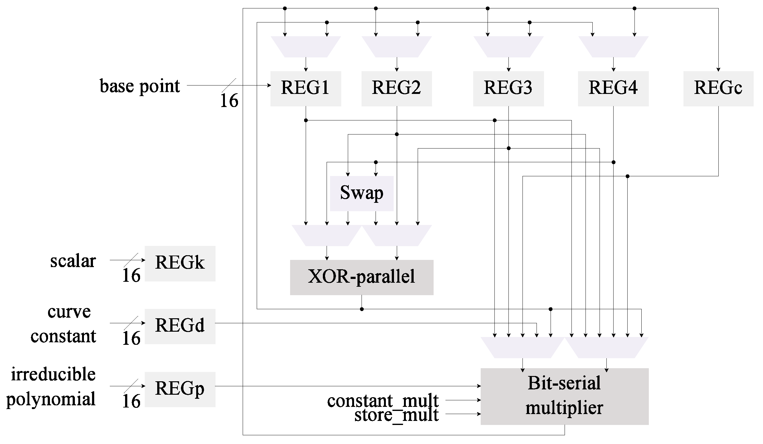
The field operations supported by this design are multiplication, addition, and inversion. A bit-serial like multiplier is used to reduce implementation size. Addition is performed by a layer of XOR gates. Field inversion is required to convert the input and output of the system from w to projective-w coordinates and vice versa. This operation is performed with only multiplications thanks to Fermat’s Little Theorem. The particular inversion algorithm used is Wang’s [51].
In regards to latency, each inversion requires m-bit multiplications, which amounts to 125,249 cycles when . A step in the Montgomery ladder requires full multiplications with a latency of 567,009 cycles, m short multiplications with a latency of 14,558 cycles, and additions which take 753 cycles. The architecture requires two inversions and an m-bit Montgomery ladder per kP, hence the total latency of the design is 832,818 cycles.
While this design performs well in regards to hardware resources, it requires many latency cycles. This has a negative effect on the performance and energy consumption of the system. In the following we review the application of different optimization strategies devised to reduce the energy footprint.
4.2. Modification 1: Inversion Algorithm
Field inversion provides a convenient way to perform divisions in finite fields. Such operations are required in point conversion. The scalar multiplication algorithm selected requires two inversions. The Wang inversion algorithm is used in the C0 architecture. Although this method is simple and flexible, more efficient solutions exist.
4.2.1. Fermat’s Little Theorem
Let q be a prime number and let a be an integer satisfying then
This conjecture is known as Fermat’s Little Theorem [52]. A simple proof for the theorem is provided in [53]. Consider the product , which can be written as . The list of terms in the product modulo q is a complete list of variables from 1 to , since no two terms in the list are equivalent modulo q. From this, the product can also be written as . Thus
and (9) is demonstrated.
4.2.2. Divisions on Finite Fields
In 1979, MacWilliams and Sloane demonstrated that every element , where , satisfies the identity . This, together with the demonstration from Wang in 1985 that a non-zero element has a unique multiplicative inverse , shows that
Then, for all , can be computed as
according to a generalization of (9). This requires multiplications and squarings [54].
Inverses are important in calculating divisions since
Therefore, it is possible to perform divisions through a series of repeated multiplications and squarings.
4.2.3. Wang Inversion
The naïve approach for computing inversions through Fermat’s Little Theorem is denominated Wang Inversion [51]. As presented in Algorithm 1, this operation requires multiplications and squarings.
| Algorithm 1 Wang Inversion Method. |
| Input:, the irreducible polynomial of Output: for to do end for return |
Albeit slow, the Wang method of inversion is capable of solving for any which has an inverse over with m of any length. It is also important to note that only two registers are required in this procedure.
4.2.4. Itoh-Tsujii Inversion Algorithms
In their work [51], Itoh and Tsujii proposed three field inversion algorithms. The first two of them for inverses over binary fields and the third for inverses over generic fields. The third case, however, relies on subfield inversion.
The first algorithm is applicable in such that . It is based on the observation that the exponent in (11) can be rewritten as . Thus if , it follows that
From this, Algorithm 2 is obtained. This procedure requires multiplications and squarings.
| Algorithm 2 Itoh-Tsujii Inversion for Where . |
| Input: with , the irreducible polynomial of Output: for to do for to do end for end for return |
Algorithm 2 can be generalized to any value of m as proposed in [51]. For this, write as
where is an addition chain. Then, knowing that
and (15), it can be shown that the inverse of A can be solved as in (13).
The Itoh-Tsujii inversion for fields of generic length can be computed following two approaches. Note that by calculating , all the previous partial products are also obtained. For posterior use these must be either stored by using additional registers (Algorithm 3) or re-calculated by taking additional operations (Algorithm 4).
| Algorithm 3 Itoh-Tsujii Inversion for Generic Binary Fields Where Extra Storage is Used. |
| Input:, the binary representation of m, the irreducible polynomial of Output: for to do for to do end for end for for to 1 do if then for to do end for end if end for return |
| Algorithm 4 Itoh-Tsujii Inversion for Generic Binary Fields Where Additional Cycles are Required. |
| Input:, the binary representation of m, the irreducible polynomial of Output: for to do for to do end for end for for to 1 do if then for to do end for for to i do for to do end for end for end if end for return |
These algorithms perform inverses over fields of generic length. The addition chains used are based on the binary representation of the field length. It is possible to compute optimal addition chains, however, this task is difficult to perform on constrained devices given that the field length is variable.
4.2.5. Comparison of the Inversion Methods Reviewed
A summary of the computational and storage costs for the different inversion algorithms reviewed is provided in Table 1. Whereas Table 2 reports the latency and storage estimation of the inversion algorithms for security levels close to 128-bits.
As it can be noted from Table 2, there is an improvement in the number of underlying operations when the Itoh-Tsujii algorithm is implemented over the Wang inversion method. Recall that kP requires two field inversions, therefore, reducing the latency of this operation by x reduces the latency of the scalar multiplication by .
The alternative in Algorithm 2 only works for fields that satisfy the condition and thus would limit the elliptic curves that can be used if selected. The alternative in Algorithm 3 works for any m but its implementation requires increased storage space which would be translated into higher hardware usage—four additional m-bit registers if ; this increment can be calculated as described in Table 1. Whereas the inversion method in Algorithm 4 does not offer the same latency advantages as the alternatives, it preserves generality without requiring additional hardware resources. Moreover, when the overall kP latency is considered and a dedicated squaring module can be added, the performance cost is not as significant (3% difference).
The Itoh-Tsujii inversions exploit the fact that squarings over finite fields are faster than multiplications. To achieve further improvement in the energy consumption of the system, it is necessary to improve the multiplication and squaring modules.
4.2.6. Implementation of the Itoh-Tsujii Inversion
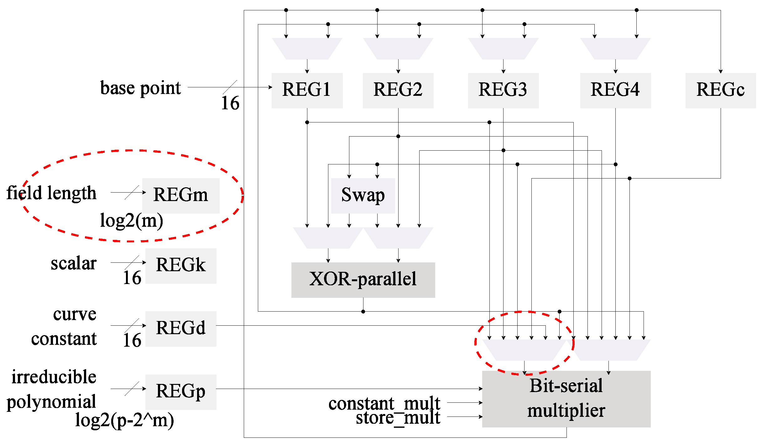
Figure 2 reflects the changes in the architectural design compared to the base architecture in Figure 1. For this second architecture it was necessary to include the field length as an additional input. This value is used to control the iterations in the Itoh-Tsujii inversion algorithm. One of the MUX that feeds the field multiplier input was required to be re-wired as well.
The implementation results for the kP architectures (comparing C0 and C1) can be found in Table 3.
From these results it can be noted how the modification of the inversion algorithm offers an average reduction of 7% in the energy consumption for different versions of the kP architecture. On the other hand, the hardware usage shows an average increment of 7%. This is consistent with the data in Table 2.
4.3. Modification 2: Field Multiplier
In the outlined second strategy, replacing the bit-serial multiplier with a digit multiplier is suggested. The new multiplier should be created with the same ports as the previous one to ease the interconnection; it ought to provide support for fast operations (which can be used to store data in the registers); and constant multiplications (with reduced length) should also be preserved. The new multiplier also needs to be parameterized in order to function for any digit size and any field length, preserving the generality of the design.
4.3.1. Digit-Based Multiplier
A digit-based multiplier, as presented in Algorithm 5, allows to explore area/latency tradeoffs for different applications. Implementing a digit-based multiplier makes it possible to explore how much hardware can be compromised in order to reduce the cycle count of the architecture. If the design is parameterized then a single architecture can be used for a wide range of applications.
| Algorithm 5 Digit Multiplication in Where d is the Digit Size [55]. |
| Input:, the irreducible polynomial of Output: for to 0 do end for return |
The digit multiplier from Algorithm 5 uses an underlying combinatorial multiplier:
The size of this combinatorial multiplier is what determines the hardware cost of the digit multiplier. A combinatorial multiplier can be seen as a matrix of hardware cells where its width is the digit size and its depth is the operand size.
4.3.2. Implementation of the Digit Multiplier
We designed a digit multiplier based on two combinatorial multipliers. The design was synthesized for the xc6slx16 FPGA. At this point, the number of IO ports in the digit multiplier makes the place-and-route process infeasible; some post-synthesis results are provided in Table 4.
The digit multiplier was integrated in the architecture C0 which uses the Wang inversion algorithm to generate a new architecture denominated C2. This aims to determine if the use of Itoh-Tsujii inversion is cost-effective when a dedicated squaring module is not implemented. In this case, as can be seen in Figure 3, the bit-serial multiplier is replaced with the digit multiplier. Only small changes in the input MUX are required.
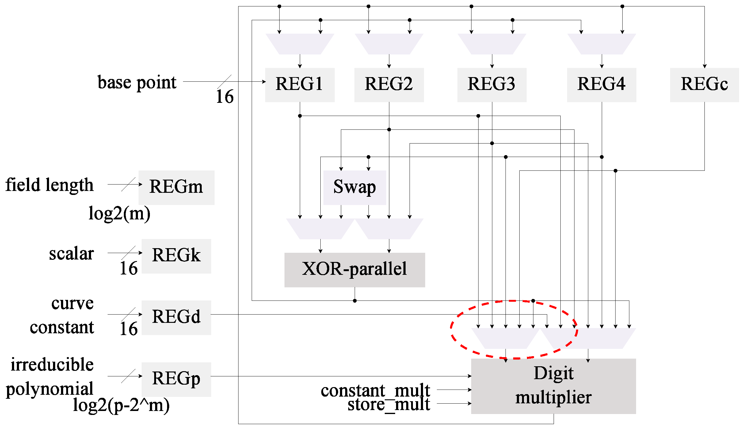
The multiplier was also merged into architecture C1 to generate the design shown in Figure 4. This architecture now has been modified with the first two proposed optimizations.
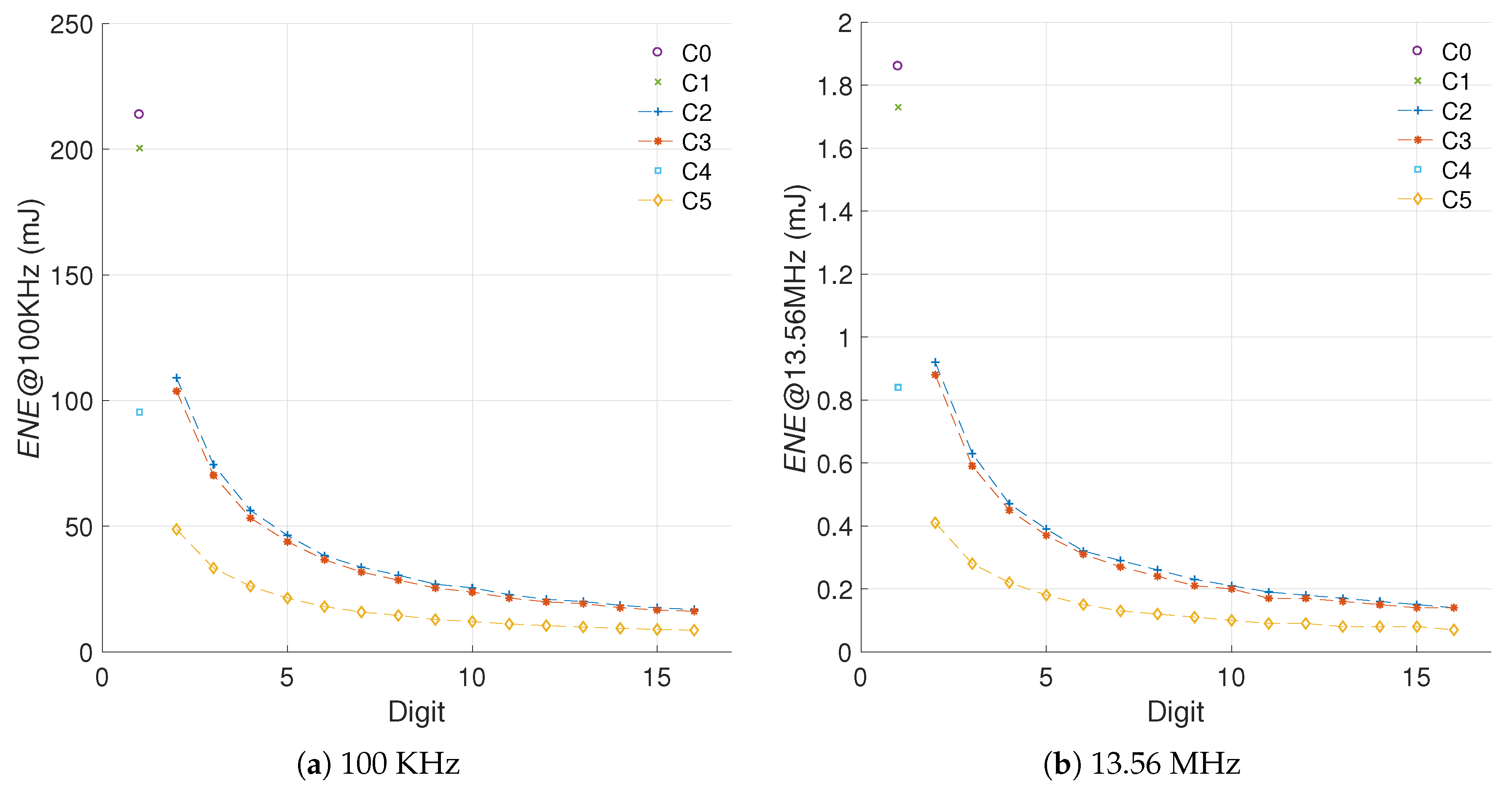
The implementation results for C2 and C3, which now use a digit multiplier, can be found in Table 5. Both designs were synthesized for the xc6slx16 FPGA using operational frequencies of 100 KHz and 13.56 MHz. These results are compared against the implementation results for C0 and C1 from Table 3. In this instance we are evaluating the efficiency of the digit multiplier (used in C2 and C3) compared with the bit-serial multiplier (used in C0 and C1).
The use of a digit multiplier enables achievement of a reduction in the energy ranging from 51% to 92% with hardware increments ranging from 6% to 54%. This trend seems to be consistent for both C2 and C3. The main difference between these architectures is that C3 has greater energy reduction for small digit sizes, which implies smaller hardware increments. In the long run (), however, both architectures tend to reach similar energy consumption levels.
4.4. Modification 3: Squaring Module
In the base architecture from Figure 1 the squaring operations are realized as multiplications. The selected kP algorithm performs four squarings per ladder step (). By including a dedicated squaring module the latency can be reduced since squarings are more efficient than multiplications in hardware. The C1 and C3 architectures (Figure 2 and Figure 4, respectively) can also benefit from this modification since the inversion method used (Algorithm 4) relies heavily on squarings. Although the advantages of a dedicated squaring component are evident, the hardware costs must be evaluated in order to assess its efficiency.
A combinatorial design for squarings was selected in order to maximize the latency reduction. Note that using a squaring module can reduce the latency independently of the field multiplier used. For this reason, we study both the alternative where the field multiplication uses a bit-serial approach but that also features dedicated squarings, and the option where the system uses a digit multiplier together with a squaring module.
4.4.1. Field Squarings
A squaring module is a special kind of field multiplier which exploits the fact that both input operands are the same word. The squaring procedure is presented in the following. Following this method, the squaring operation is reduced to a field multiplication of an bits word by a d bits word.
Let the input element A be represented as a polynomial :
Thus, the squaring of in polynomial form is obtained by shifting the polynomial’s coefficients to the left, generating a terms polynomial :
The coefficients in can be divided in two polynomials and , considering that the elements in are shifted positions to the left:
The coefficients in each of the new polynomials are:
Shifting the elements in can be solved as a multiplication by the element , which can be obtained from the finite field’s irreducible polynomial :
The final multiplication can be performed either using a bit-serial multiplier or a combinatorial multiplier. The latter was used for this work.
4.4.2. Implementation of the Squaring Module
The squaring module was included to the architectures that use the Itoh-Tsujii inversion algorithm (C1 and C3) to generate the versions C4 and C5 of the architecture, respectively. The architectural designs of C4 and C5 are illustrated in Figure 5.
In both modules the main difference is the addition of the squaring module, which has an effect on the MUXs at the input of the field multiplier. The MUXs at the input of the data registers were also updated to store the results of the squaring module.
The designs were implemented for the xc6slx16 FPGA using operational frequencies of 100 KHz and 13.56 MHz. Table 6 provides implementation results for the kP architectures which include a dedicated squaring module.
In the case where a bit-serial multiplier is used, the energy consumption is halved—compare C4 in Table 6 to C1 in Table 3. The addition of the squaring module enables achieving energy reductions ranging from 77% to 96% if a digit multiplier is used (C5). Comparing C5 to C3—where the reduction ranges from 51% to 92%, see Table 5—the improvement is noticeable. The hardware increment of implementing the squaring module is 20%.
4.5. Other Strategies
In a design which contains combinatorial logic and data registers, if these registers are not disconnected from the combinatorial logic spurious calculations will be performed. The switching activity on the combinatorial modules translates into power dissipation, and if the data being processed is not useful then it represents energy being wasted. In order to mitigate the spurious calculations, it is a good design practice to insulate the data registers. This applies both for inputs and outputs. If storing the data is not required, then the register writing must be disabled; if the data in the register is not needed, then it should be masked with zeros.
Register insulation is built-in in the proposed designs. As can be noted from Figure 1, Figure 2, Figure 3, Figure 4 and Figure 5 the data registers outputs are always connected to a MUX element. These modules, under all cases default to GND when the output is not required, effectively insulating the data in the registers from reaching any combinatorial module.
We evaluated the impact of removing the register insulation from our designs. Although this strategy has a hardware cost and contributes to reducing the power dissipation, the variation is not significant—13% less energy in the best case and 10% more hardware in the worst case.
4.6. Summary
Table 7 provides a summary of all the designs studied in this section.
5. Energy Savings in Relation to Area Costs
In this section we describe the design and application of a method to evaluate the efficiency of the optimization techniques that were used to create the kP architectures C1–C5. This section is conformed of two parts: first we describe a novel method for quantifying the efficiency of energy optimizations in regards to area cost, then we use this method for comparing our work with other state of the art solutions.
For the analysis provided in this section we consider that the configurations C0, C1, and C4 are equivalent to the configurations C2, C3, and C5 when , respectively.
5.1. Novel Metric for Efficiency of Energy Oriented Optimizations in Regards to Area Costs
Since it is complicated to characterize the efficiency of an optimization technique in terms of area or energy, we have developed an evaluation metric which can account for both magnitudes.
We start from the energy evaluation and area cost of all the hardware implementations. Figure 6 shows the area (FF, LUT, SLC), power (POW), and energy (ENE) results for the different kP architectures under study.
In this work we describe four challenges which should be surpassed for an evaluation metric aimed at comparing hardware realizations; these challenges are described in the following.
5.1.1. Selecting the Data
In FPGA implementations it is customary to use SLCs as area unit. However, as it can be seen from Figure 6, the SLC measurements are prone to outliers. This occurs due to the nature of the PAR process which follows heuristic approaches. In the ideal case the number of SLC should be correlated with the number of FFs and LUTs placed in the design. For example, for the FPGA used in our experiments, each SLC contains four FFs, four LUTS, and some connection logic.
The number of FFs required by the kP architectures is given by the number of registers allocated. The modifications applied do not modify the number of registers substantially, which is why this value remains almost constant. In contrast, since most of the changes made require combinatorial logic, we can observe that the amount of LUTs varies steadily. With this reasoning, we propose to use LUTs as area indicator for the configurations evaluated. The first challenge for the proposed metric is to define whether the LUT results can be used to represent the hardware increment in the design accurately.
In regards to power dissipation and energy consumption, the quiescent component in FPGAs is almost constant and more significant than its dynamic counterpart; this makes it easier to study the energy profile of an architecture.
To measure the area and energy increments we use percentile differences (%). The variation, difference, or increment in the measurement of a particular metric () for the architecture , with regards to a previous observation () for the architecture can be computed as in (8).
Figure 7 shows the area and energy s for the different architectures created. It is important to recall that in the proposed scheme a positive difference implies an increment, like in the case of area, and a negative difference implies a decrement, like in the case of energy consumption.
From the results in Figure 7 we can note that in fact, the LUT usage is a close match to the SLC in regards to perceived hardware cost, with less impact from outliers. The R-square yields a closeness of 74.54%, 98.21% and 16.45% for C2, C3, and C5, respectively. Even though the R-square in the case of C5 is not great, the goodness-of-fit achieved for C2 and C3 hints that the LUT measurements can substitute the SLC as area units when the number of FFs remains constant. This solves the first challenge proposed.
5.1.2. Efficiency Metric
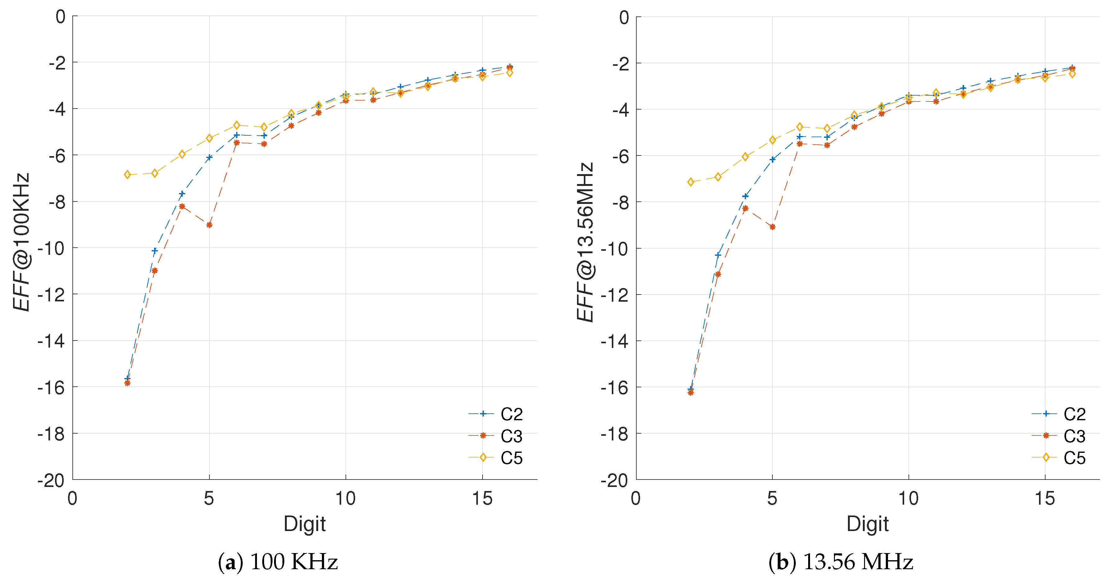
Using the LUT and ENE results we propose the efficiency (EFF) metric in (24). What this value conveys is the energy decrement weighted by the area increments associated with the improvement. If the energy savings are high (negative percentages), and the area costs for said improvements are low (in relation to a reference model) then the efficiency metric will yield a high negative result. Results that are less negative imply that the area cost outweighs the energy savings achieved.
Figure 8 presents the evaluation of the efficiency metric for the different architectures created.
5.1.3. Sensitivity to Frequency Variations
For the results in Figure 8 we used an operational frequency of 100 KHz. However, how does the operational frequency affect the proposed evaluation metric? This is the second challenge for our metric. This question is important for comparing our results with proposals from the literature. It is evident that not all the works would use the same operational frequency. Furthermore, given the relevance of this magnitude in the energy consumption of a design, it is clear that any evaluation metric should account for frequency variations.
Figure 9 illustrates the differences in the energy consumption for the kP architectures under evaluation as a result of changing the operational frequency.
As it can be noted, even though the measured values vary by two orders of magnitude, the consumption models are similar. In fact, both energy measurements can be used for computing the energy increment of each architecture, and later the efficiency evaluation using both operational frequencies.
The evaluation of the efficiency metric for two operational frequencies is provided in Figure 10. The results demonstrate that the proposed metric can account for variations in the operational frequency of the implementation. In these results, the R-square for the configurations C2, C3, and C5 indicates goodness values of 99.87%, 99.91%, and 99.62%, respectively. This answers the second challenge proposed, since the metric proposed appears to be able to isolate the strong influence that the frequency has on the static power consumption, while highlighting the improvements achieved by the architecture modifications on the dynamic power consumption.
5.1.4. Sensitivity to Different Curve Sizes
How does the curve length influence the results? This is considered the third challenge proposed. In this work we use the elliptic curve BE251 as case study. However, when comparing our work with the literature, it is noteworthy that most existing lightweight proposals of elliptic curve systems target security levels of at most 80 bits. Since our work targets security levels close to 128 bits, the necessity of accounting for the difference in field length is clear.
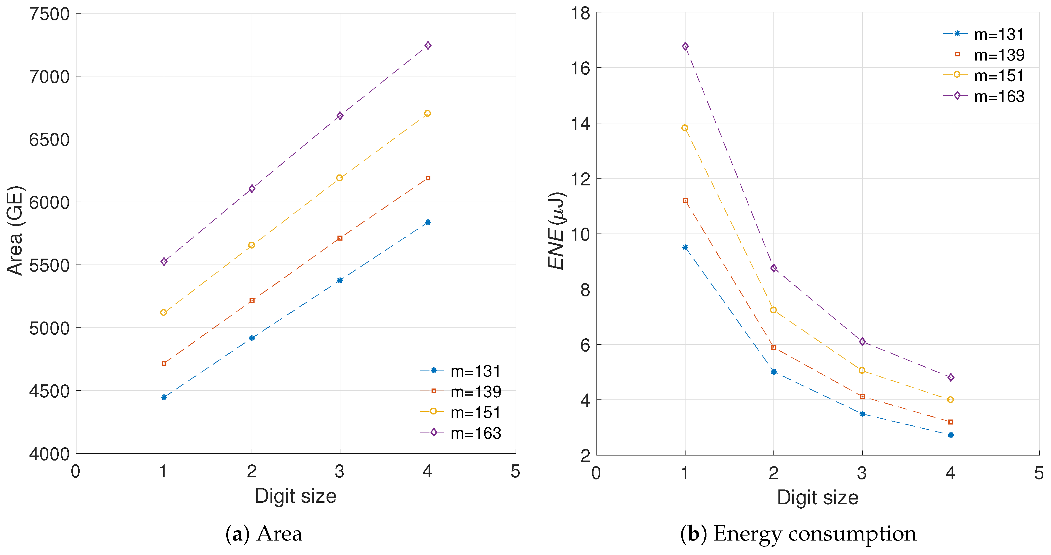
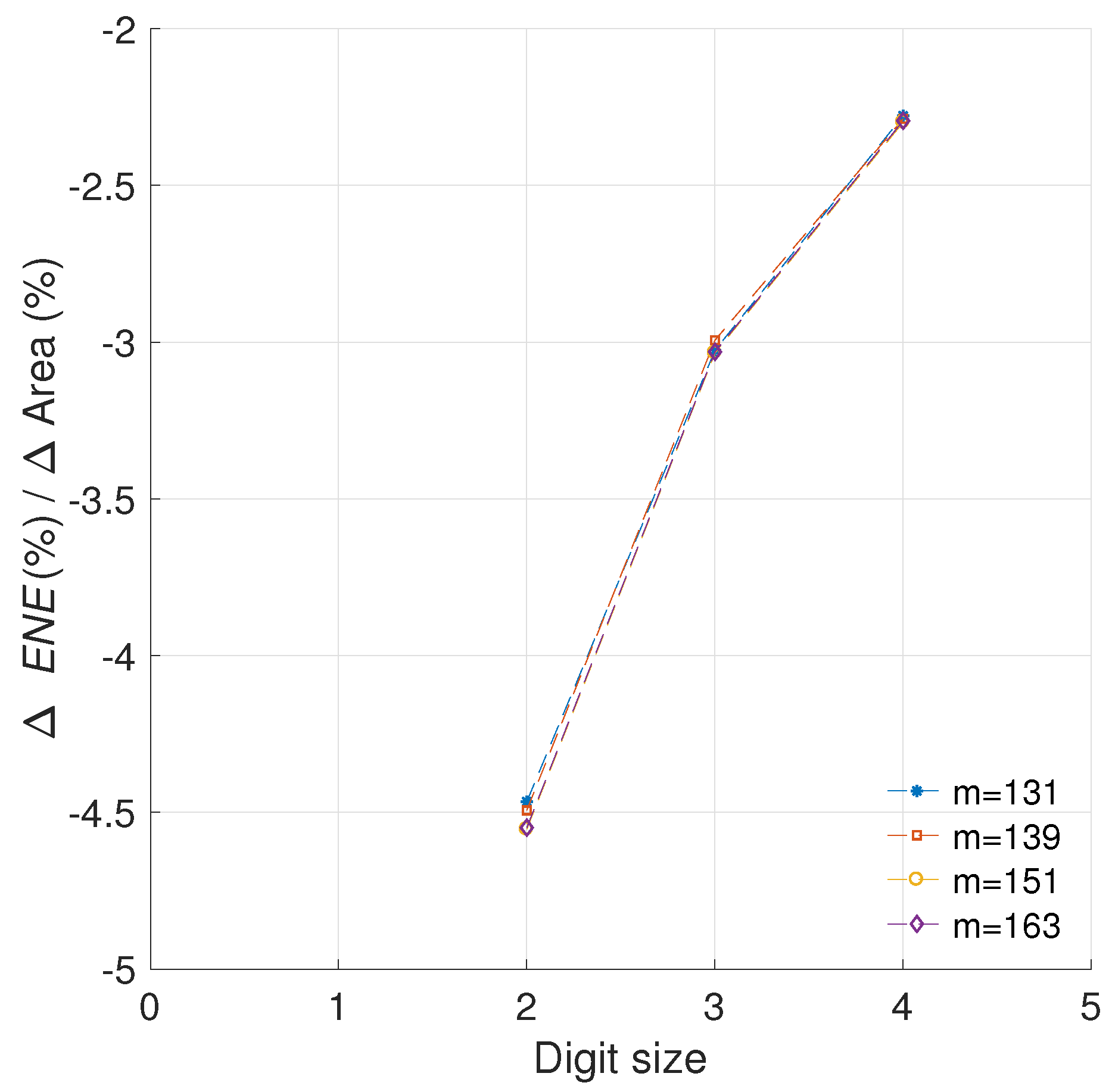
We have used the results provided in [22] to evaluate the sensitivity of the proposed metric to differences in the curve length. The relevance of that work is that the authors present implementation results for a scalar multiplication architecture using generic elliptic curves of varying length. We took their area and energy results and utilized them to evaluate our metric. Figure 11 illustrates the area and energy results from [22] for various curve lengths. Figure 12 presents the evaluation of the proposed metric using the results from [22]. In this case the area increments are measured in GEs and the energy increments in J.
As it can be noted from Figure 12, our metric yields similar calculations for the different experiments which use varying curve lengths. These figures generate R-square evaluations of 99.99%, 99.99%, and 99.99%, which implies a close match in the values. Based on this experiment, we can conclude that the proposed metric is not sensitive to variations in the curve length, which solves the third challenge presented. This is a significant result as it implies that in comparing our results with the state of the art it is not necessary to account for variations in the curve length.
5.1.5. Sensitivity to the Implementation Technology
As evidenced in the previous point, not all works in the literature target FPGA technology. Some of them, as in the case of [22], have been developed for ASIC. Even though our metric can be applied to both scenarios without problems, it is necessary to determine if changing the implementation technology can impact the results of the proposed metric for the same architecture. However, our work focuses on FPGA technology and in the literature we have not identified any work which allows carrying out this experiment. As of now, we consider this fourth question as an open challenge.
5.2. Applying the Proposed Metric for Comparing Our Work with the State of the Art
All of the reviewed works which propose low-power or low-energy kP architectures use digit multipliers. This is understandable, given how a digit multiplier allows for significant improvements in the reduction of the energy consumption with relative low hardware costs.
The metric proposed is particularly useful for comparing such works. For starters, the ability of synthesizing a design for varying digit sizes allows flexibility of the application. Some scopes might be able to accommodate greater hardware strains in order to achieve improved performance, whereas others can have stricter area bounds. Therefore, an architecture of this type cannot be evaluated solely on the efficiency for a particular digit size. The curves derived from the evaluation of the efficiency metric proposed, as a function of the digit size in architectures with digit multipliers, make it possible to use the area under the curve as an objective quantifier of efficiency. To this end different problems need to be addressed.
First, since in this case of comparison we refer to the efficiency of a particular architecture which uses a digit multiplier, each series shall use as reference the instance of the implementation where . In this scenario we aim at quantifying the efficiency of an individual architecture. The relative percentile increments can be computed as in (25).
Second, to use the area under the curve as quantifier it is necessary that the evaluation bounds are coincident for each configuration. That is, that all the designs evaluated provide implementation results for the same digit interval. The case where is mandatory since it is used as reference, but as upper bound we can define any .
Once the evaluation boundaries have been defined, we note that the majority of works in the literature do not provide results for continuous intervals of the digit space. For instance, the works in [17] and [25] only provide implementation results for the cases where and , respectively. A solution for this problem is to use interpolation models in order to obtain the missing data.
5.2.1. Modeling the Data
The area and energy increments are the source for computing the efficiency of a design. These increments are calculated from the raw data of hardware resources and energy consumption. The former can be modeled using a polynomial fit of first degree of the form while the latter can be adjusted to an exponential model of the form where are constants for the model of each configuration and is the digit size. The model proposed for the efficiency metric is presented in (26).
The use of a mathematical model over the raw data has the additional advantage that the effects of outliers are mitigated. This is practical since some works from the literature that target FPGAs do not provide LUT results [25] or do provide them but the variance in the flip flop count is significant [17].
In Figure 13 we show the models obtained for the area and energy results from our C2, C3, and C5 architectures. Consequently, Figure 14 presents the evaluation of the efficiency metric applied over these data. It is possible to observe the precision obtained in the final model, which produces R-square evaluations of 93.12%, 93.66% for C2 and C3, respectively.
As can be observed in Figure 13, the area in LUTs recorded for the configuration C5 where is an outlier. When this anomalous reference point is used for evaluating (24), the results are skewed. Modeling the data prevents obtaining erroneous results by removing the outliers. This is the reason for the significant variation exhibited between C5 and .
With the updated analysis we can note that the most cost effective solution provided in this work, in regards to preserving the implementation area while reducing the energy profile, is the architecture C5. This design consistently outperforms the other configurations for any digit size.
5.2.2. Quantifying the Efficiency
The data in Figure 14 can be used to obtain the area under the curve for each configuration using a trapezoidal rule as shown in Equation (27).
For this evaluation we shall define and since . From this, the configurations C2, C3, and C5 obtain efficiency scores of −77.59, −80.16, and −97.5, respectively. In this evaluation, the configuration C5 is the one that achieves the greater energy reduction per area cost overall.
5.2.3. Comparison with the Literature
Table 8 provides implementation results from works in the literature that are defined as “low power” or “low energy” by their authors. Using these data we have adjusted coefficients for the model of the area and energy measurements from each work. These models are used for evaluating the efficiency metric and to obtain the respective efficiency score for each design. In 77% of the non-trivial models we achieved R-square evaluations above 99%, which implies that the provided results are accurate. Table 9 provides the coefficients obtained for the model of each configuration, according to the formula in Equation (26).
Figure 15 illustrates the evaluation of the efficiency metric for the different works in the state of the art.
Finally, the efficiency scores for each configuration evaluated are reported in Figure 16.
5.3. Limitations of the Proposed Method
The proposed method is sensitive to data outliers. Since the results are provided as percentages, when the measurements are small, area or energy variations can skew the results. This is solved by using models to adjust the data.
Conditions that do not adjust to the models proposed also lead to unexpected results. If the energy consumption is not reduced or the hardware requirements are not increased, the sign of the results will flop and produce spurious evaluations of (27). While that might have some use, for the purposes intended in this article such results are undesired.
6. Conclusions
In this paper we have studied the reduction of energy consumption in six different scalar multiplication architectures. Starting from a base low-area design, we have improved it following energy and power reducing strategies. The result of this process is a comprehensive set of designs that have gradual optimization levels, and thus exhibit from moderate to increased area/energy tradeoffs. These scalar multiplication modules can be used in key establishment systems with low-area requirements and low-energy consumption.
The novel metric proposed can be applied in studying the impact of any modification to a reference architecture, implemented in hardware. In a sense, it represents the energy costs, weighted by the associated hardware costs. The main goal for using this indicator is to demonstrate the effectiveness of any energy-related improvement in a platform with hardware constraints. We have shown that this metric is capable of accounting for differences in the area units, the operational frequency, and the field size; we also provided a way to reduce its sensitivity to unavailable data and outliers. For these reasons we believe that it is adequate for comparing works implemented under heterogeneous conditions.
From the proposed architectures, the configuration C5 exhibits the greatest efficiency. This design employs a digit-multiplier, the Itoh-Tsujii inversion algorithm, and a dedicated squaring module; and also implements datapath insulation. Compared against the state of the art, this configuration turned out to be 13.33% more efficient than the closest work. In terms of efficiency, our proposal represents a good candidate for implementation in environments with area and energy constraints such as IoT devices.
Author Contributions
Conceptualization, C.A.L.-N., A.D.-P. and M.M.-S.; Data curation, C.A.L.-N.; Formal analysis, C.A.L.-N.; Funding acquisition, A.D.-P. and M.M.-S.; Investigation, C.A.L.-N.; Methodology, C.A.L.-N., A.D.-P. and M.M.-S.; Project administration, A.D.-P. and M.M.-S.; Resources, A.D.-P. and M.M.-S.; Software, C.A.L.-N.; Supervision, A.D.-P. and M.M.-S.; Validation, C.A.L.-N.; Visualization, C.A.L.-N.; Writing—original draft, C.A.L.-N.; Writing—review & editing, C.A.L.-N., A.D.-P. and M.M.-S.
Funding
This research was funded by CONACyT Mexico, grant number 336750. The research was also funded by “Fondo Sectorial de Investigación para la Educación”, CONACyT Mexico, through the project number 281565.
Acknowledgments
The authors would like to thank CINVESTAV for the support received. The authors would like to express their gratitude with the reviewers, in particular reviewer 2, for their remarkable contributions which helped to improve the quality of this manuscript.
Conflicts of Interest
The authors declare no conflict of interest. The funders had no role in the design of the study; in the collection, analyses, or interpretation of data; in the writing of the manuscript, or in the decision to publish the results.
References
- Mangia, M.; Pareschi, F.; Rovatti, R.; Setti, G. Low-Cost Security of IoT Sensor Nodes With Rakeness-Based Compressed Sensing: Statistical and Known-Plaintext Attacks. IEEE Trans. Inf. Forensics Secur. 2018, 13, 327–340. [Google Scholar] [CrossRef]
- Kumar, P.; Lee, H.J. Security Issues in Healthcare Applications Using Wireless Medical Sensor Networks: A Survey. Sensors 2012, 12, 55–91. [Google Scholar] [CrossRef] [PubMed]
- Perez-Torres, R.; Torres-Huitzil, C.; Galeana-Zapien, H. An On-Device Cognitive Dynamic Systems Inspired Sensing Framework for the IoT. IEEE Commun. Mag. 2018, 56, 154–161. [Google Scholar] [CrossRef]
- Khan, M.K.; Alghathbar, K. Cryptanalysis and Security Improvements of ‘Two-Factor User Authentication in Wireless Sensor Networks’. Sensors 2010, 10, 2450–2459. [Google Scholar] [CrossRef] [PubMed]
- Buratti, C.; Conti, A.; Dardari, D.; Verdone, R. An Overview on Wireless Sensor Networks Technology and Evolution. Sensors 2009, 9, 6869–6896. [Google Scholar] [CrossRef] [PubMed]
- Ghiasi, S.; Srivastava, A.; Yang, X.; Sarrafzadeh, M. Optimal Energy Aware Clustering in Sensor Networks. Sensors 2002, 2, 258–269. [Google Scholar] [CrossRef]
- Liu, M.; Cao, J.; Chen, G.; Wang, X. An Energy-Aware Routing Protocol in Wireless Sensor Networks. Sensors 2009, 9, 445–462. [Google Scholar] [CrossRef]
- Liu, Z.; Seo, H. IoT-NUMS: Evaluating NUMS Elliptic Curve Cryptography for IoT Platforms. IEEE Trans. Inf. Forensics Secur. 2019, 14, 720–729. [Google Scholar] [CrossRef]
- Yeh, H.L.; Chen, T.H.; Liu, P.C.; Kim, T.H.; Wei, H.W. A Secured Authentication Protocol for Wireless Sensor Networks Using Elliptic Curves Cryptography. Sensors 2011, 11, 4767–4779. [Google Scholar] [CrossRef]
- Piedra, A.d.l.; Braeken, A.; Touhafi, A. Extending the IEEE 802.15.4 Security Suite with a Compact Implementation of the NIST P-192/B-163 Elliptic Curves. Sensors 2013, 13, 9704–9728. [Google Scholar] [CrossRef]
- Liu, Z.; Liu, D.; Zou, X.; Lin, H.; Cheng, J. Design of an Elliptic Curve Cryptography Processor for RFID Tag Chips. Sensors 2014, 14, 17883–17904. [Google Scholar] [CrossRef] [PubMed]
- Choi, Y.; Lee, D.; Kim, J.; Jung, J.; Nam, J.; Won, D. Security Enhanced User Authentication Protocol for Wireless Sensor Networks Using Elliptic Curves Cryptography. Sensors 2014, 14, 10081–10106. [Google Scholar] [CrossRef] [PubMed]
- Liu, Z.; Seo, H.; Großschädl, J.; Kim, H. Efficient Implementation of NIST-Compliant Elliptic Curve Cryptography for 8-bit AVR-Based Sensor Nodes. IEEE Trans. Inf. Forensics Secur. 2016, 11, 1385–1397. [Google Scholar] [CrossRef]
- Barker, E. NIST Special Publication 800-57. Part 1. Revision 4. Recommendation for Key Management. 2016. Available online: http://nvlpubs.nist.gov/nistpubs/SpecialPublications/NIST.SP.800-57pt1r4.pdf (accessed on 15 October 2018).
- Lara-Nino, C.A.; Diaz-Perez, A.; Morales-Sandoval, M. Elliptic Curve Lightweight Cryptography: A Survey. IEEE Access 2018, 6, 72514–72550. [Google Scholar] [CrossRef]
- Schroeppel, R.; Beaver, C.; Gonzales, R.; Miller, R.; Draelos, T. A Low-Power Design for an Elliptic Curve Digital Signature Chip. In Cryptographic Hardware and Embedded Systems, Proceedings of the CHES 2002, 4th International Workshop, Redwood Shores, CA, USA, 13–15 August 2002; Revised Papers; Kaliski, B.S., Koç, ç.K., Paar, C., Eds.; Springer: Berlin/Heidelberg, Germany, 2003; pp. 366–380. [Google Scholar]
- Keller, M.; Byrne, A.; Marnane, W.P. Elliptic Curve Cryptography on FPGA for Low-Power Applications. ACM Trans. Reconfigurable Technol. Syst. 2009, 2, 2. [Google Scholar] [CrossRef]
- Keller, M.; Marnane, W. Energy Efficient Elliptic Curve Processor. In Integrated Circuit and System Design. Power and Timing Modeling, Optimization and Simulation, Proceedings of the 18th International Workshop, PATMOS 2008, Lisbon, Portugal, 10–12 September; Revised Selected Papers; Svensson, L., Monteiro, J., Eds.; Springer: Berlin/Heidelberg, Germany, 2009; pp. 287–296. [Google Scholar]
- Tamura, M.; Ikeda, M. 1.68uJ/signature-generation 256-bit ECDSA over GF(p) signature generator for IoT devices. In Proceedings of the 2016 IEEE Asian Solid-State Circuits Conference (A-SSCC), Toyama, Japan, 7–9 November 2016; pp. 341–344. [Google Scholar]
- Asif, S.; Andersson, O.; Rodrigues, J.; Kong, Y. 65-nm CMOS low-energy RNS modular multiplier for elliptic-curve cryptography. IET Comput. Digit. Tech. 2018, 12, 62–67. [Google Scholar] [CrossRef]
- Öztürk, E.; Sunar, B.; Savaş, E. Low-Power Elliptic Curve Cryptography Using Scaled Modular Arithmetic. In Cryptographic Hardware and Embedded Systems, Proceedings of the CHES 2004, 6th International Workshop, Cambridge, MA, USA, 11–13 August 2004; Joye, M., Quisquater, J.J., Eds.; Springer: Berlin/Heidelberg, Germany, 2004; pp. 92–106. [Google Scholar]
- Batina, L.; Mentens, N.; Sakiyama, K.; Preneel, B.; Verbauwhede, I. Low-Cost Elliptic Curve Cryptography for Wireless Sensor Networks. In Security and Privacy in Ad-Hoc and Sensor Networks, Proceedings of the Third European Workshop, ESAS 2006, Hamburg, Germany, 20–21 September 2006; Revised Selected Papers; Buttyán, L., Gligor, V.D., Westhoff, D., Eds.; Springer: Berlin/Heidelberg, Germany, 2006; pp. 6–17. [Google Scholar]
- Bernstein, D.J.; Lange, T.; Rezaeian Farashahi, R. Binary Edwards Curves. In Cryptographic Hardware and Embedded Systems, Proceedings of the CHES 2008, 10th International Workshop, Washington, DC, USA, 10–13 August 2008; Springer: Berlin/Heidelberg, Germany, 2008; pp. 244–265. [Google Scholar]
- Koziel, B.; Azarderakhsh, R.; Mozaffari-Kermani, M. Low-Resource and Fast Binary Edwards Curves Cryptography. In Progress in Cryptology, Proceedings of the INDOCRYPT 2015: 16th International Conference on Cryptology in India, Bangalore, India, 6–9 December 2015; Springer International Publishing: Cham, Switzerland, 2015; pp. 347–369. [Google Scholar]
- Keller, M.; Marnane, W. Low Power Elliptic Curve Cryptography. In Integrated Circuit and System Design. Power and Timing Modeling, Optimization and Simulation, Proceedings of the 17th International Workshop, PATMOS 2007, Gothenburg, Sweden, 3–5 September 2007; Azémard, N., Svensson, L., Eds.; Springer: Berlin/Heidelberg, Germany, 2007; pp. 310–319. [Google Scholar]
- Kocabas, U.; Fan, J.; Verbauwhede, I. Implementation of Binary Edwards Curves for very-constrained devices. In Proceedings of the ASAP 2010, Rennes, France, 7–9 July 2010; pp. 185–191. [Google Scholar]
- Dan, Y.P.; He, H.L. Tradeoff Design of Low-Cost and Low-Energy Elliptic Curve Crypto-Processor for Wireless Sensor Networks. In Proceedings of the 2012 8th International Conference on Wireless Communications, Networking and Mobile Computing, Shanghai, China, 21–23 September 2012; pp. 1–5. [Google Scholar]
- Knežević, M.; Nikov, V.; Rombouts, P. Low-Latency Encryption—Is “Lightweight = Light + Wait”? In Proceedings of the Cryptographic Hardware and Embedded Systems, CHES 2012, Leuven, Belgium, 9–12 September 2012; Prouff, E., Schaumont, P., Eds.; Springer: Berlin/Heidelberg, Germany, 2012; pp. 426–446. [Google Scholar]
- Purnaprajna, M.; Puttmann, C.; Porrmann, M. Power Aware Reconfigurable Multiprocessor for Elliptic Curve Cryptography. In Proceedings of the 2008 Design, Automation and Test in Europe, Munich, Germany, 10–14 March 2008; pp. 1462–1467. [Google Scholar]
- Ahmadi, H.R.; Afzali-Kusha, A. A low-power and low-energy flexible GF(p) elliptic-curve cryptography processor. J. Zhejiang Univ. Sci. C 2010, 11, 724–736. [Google Scholar] [CrossRef]
- Iwasaki, A.; Shibata, Y.; Oguri, K.; Harasawa, R. An energy-efficient FPGA-based soft-core processor with a configurable word size ECC arithmetic accelerator. In Proceedings of the 2015 IEEE Symposium in Low-Power and High-Speed Chips (COOL CHIPS XVIII), Yokohama, Japan, 13–15 April 2015; pp. 1–3. [Google Scholar]
- Rožić, V.; Reparaz, O.; Verbauwhede, I. A 5.1 uJ per point-multiplication elliptic curve cryptographic processor. Int. J. Circuit Theory Appl. 2017, 45, 170–187. [Google Scholar] [CrossRef]
- Liu, Z.; Weng, J.; Hu, Z.; Seo, H. Efficient Elliptic Curve Cryptography for Embedded Devices. ACM Trans. Embed. Comput. Syst. 2016, 16, 53. [Google Scholar] [CrossRef]
- Liu, Z.; Huang, X.; Hu, Z.; Khan, M.K.; Seo, H.; Zhou, L. On Emerging Family of Elliptic Curves to Secure Internet of Things: ECC Comes of Age. IEEE Trans. Dependable Secur. Comput. 2016, 14, 237–248. [Google Scholar]
- Chandrakasan, A.P.; Potkonjak, M.; Mehra, R.; Rabaey, J.; Brodersen, R.W. Optimizing Power Using Transformations. Trans. Comp.-Aided Des. Integr. Cir. Syst. 2006, 14, 12–31. [Google Scholar] [CrossRef]
- Kim, H.; Kim, Y.; Yoo, H.J. A 6.3nJ/op low energy 160-bit modulo-multiplier for elliptic curve cryptography processor. In Proceedings of the 2008 IEEE International Symposium on Circuits and Systems, Seattle, WA, USA, 18–21 May 2008; pp. 3310–3313. [Google Scholar]
- Gaubatz, G.; Kaps, J.P.; Ozturk, E.; Sunar, B. State of the art in ultra-low power public key cryptography for wireless sensor networks. In Proceedings of the Third IEEE International Conference on Pervasive Computing and Communications Workshops, Kauai Island, HI, USA, 8–12 March 2005; pp. 146–150. [Google Scholar]
- Fan, J.; Reparaz, O.; Rožić, V.; Verbauwhede, I. Low-energy encryption for medical devices: Security adds an extra design dimension. In Proceedings of the 2013 50th ACM/EDAC/IEEE Design Automation Conference (DAC), Austin, TX, USA, 29 May–7 June 2013; pp. 1–6. [Google Scholar]
- Maidhili, R.; Karthik, G. Energy Efficient and Secure Multi-User Broadcast Authentication Scheme in Wireless Sensor Networks. In Proceedings of the 2018 International Conference on Computer Communication and Informatics (ICCCI), Coimbatore, India, 4–6 January 2018; pp. 1–6. [Google Scholar]
- Kreiser, D.; Dyka, Z.; Kabin, I.; Langendoerfer, P. Low-energy key exchange for automation systems. In Proceedings of the 2018 13th International Conference on Design Technology of Integrated Systems In Nanoscale Era (DTIS), Taormina, Italy, 9–12 April 2018; pp. 1–5. [Google Scholar]
- Hein, D.; Wolkerstorfer, J.; Felber, N. ECC Is Ready for RFID—A Proof in Silicon. In Selected Areas in Cryptography, Proceedings of the 15th International Workshop, SAC 2008, Sackville, NB, Canada, 14–15 August 2009; Revised Selected Papers; Avanzi, R.M., Keliher, L., Sica, F., Eds.; Springer: Berlin/Heidelberg, Germany, 2009; pp. 401–413. [Google Scholar]
- Kodali, R.K.; Patel, K.H.; Sarma, N. Energy efficient elliptic curve point multiplication for WSN applications. In Proceedings of the 2013 National Conference on Communications (NCC), New Delhi, India, 15–17 February 2013; pp. 1–5. [Google Scholar]
- Ting, P.; Tsai, J.; Wu, T. Signcryption Method Suitable for Low-Power IoT Devices in a Wireless Sensor Network. IEEE Syst. J. 2018, 12, 2385–2394. [Google Scholar] [CrossRef]
- De Clercq, R.; Uhsadel, L.; Van Herrewege, A.; Verbauwhede, I. Ultra Low-Power Implementation of ECC on the ARM Cortex-M0+. In Proceedings of the 51st Annual Design Automation Conference, DAC ’14, San Francisco, CA, USA, 1–5 June 2014; ACM: New York, NY, USA, 2014; pp. 112:1–112:6. [Google Scholar]
- Zeidler, S.; Goderbauer, M.; Krstić, M. Design of a low-power asynchronous elliptic curve cryptography coprocessor. In Proceedings of the 2013 IEEE 20th International Conference on Electronics, Circuits, and Systems (ICECS), Abu Dhabi, UAE, 8–11 December 2013; pp. 569–572. [Google Scholar]
- Targhetta, A.D.; Owen, D.E.; Israel, F.L.; Gratz, P.V. Energy-efficient Implementations of GF (P) and GF(2M) Elliptic Curve Cryptography. In Proceedings of the 2015 33rd IEEE International Conference on Computer Design (ICCD), ICCD ’15, New York, NY, USA, 18–21 October 2015; IEEE Computer Society: Washington, DC, USA, 2015; pp. 704–711. [Google Scholar]
- Tan, X.; Dong, M.; Wu, C.; Ota, K.; Wang, J.; Engels, D.W. An Energy-Efficient ECC Processor of UHF RFID Tag for Banknote Anti-Counterfeiting. IEEE Access 2017, 5, 3044–3054. [Google Scholar] [CrossRef]
- Dao, V.L.; Nguyen, V.T.; Hoang, V.P. Low Power ECC Implementation on ASIC. In Advances in Information and Communication Technology, Proceedings of the International Conference, ICTA 2016, Thai Nguyen, Vietnam, 12–12 December 2016; Akagi, M., Nguyen, T.T., Vu, D.T., Phung, T.N., Huynh, V.N., Eds.; Springer International Publishing: Cham, Switzerland, 2017; pp. 332–339. [Google Scholar]
- Rabaey, J. Low Power Design Essentials, 1st ed.; Springer Publishing Company: Berlin/Heidelberg, Germany, 2009; Incorporated. [Google Scholar]
- Liu, D.; Liu, Z.; Yong, Z.; Zou, X.; Cheng, J. Design and Implementation of an ECC-Based Digital Baseband Controller for RFID Tag Chip. IEEE Trans. Ind. Electron. 2015, 62, 4365–4373. [Google Scholar] [CrossRef]
- Itoh, T.; Tsujii, S. A Fast Algorithm for Computing Multiplicative Inverses in GF(2M) Using Normal Bases. Inf. Comput. 1988, 78, 171–177. [Google Scholar] [CrossRef]
- Daepp, U.; Gorkin, P. Fermat’s Little Theorem. In Reading, Writing, and Proving: A Closer Look at Mathematics; Springer: New York, NY, USA, 2011; pp. 315–323. [Google Scholar]
- Liskov, M. Fermat’s Little Theorem. In Encyclopedia of Cryptography and Security; van Tilborg, H.C.A., Jajodia, S., Eds.; Springer: Boston, MA, USA, 2011; p. 456. [Google Scholar]
- Guajardo, J. Itoh–Tsujii Inversion Algorithm. In Encyclopedia of Cryptography and Security; van Tilborg, H.C.A., Ed.; Springer: Boston, MA, USA, 2005; p. 313. [Google Scholar]
- Rodríguez-Henríquez, F.; Saqib, N.A.; Díaz-Pérez, A.; Koc, C.K. Cryptographic Algorithms on Reconfigurable Hardware (Signals and Communication Technology); Springer-Verlag New York, Inc.: Secaucus, NJ, USA, 2006. [Google Scholar]
Figure 1.
Low-area kP architecture, in the following referred to as C0.

Figure 2.
Architecture for kP featuring Itoh-Tsujii inversion (C1).

Figure 3.
Architecture C2 for kP, Wang inversion and a digit-multiplier are used.

Figure 4.
The Itoh-Tsujii inversion is paired with a digit-multiplier on this kP architecture (C3).

Figure 5.
Architectures for kP featuring dedicated squaring modules.

Figure 6.
FPGA area, power dissipation, and energy consumption for the different kP architectures.

Figure 7.
Percentile area and energy increments for architectures C2, C3, and C5 with reference to C0.
Figure 7.
Percentile area and energy increments for architectures C2, C3, and C5 with reference to C0.

Figure 8.
Evaluation of the efficiency metric for the different kP configurations.

Figure 9.
Energy consumption of the kP architectures at different operational frequencies.

Figure 10.
Evaluation of the efficiency metric for the different kP configurations using two operational frequencies.
Figure 10.
Evaluation of the efficiency metric for the different kP configurations using two operational frequencies.

Figure 11.
Implementation results for the architectures in [22].
Figure 11.
Implementation results for the architectures in [22].

Figure 12.
Evaluation of the efficiency metric for the results from [22].
Figure 12.
Evaluation of the efficiency metric for the results from [22].

Figure 13.
Curve fitting for the hardware usage and energy consumption of architectures C2, C3, and C5.
Figure 13.
Curve fitting for the hardware usage and energy consumption of architectures C2, C3, and C5.

Figure 14.
Evaluation of the efficiency metric for the C2, C3, and C5 configurations based on model data (), compared to the evaluation based on real data (EFF).
Figure 14.
Evaluation of the efficiency metric for the C2, C3, and C5 configurations based on model data (), compared to the evaluation based on real data (EFF).

Figure 15.
Evaluation of the efficiency metric for the different works in the literature, ours included.
Figure 15.
Evaluation of the efficiency metric for the different works in the literature, ours included.

Figure 16.
Efficiency scores for the different architectures in the literature. Values that are more negative represent greater energy savings overall.
Figure 16.
Efficiency scores for the different architectures in the literature. Values that are more negative represent greater energy savings overall.


Table 1.
Inversion algorithms cost over binary fields of variable length. Let and the binary representation of m, where represents the Hamming weight of w.
Table 1.
Inversion algorithms cost over binary fields of variable length. Let and the binary representation of m, where represents the Hamming weight of w.
| Inv. | Field | Multiplications | Squarings | Storage Bits |
|---|---|---|---|---|
| Algorithm 1 | ||||
| Algorithm 2 | ||||
| Algorithm 3 | ||||
| Algorithm 4 |
Table 2.
Latency costs for inversion algorithms and kP over binary fields of approximately 128-bit security. We evaluate which corresponds with the curve used (BE251) and which has the form to showcase the best and the average complexities for Itoh-Tsujii inversions.
Table 2.
Latency costs for inversion algorithms and kP over binary fields of approximately 128-bit security. We evaluate which corresponds with the curve used (BE251) and which has the form to showcase the best and the average complexities for Itoh-Tsujii inversions.
| Inv. | m | M | S | MEM | LAT (Cycles) a | Improvement a | LAT (Cycles) b | Improvement b | ||||||||
|---|---|---|---|---|---|---|---|---|---|---|---|---|---|---|---|---|
| (bits) | Inv. | kP | Inv. | Inv. % | kP | kP% | Inv. | kP | Inv. | Inv. % | kP | kP% | ||||
| Algorithm 1 | 251 | 249 | 250 | 502 | 125,249 | 832,818 | - | - | - | - | 62,749 | 456,818 | - | - | - | - |
| 257 | 255 | 256 | 514 | 131,327 | 872,772 | - | - | - | - | 65,791 | 478,532 | - | - | - | - | |
| Algorithm 2 | 257 | 8 | 256 | 514 | 67,848 | 745,814 | −63,479 | −48 | −126,958 | −15 | 2312 | 351,574 | −60,437 | −92 | −126,958 | −27 |
| Algorithm 3 | 251 | 12 | 250 | 1757 | 65,762 | 713,844 | −59,487 | −47 | −118,974 | −14 | 3262 | 337,844 | −59,487 | −95 | −118,974 | −26 |
| 257 | 8 | 256 | 1799 | 67,848 | 745,814 | −63,479 | −48 | −126,958 | −15 | 2312 | 351,574 | −63,479 | −96 | −126,958 | −27 | |
| Algorithm 4 | 251 | 31 | 367 | 753 | 99,898 | 782,116 | −25,351 | −20 | −50,702 | −6 | 8148 | 347,616 | −54,601 | −87 | −109,202 | −24 |
| 257 | 8 | 256 | 771 | 67,848 | 745,814 | −63,479 | −48 | −126,958 | −15 | 2312 | 351,574 | −63,479 | −96 | −126,958 | −27 | |
a Field multiplications (M) and squarings (S) are performed using a bit-serial multiplier. b Multiplications are performed using a bit-serial multiplier and squarings are considered to take 1 cycle.
Table 3.
Implementation results for C0 and C1 at frequencies of = 100 KHz and = 13.56 MHz in the xc6slx16 FPGA.
Table 3.
Implementation results for C0 and C1 at frequencies of = 100 KHz and = 13.56 MHz in the xc6slx16 FPGA.
| Arch. | m | FF | LUT | SLC | Fmax (MHz) | LAT | t (ms) | POW (mW) | ENE (mJ) | |||||||
|---|---|---|---|---|---|---|---|---|---|---|---|---|---|---|---|---|
| # | % | (Cycles) | % | % | % | |||||||||||
| C0 | 127 | 1140 | 2220 | 633 | - | 122 | 223,024 | - | 2230.24 | 16.45 | 23.59 | 26.89 | 52.61 | - | 0.44 | - |
| 163 | 1432 | 2755 | 868 | - | 119 | 362,530 | - | 3625.30 | 26.74 | 24.08 | 27.43 | 87.30 | - | 0.73 | - | |
| 233 | 1994 | 3877 | 1224 | - | 102 | 730,248 | - | 7302.48 | 53.85 | 25.38 | 29.87 | 185.34 | - | 1.61 | - | |
| 251 | 2138 | 4122 | 1357 | - | 109 | 845,395 | - | 8453.95 | 62.34 | 25.28 | 29.83 | 213.72 | - | 1.86 | - | |
| C1 | 127 | 1168 | 2370 | 716 | 13 | 83 | 212,096 | −5 | 2120.96 | 15.64 | 23.66 | 27.04 | 50.18 | −5 | 0.42 | −4 |
| 163 | 1462 | 2981 | 945 | 9 | 99 | 324,596 | −10 | 3245.96 | 23.94 | 24.13 | 27.50 | 78.33 | −10 | 0.66 | −10 | |
| 233 | 2024 | 4173 | 1311 | 7 | 97 | 680,096 | −7 | 6800.96 | 50.15 | 25.15 | 29.65 | 171.04 | −8 | 1.49 | −8 | |
| 251 | 2168 | 4435 | 1352 | 0 | 99 | 793,978 | −6 | 7939.78 | 58.55 | 25.24 | 29.61 | 200.40 | −6 | 1.73 | −7 | |
Table 4.
Preliminary results for the digit-based multiplier on .
| Digit | FF | LUT | LAT (Cycles) |
|---|---|---|---|
| 2 | 510 | 786 | 129 |
| 4 | 507 | 1052 | 66 |
| 8 | 506 | 1643 | 35 |
| 16 | 497 | 2662 | 19 |
Table 5.
Implementation results for C2 and C3 at frequencies of = 100 KHz and = 13.56 MHz, and variable multiplier digit size in the xc6slx16 FPGA. The for C2 and C3 were computed in relation to C0 and C1, respectively.
Table 5.
Implementation results for C2 and C3 at frequencies of = 100 KHz and = 13.56 MHz, and variable multiplier digit size in the xc6slx16 FPGA. The for C2 and C3 were computed in relation to C0 and C1, respectively.
| Arch. | Digit | FF | LUT | SLC | Fmax (MHz) | LAT | t (ms) | POW (mW) | ENE (mJ) | |||||||
|---|---|---|---|---|---|---|---|---|---|---|---|---|---|---|---|---|
| # | % | (Cycles) | % | % | % | |||||||||||
| C2 | 2 | 2138 | 4251 | 1527 | 13 | 88 | 426,980 | −49 | 4269.80 | 31.49 | 25.54 | 29.30 | 109.05 | −49 | 0.92 | −51 |
| 3 | 2138 | 4387 | 1445 | 6 | 98 | 287,843 | −66 | 2878.43 | 21.23 | 25.87 | 29.57 | 74.46 | −65 | 0.63 | −66 | |
| 4 | 2137 | 4518 | 1468 | 8 | 93 | 218,149 | −74 | 2181.49 | 16.09 | 25.80 | 29.37 | 56.28 | −74 | 0.47 | −75 | |
| 5 | 2140 | 4650 | 1509 | 11 | 88 | 178,288 | −79 | 1782.88 | 13.15 | 25.98 | 29.59 | 46.32 | −78 | 0.39 | −79 | |
| 6 | 2137 | 4780 | 1675 | 23 | 63 | 148,455 | −82 | 1484.55 | 10.95 | 25.76 | 29.32 | 38.24 | −82 | 0.32 | −83 | |
| 7 | 2137 | 4793 | 1688 | 24 | 91 | 128,650 | −85 | 1286.50 | 9.49 | 26.18 | 30.06 | 33.68 | −84 | 0.29 | −84 | |
| 8 | 2140 | 4932 | 1718 | 27 | 88 | 115,363 | −86 | 1153.63 | 8.51 | 26.44 | 30.28 | 30.5 | −86 | 0.26 | −86 | |
| 9 | 2136 | 5057 | 1722 | 27 | 85 | 102,076 | −88 | 1020.76 | 7.53 | 26.35 | 30.25 | 26.9 | −87 | 0.23 | −88 | |
| 10 | 2144 | 5198 | 1836 | 35 | 86 | 95,307 | −89 | 953.07 | 7.03 | 26.70 | 30.50 | 25.45 | −88 | 0.21 | −89 | |
| 11 | 2137 | 5210 | 1634 | 20 | 90 | 85,530 | −90 | 855.30 | 6.31 | 26.63 | 30.45 | 22.78 | −89 | 0.19 | −90 | |
| 12 | 2136 | 5334 | 1855 | 37 | 81 | 78,761 | −91 | 787.61 | 5.81 | 26.50 | 30.33 | 20.87 | −90 | 0.18 | −90 | |
| 13 | 2144 | 5469 | 1914 | 41 | 80 | 75,502 | −91 | 755.02 | 5.57 | 26.49 | 30.36 | 20 | −91 | 0.17 | −91 | |
| 14 | 2136 | 5598 | 1983 | 46 | 78 | 68,984 | −92 | 689.84 | 5.09 | 26.85 | 30.75 | 18.52 | −91 | 0.16 | −91 | |
| 15 | 2139 | 5731 | 1896 | 40 | 79 | 65,474 | −92 | 654.74 | 4.83 | 26.72 | 30.40 | 17.49 | −92 | 0.15 | −92 | |
| 16 | 2139 | 5856 | 1972 | 45 | 76 | 62,215 | −93 | 622.15 | 4.59 | 27.11 | 30.93 | 16.87 | −92 | 0.14 | −92 | |
| C3 | 2 | 2168 | 4570 | 1564 | 15 | 84 | 401,075 | −53 | 4010.75 | 29.58 | 25.87 | 29.64 | 103.76 | −51 | 0.88 | −53 |
| 3 | 2168 | 4697 | 1583 | 17 | 77 | 270,464 | −68 | 2704.64 | 19.95 | 25.97 | 29.75 | 70.24 | −67 | 0.59 | −68 | |
| 4 | 2167 | 4831 | 1541 | 14 | 82 | 205,033 | −76 | 2050.33 | 15.12 | 25.98 | 29.86 | 53.27 | −75 | 0.45 | −76 | |
| 5 | 2170 | 4819 | 1561 | 15 | 88 | 167,608 | −80 | 1676.08 | 12.36 | 26.16 | 29.98 | 43.85 | −79 | 0.37 | −80 | |
| 6 | 2167 | 5098 | 1717 | 27 | 81 | 139,602 | −83 | 1396.02 | 10.30 | 26.24 | 30.11 | 36.63 | −83 | 0.31 | −83 | |
| 7 | 2167 | 5110 | 1644 | 21 | 79 | 121,015 | −86 | 1210.15 | 8.92 | 26.23 | 30.04 | 31.74 | −85 | 0.27 | −85 | |
| 8 | 2170 | 5237 | 1756 | 29 | 78 | 108,540 | −87 | 1085.40 | 8.00 | 26.29 | 29.99 | 28.54 | −87 | 0.24 | −87 | |
| 9 | 2166 | 5362 | 1746 | 29 | 74 | 96,065 | −89 | 960.65 | 7.08 | 26.44 | 30.17 | 25.4 | −88 | 0.21 | −89 | |
| 10 | 2174 | 5503 | 1878 | 38 | 72 | 89,702 | −89 | 897.02 | 6.62 | 26.51 | 30.23 | 23.78 | −89 | 0.2 | −89 | |
| 11 | 2167 | 5526 | 1895 | 40 | 73 | 80,534 | −90 | 805.34 | 5.94 | 26.57 | 29.19 | 21.4 | −90 | 0.17 | −91 | |
| 12 | 2166 | 5643 | 1820 | 34 | 69 | 74,171 | −91 | 741.71 | 5.47 | 26.82 | 30.78 | 19.89 | −91 | 0.17 | −91 | |
| 13 | 2174 | 5778 | 1953 | 44 | 72 | 71,115 | −92 | 711.15 | 5.24 | 26.99 | 30.75 | 19.19 | −91 | 0.16 | −91 | |
| 14 | 2166 | 5915 | 1995 | 47 | 71 | 65,003 | −92 | 650.03 | 4.79 | 27.03 | 30.75 | 17.57 | −92 | 0.15 | −92 | |
| 15 | 2169 | 6042 | 1965 | 45 | 71 | 61,696 | −93 | 616.96 | 4.55 | 26.92 | 30.72 | 16.61 | −92 | 0.14 | −92 | |
| 16 | 2169 | 6260 | 2093 | 54 | 68 | 58,640 | −93 | 586.40 | 4.32 | 27.56 | 31.36 | 16.16 | −92 | 0.14 | −92 | |
Table 6.
Implementation results for C4 and C5 at frequencies of = 100 KHz and = 13.56 MHz in the xc6slx16 FPGA. The for C4 and C5 were computed in relation to C1 and C3, respectively.
Table 6.
Implementation results for C4 and C5 at frequencies of = 100 KHz and = 13.56 MHz in the xc6slx16 FPGA. The for C4 and C5 were computed in relation to C1 and C3, respectively.
| Arch. | Digit | FF | LUT | SLC | Fmax (MHz) | LAT | t (ms) | POW (mW) | ENE (mJ) | |||||||
|---|---|---|---|---|---|---|---|---|---|---|---|---|---|---|---|---|
| # | % | (Cycles) | % | % | % | |||||||||||
| C4 | 1 | 2176 | 5290 | 1651 | 22 | 88 | 354,264 | −55 | 3542.64 | 26.13 | 26.92 | 32.11 | 95.37 | −52 | 0.84 | −52 |
| C5 | 2 | 2176 | 5668 | 1758 | 30 | 85 | 180,349 | −79 | 1803.49 | 13.30 | 27.01 | 30.88 | 48.71 | −77 | 0.41 | −78 |
| 3 | 2176 | 5797 | 1790 | 32 | 84 | 122,734 | −85 | 1227.34 | 9.05 | 27.14 | 31.22 | 33.31 | −84 | 0.28 | −85 | |
| 4 | 2175 | 5934 | 1948 | 44 | 84 | 93,801 | −89 | 938.01 | 6.92 | 27.84 | 31.99 | 26.11 | −88 | 0.22 | −88 | |
| 5 | 2178 | 6068 | 1912 | 41 | 82 | 77,232 | −91 | 772.32 | 5.70 | 27.68 | 31.83 | 21.38 | −90 | 0.18 | −90 | |
| 6 | 2175 | 6199 | 1966 | 45 | 85 | 64,868 | −92 | 648.68 | 4.78 | 27.74 | 31.80 | 17.99 | −92 | 0.15 | −92 | |
| 7 | 2175 | 6210 | 1992 | 47 | 88 | 56,709 | −93 | 567.09 | 4.18 | 27.92 | 32.02 | 15.83 | −93 | 0.13 | −93 | |
| 8 | 2178 | 6353 | 1995 | 47 | 89 | 51,186 | −94 | 511.86 | 3.77 | 28.31 | 32.29 | 14.49 | −93 | 0.12 | −94 | |
| 9 | 2174 | 6474 | 1920 | 41 | 82 | 45,663 | −95 | 456.63 | 3.37 | 28.10 | 32.12 | 12.83 | −94 | 0.11 | −94 | |
| 10 | 2182 | 6618 | 2122 | 56 | 77 | 42,776 | −95 | 427.76 | 3.15 | 28.20 | 32.33 | 12.06 | −94 | 0.10 | −95 | |
| 11 | 2175 | 6716 | 2153 | 59 | 75 | 38,822 | −95 | 388.22 | 2.86 | 28.50 | 32.96 | 11.06 | −95 | 0.09 | −95 | |
| 12 | 2174 | 6702 | 2101 | 55 | 75 | 35,935 | −96 | 359.35 | 2.65 | 29.02 | 33.37 | 10.43 | −95 | 0.09 | −95 | |
| 13 | 2182 | 6847 | 2175 | 60 | 72 | 34,617 | −96 | 346.17 | 2.55 | 28.46 | 32.61 | 9.85 | −95 | 0.08 | −96 | |
| 14 | 2174 | 7062 | 2182 | 61 | 73 | 31,981 | −96 | 319.81 | 2.36 | 29.20 | 33.87 | 9.34 | −96 | 0.08 | −96 | |
| 15 | 2177 | 7117 | 2099 | 55 | 70 | 30,412 | −96 | 304.12 | 2.24 | 29.27 | 33.45 | 8.90 | −96 | 0.08 | −96 | |
| 16 | 2177 | 7251 | 2205 | 62 | 69 | 29,094 | −97 | 290.94 | 2.15 | 29.67 | 33.96 | 8.63 | −96 | 0.07 | −96 | |
Table 7.
Details of the six different kP architectures created, highlighting the approach used for performing field operations.
Table 7.
Details of the six different kP architectures created, highlighting the approach used for performing field operations.
| Conf. | Multiplication | Inversion | Addition | Squaring |
|---|---|---|---|---|
| C0 | Bit-serial | Wang | Combinatorial | Not supported |
| C1 | Bit-serial | Itoh-Tsujii | Combinatorial | Not supported |
| C2 | Digit-serial | Wang | Combinatorial | Not supported |
| C3 | Digit-serial | Itoh-Tsujii | Combinatorial | Not supported |
| C4 | Bit-serial | Itoh-Tsujii | Combinatorial | Combinatorial |
| C5 | Digit-serial | Itoh-Tsujii | Combinatorial | Combinatorial |
Table 8.
Implementation results for different low-power or low-area kP architectures from the literature.
Table 8.
Implementation results for different low-power or low-area kP architectures from the literature.
| Year | Ref. | m | Curve | Platform | Label | Digit | FF | LUT | SLC | GE | Storage | LAT (Cycles) | Freq. (MHz) | t (ms) | POW (W) | ENE (J) |
|---|---|---|---|---|---|---|---|---|---|---|---|---|---|---|---|---|
| 2006 | [22] | 131 | B131 | 0.13 m | w1a01 | 1 | x | x | x | 4446 | bits | 226,330 | 0.50 | 452.66 | 21.00 | 9.51 |
| 2 | x | x | x | 4917 | bits | 116,480 | 0.50 | 232.96 | 21.50 | 5.01 | ||||||
| 3 | x | x | x | 5376 | bits | 79,300 | 0.50 | 158.60 | 22.00 | 3.49 | ||||||
| 4 | x | x | x | 5837 | bits | 60,710 | 0.50 | 121.42 | 22.50 | 2.73 | ||||||
| 139 | B139 | 1 | x | x | x | 4716 | bits | 254,610 | 0.50 | 509.22 | 22.00 | 11.20 | ||||
| 2 | x | x | x | 5214 | bits | 130,824 | 0.50 | 261.65 | 22.50 | 5.89 | ||||||
| 3 | x | x | x | 5712 | bits | 89,562 | 0.50 | 179.12 | 23.00 | 4.12 | ||||||
| 4 | x | x | x | 6189 | bits | 68,034 | 0.50 | 136.07 | 23.50 | 3.20 | ||||||
| 151 | B151 | 1 | x | x | x | 5117 | bits | 300,150 | 0.50 | 600.30 | 23.00 | 13.81 | ||||
| 2 | x | x | x | 5652 | bits | 153,900 | 0.50 | 307.80 | 23.50 | 7.23 | ||||||
| 3 | x | x | x | 6187 | bits | 105,150 | 0.50 | 210.30 | 24.00 | 5.05 | ||||||
| 4 | x | x | x | 6700 | bits | 79,800 | 0.50 | 159.60 | 25.00 | 3.99 | ||||||
| 163 | B163 | 1 | x | x | x | 5525 | bits | 349,434 | 0.50 | 698.87 | 24.00 | 16.77 | ||||
| 2 | x | x | x | 6105 | bits | 178,848 | 0.50 | 357.70 | 24.50 | 8.76 | ||||||
| 3 | x | x | x | 6685 | bits | 121,986 | 0.50 | 243.97 | 25.00 | 6.10 | ||||||
| 4 | x | x | x | 7243 | bits | 92,502 | 0.50 | 185.00 | 26.00 | 4.81 | ||||||
| 2007 | [25] | 163 | B163 | xc3s1000l | w2a01 | 1 | - | - | 2541 | x | RAM/ROM/Pro | 130,141 | 80.00 | 1.63 | 207,328.39 | 339.62 |
| 16 | - | - | 3721 | x | RAM/ROM/Pro | 92,958 | 80.00 | 1.16 | 236,085.34 | 274.87 | ||||||
| w2a02 | 1 | - | - | 2692 | x | RAM/ROM/Pro | 287,324 | 80.00 | 3.59 | 171,614.10 | 610.82 | |||||
| 16 | - | - | 3728 | x | RAM/ROM/Pro | 40,564 | 80.00 | 0.51 | 252,319.11 | 129.49 | ||||||
| w2a03 | 1 | - | - | 1551 | x | RAM/ROM/Pro | 287,324 | 80.00 | 3.59 | 155,380.33 | 549.74 | |||||
| 16 | - | - | 2556 | x | RAM/ROM/Pro | 40,564 | 80.00 | 0.51 | 173,933.21 | 87.96 | ||||||
| w2a04 | 1 | - | - | 2541 | x | RAM/ROM/Pro | 112,677 | 80.00 | 1.41 | 208,719.85 | 287.09 | |||||
| 16 | - | - | 3728 | x | RAM/ROM/Pro | 112,677 | 80.00 | 1.41 | 205,009.28 | 284.64 | ||||||
| w2a05 | 1 | - | - | 2541 | x | RAM/ROM/Pro | 174,648 | 80.00 | 2.18 | 217,996.29 | 472.77 | |||||
| 16 | - | - | 3728 | x | RAM/ROM/Pro | 25,353 | 80.00 | 0.32 | 224,953.62 | 69.63 | ||||||
| w2a06 | 1 | - | - | 1543 | x | RAM/ROM/Pro | 17,4648 | 80.00 | 2.18 | 153,525.05 | 333.51 | |||||
| 16 | - | - | 2707 | x | RAM/ROM/Pro | 25,353 | 80.00 | 0.32 | 179,035.25 | 54.97 | ||||||
| w2a07 | 1 | - | - | 3033 | x | RAM/ROM/Pro | 116,057 | 80.00 | 1.45 | 222,634.51 | 322.51 | |||||
| 16 | - | - | 4061 | x | RAM/ROM/Pro | 82,817 | 80.00 | 1.04 | 233,766.23 | 244.33 | ||||||
| w2a08 | 1 | - | - | 2624 | x | RAM/ROM/Pro | 238,874 | 80.00 | 2.99 | 212,430.43 | 631.59 | |||||
| 16 | - | - | 3751 | x | RAM/ROM/Pro | 33,803 | 80.00 | 0.42 | 226,345.08 | 97.73 | ||||||
| w2a09 | 1 | - | - | 1641 | x | RAM/ROM/Pro | 238,874 | 80.00 | 2.99 | 157,235.62 | 471.55 | |||||
| 16 | - | - | 2821 | x | RAM/ROM/Pro | 33,803 | 80.00 | 0.42 | 175,324.68 | 76.96 | ||||||
| 2009 | [17] | 163 | B163 | xc3s500e | w3a01 | 1 | 3323 | 3249 | 2873 | x | 7 BRAM | 126,836 | 10.00 | 12.68 | 76,730.00 | 973.18 |
| 15 | 3337 | 5238 | 3738 | x | 7 BRAM | 89,976 | 10.00 | 9.00 | 78,500.00 | 706.26 | ||||||
| w3a02 | 1 | 2005 | 1768 | 1551 | x | 8 BRAM | 281,024 | 10.00 | 28.10 | 73,680.00 | 2070.63 | |||||
| 15 | 2019 | 3748 | 2575 | x | 8 BRAM | 33,720 | 10.00 | 3.37 | 84,650.00 | 285.45 | ||||||
| w3a03 | 1 | 2005 | 1768 | 1551 | x | 8 BRAM | 226,110 | 10.00 | 22.61 | 73,710.00 | 1666.58 | |||||
| 15 | 2019 | 3748 | 2575 | x | 8 BRAM | 28,054 | 10.00 | 2.81 | 84,920.00 | 238.23 | ||||||
| w3a04 | 1 | 3323 | 3249 | 2873 | x | 7 BRAM | 111,188 | 10.00 | 11.12 | 77,230.00 | 858.70 | |||||
| 15 | 3337 | 5238 | 3783 | x | 7 BRAM | 110,884 | 10.00 | 11.09 | 78,080.00 | 865.82 | ||||||
| w3a05 | 1 | 2005 | 1768 | 1551 | x | 8 BRAM | 171,796 | 10.00 | 17.18 | 73,810.00 | 1267.93 | |||||
| 15 | 2019 | 3748 | 2575 | x | 8 BRAM | 21,164 | 10.00 | 2.12 | 83,940.00 | 177.65 | ||||||
| w3a06 | 1 | 3323 | 3249 | 2873 | x | 7 BRAM | 170,214 | 10.00 | 17.02 | 75,700.00 | 1288.45 | |||||
| 15 | 3337 | 5238 | 3738 | x | 7 BRAM | 21,181 | 10.00 | 2.12 | 85,890.00 | 181.93 | ||||||
| w3a07 | 1 | 2005 | 1768 | 1551 | x | 8 BRAM | 172,124 | 10.00 | 17.21 | 73,640.00 | 1267.59 | |||||
| 15 | 2019 | 3748 | 2575 | x | 8 BRAM | 21,492 | 10.00 | 2.15 | 82,850.00 | 178.05 | ||||||
| w3a08 | 1 | 2834 | 2612 | 2384 | x | 8 BRAM | 88,991 | 10.00 | 8.90 | 77,290.00 | 687.84 | |||||
| 15 | 2864 | 6573 | 4447 | x | 8 BRAM | 12,991 | 10.00 | 1.30 | 95,010.00 | 123.43 | ||||||
| w3a09 | 1 | 3658 | 3122 | 2888 | x | 8 BRAM | 61,769 | 10.00 | 6.18 | 80,210.00 | 495.47 | |||||
| 15 | 3688 | 7200 | 4654 | x | 8 BRAM | 10,545 | 10.00 | 1.05 | 98,620.00 | 104.00 | ||||||
| w3a10 | 1 | 3323 | 3249 | 2873 | x | 7 BRAM | 113,098 | 10.00 | 11.31 | 77,480.00 | 876.23 | |||||
| 15 | 3337 | 5238 | 3738 | x | 7 BRAM | 80,216 | 10.00 | 8.02 | 78,980.00 | 633.56 | ||||||
| w3a11 | 1 | 2005 | 1768 | 1551 | x | 8 BRAM | 235,001 | 10.00 | 23.50 | 73,900.00 | 1736.63 | |||||
| 15 | 2019 | 3748 | 2575 | x | 8 BRAM | 28,230 | 10.00 | 2.82 | 84,820.00 | 239.45 | ||||||
| w3a12 | 1 | 2005 | 1768 | 1551 | x | 8 BRAM | 189,372 | 10.00 | 18.94 | 73,860.00 | 1398.72 | |||||
| 15 | 2019 | 3748 | 2575 | x | 8 BRAM | 23,742 | 10.00 | 2.37 | 86,260.00 | 204.79 | ||||||
| 2009 | [18] | 163 | B163 | 0.13 m | w4a01 | 1 | x | x | x | 16,837 | 0 | 169,769 | 0.50 | 339.54 | 16.01 | 5.44 |
| 2 | x | x | x | 17,444 | 0 | 89,417 | 0.50 | 178.83 | 17.33 | 3.10 | ||||||
| 3 | x | x | x | 17,957 | 0 | 62,633 | 0.50 | 125.27 | 19.98 | 2.50 | ||||||
| 4 | x | x | x | 18,567 | 0 | 48,745 | 0.50 | 97.49 | 22.05 | 2.15 | ||||||
| 8 | x | x | x | 20,678 | 0 | 28,905 | 0.50 | 57.81 | 28.03 | 1.62 | ||||||
| 15 | x | x | x | 24,561 | 0 | 18,985 | 0.50 | 37.97 | 34.63 | 1.32 | ||||||
| 19 | x | x | x | 26,777 | 0 | 17,001 | 0.50 | 34.00 | 41.51 | 1.41 | ||||||
| 55 | x | x | x | 47,247 | 0 | 11,049 | 0.50 | 22.10 | 68.23 | 1.51 | ||||||
| 2010 | [26] | 163 | BE163 | 0.13 m | w5a01 | 1 | x | x | x | 11720 | 84 bytes | 219,148 | 0.40 | 547.87 | 7.27* | 3.98 |
| 2 | x | x | x | 12,348 | 84 bytes | 113,428 | 0.40 | 283.57 | 9.10* | 2.58 | ||||||
| 3 | x | x | x | 12,862 | 84 bytes | 78,112 | 0.40 | 195.28 | 10.19* | 1.99 | ||||||
| 4 | x | x | x | 13,427 | 84 bytes | 59,800 | 0.40 | 149.50 | 12.00* | 1.79 | ||||||
| 5 | x | x | x | 13,970 | 84 bytes | 49,336 | 0.40 | 123.34 | 12.69* | 1.57 | ||||||
| 6 | x | x | x | 14,530 | 84 bytes | 42,796 | 0.40 | 106.99 | 13.80* | 1.48 | ||||||
| 2012 | [27] | 163 | B163 | 0.25 m | w6a01 | 1 | x | x | x | 24140 | 0 | 165000 | 10.00 | 16.50 | 5940.00 | 98.01 |
| 2 | x | x | x | 24,742 | 0 | 84,900 | 10.00 | 8.49 | 7180.00 | 60.96 | ||||||
| 4 | x | x | x | 26,156 | 0 | 44,200 | 10.00 | 4.42 | 8640.00 | 38.19 | ||||||
| 8 | x | x | x | 31,333 | 0 | 23,500 | 10.00 | 2.35 | 13,200.00 | 31.02 | ||||||
| 16 | x | x | x | 34,956 | 0 | 13,500 | 10.00 | 1.35 | 17,400.00 | 23.49 | ||||||
| 2016 | [32] | 163 | K163 | 0.13 m | w7a01 | 1 | x | x | x | 10,106 | RAM/ROM | - | 1.13 | - | 36.63 | 9.16 |
| 2 | x | x | x | 11,383 | RAM/ROM | - | 0.59 | - | 21.55 | 5.39 | ||||||
| 3 | x | x | x | 12,236 | RAM/ROM | - | 0.41 | - | 15.75 | 3.94 | ||||||
| 4 | x | x | x | 12,863 | RAM/ROM | - | 0.32 | - | 12.08 | 3.02 | ||||||
| 5 | x | x | x | 13,497 | RAM/ROM | - | 0.27 | - | 11.41 | 2.85 |
Markers: (*) dynamic power; (-) data not available; (x) does not apply. Some results were retrieved from graph representations.
Table 9.
Adjusted coefficients for the efficiency model of each configuration. The R-square result is provided for the adjustment of the hardware and the energy consumption curves.
Table 9.
Adjusted coefficients for the efficiency model of each configuration. The R-square result is provided for the adjustment of the hardware and the energy consumption curves.
| Year | Ref. | m | Curve | Platform | Conf. | R-square | R-square | ||||
|---|---|---|---|---|---|---|---|---|---|---|---|
| 2006 | [22] | 131 | B131 | 0.13 m | w1a01 | 463.2000 | 3986.0000 | 99.99% | 9.4985 | −0.9107 | 99.99% |
| 139 | B139 | 491.7000 | 4228.5000 | 99.98% | 11.1861 | −0.9118 | 99.99% | ||||
| 151 | B151 | 528.4000 | 4593.0000 | 99.98% | 13.7842 | −0.9122 | 99.97% | ||||
| 163 | B163 | 573.4000 | 4956.0000 | 99.99% | 16.7408 | −0.9169 | 99.97% | ||||
| 2007 | [25] | 163 | B163 | xc3s1000l | w2a01 | 78.6667 | 2462.3333 | 100% | 339.6200 | −0.0763 | 100% |
| w2a02 | 69.0667 | 2622.9333 | 100% | 610.8200 | −0.5595 | 100% | |||||
| w2a03 | 67.0000 | 1484.0000 | 100% | 549.7400 | −0.6610 | 100% | |||||
| w2a04 | 79.1333 | 2461.8666 | 100% | 287.0900 | −0.0031 | 100% | |||||
| w2a05 | 79.1333 | 2461.8666 | 100% | 472.7700 | −0.6908 | 100% | |||||
| w2a06 | 77.6000 | 1465.4000 | 100% | 333.5100 | −0.6503 | 100% | |||||
| w2a07 | 68.5333 | 2964.4666 | 100% | 322.5100 | −0.1001 | 100% | |||||
| w2a08 | 75.1333 | 2548.8666 | 100% | 631.5900 | −0.6730 | 100% | |||||
| w2a09 | 78.6667 | 1562.3333 | 100% | 471.5500 | −0.6538 | 100% | |||||
| 2009 | [17] | 163 | B163 | xc3s500e | w3a01 | 61.7857 | 2811.2142 | 100% | 973.1800 | −0.1184 | 100% |
| w3a02 | 73.1429 | 1477.8571 | 100% | 2070.6300 | −0.7317 | 100% | |||||
| w3a03 | 73.1429 | 1477.8571 | 100% | 1666.5800 | −0.7183 | 100% | |||||
| w3a04 | 65.0000 | 2808.0000 | 100% | 858.7000 | 0.0030 | 100% | |||||
| w3a05 | 73.1429 | 1477.8571 | 100% | 1267.9300 | −0.7257 | 100% | |||||
| w3a06 | 61.7857 | 2811.2142 | 100% | 1288.4500 | −0.7229 | 100% | |||||
| w3a07 | 73.1429 | 1477.8571 | 100% | 1267.5900 | −0.7248 | 100% | |||||
| w3a08 | 147.3571 | 2236.6428 | 100% | 687.8400 | −0.6344 | 100% | |||||
| w3a09 | 126.1429 | 2761.8571 | 100% | 495.4700 | −0.5765 | 100% | |||||
| w3a10 | 61.7857 | 2811.2141 | 100% | 876.2300 | −0.4678 | 100% | |||||
| w3a11 | 73.1429 | 1477.8571 | 100% | 1736.6300 | −0.7317 | 100% | |||||
| w3a12 | 73.1429 | 1477.8571 | 100% | 1398.7200 | −0.7095 | 100% | |||||
| 2009 | [18] | 163 | B163 | 0.13 m | w4a01 | 562.4282 | 16,236.0223 | 99.99% | 4.9753 | −0.5094 | 89.25% |
| 2010 | [26] | 163 | BE163 | 0.13 m | w5a01 | 556.6000 | 11,194.0000 | 99.95% | 3.9404 | −0.5794 | 99.50% |
| 2012 | [27] | 163 | B163 | 0.25 m | w6a01 | 752.5578 | 23,599.5416 | 95.70% | 95.7553 | −0.5840 | 98.33% |
| 2016 | [32] | 163 | K163 | 0.13 m | w7a01 | 826.2000 | 9538.3999 | 97.40% | 9.1506 | −0.7636 | 99.80% |
| C2 | 110.8941 | 4050.2750 | 99.54% | 1846.3496 | −0.9634 | 99.92% | |||||
| 2019 | This work. | 251 | BE251 | xc6slx16 | C3 | 114.1824 | 4331.0750 | 99.17% | 1725.1535 | −0.9542 | 99.95% |
| C5 | 115.8118 | 5409.7250 | 97.91% | 827.4241 | −0.9371 | 99.76% |
© 2019 by the authors. Licensee MDPI, Basel, Switzerland. This article is an open access article distributed under the terms and conditions of the Creative Commons Attribution (CC BY) license (http://creativecommons.org/licenses/by/4.0/).
Share and Cite
MDPI and ACS Style
Lara-Nino, C.A.; Diaz-Perez, A.; Morales-Sandoval, M. Energy/Area-Efficient Scalar Multiplication with Binary Edwards Curves for the IoT. Sensors 2019, 19, 720. https://doi.org/10.3390/s19030720
AMA Style
Lara-Nino CA, Diaz-Perez A, Morales-Sandoval M. Energy/Area-Efficient Scalar Multiplication with Binary Edwards Curves for the IoT. Sensors. 2019; 19(3):720. https://doi.org/10.3390/s19030720
Chicago/Turabian StyleLara-Nino, Carlos Andres, Arturo Diaz-Perez, and Miguel Morales-Sandoval. 2019. "Energy/Area-Efficient Scalar Multiplication with Binary Edwards Curves for the IoT" Sensors 19, no. 3: 720. https://doi.org/10.3390/s19030720
Note that from the first issue of 2016, this journal uses article numbers instead of page numbers. See further details here.