Design and Analysis of a Continuously Tunable Low Noise Amplifier for Software Defined Radio


Department of Electrical and Electronic Engineering, Auckland University of Technology, Auckland 1010, New Zealand
*
Author to whom correspondence should be addressed.
Sensors 2019, 19(6), 1273; https://doi.org/10.3390/s19061273
Submission received: 22 January 2019
/
Revised: 7 March 2019
/
Accepted: 8 March 2019
/
Published: 13 March 2019
(This article belongs to the Special Issue Advanced Technologies on Green Radio Networks)
Abstract
:This paper presents the design and analysis of a continuously tunable low noise amplifier (LNA) with an operating frequency from 2.2 GHz to 2.8 GHz. Continuous tuning is achieved through a radio frequency impedance transformer network in the input matching stage. The proposed circuit consists of four stages, namely transformer stage, tuning stage, phase shifter and gain stage. Frequency tuning is controlled by varying output current through bias voltage of tuning stage. The circuit includes an active phase shifter in the feedback path of amplifier to shift the phase of the amplified signal. Phase shift is required to further achieve tunability through transformer. The LNA achieves a maximum simulated gain of 18 dB. The LNA attains a perfect impedance match across the tuning range with stable operation. In addition, it achieves a minimum noise figure of 1.4 dB.
1. Introduction
The number of wireless standards has increased rapidly in the last decade. Together with advancements in integrated circuit (IC) technologies, it has proliferated research in multiband radio systems. As such, Software Defined Radio (SDR) has gained popularity due to its ability to handle multiple bands through a single system. In addition, SDR can enable green radio networks (GRNs) by adapting the operating frequency to a band with less interference. Next-generation SDR systems possess the capability to eliminate external processing hardware and implement associated software instead for digital signal processing and digitization [1]. The literature on this topic focuses on improving the flexibility of SDR with specific attention on the front end.
In general, the design requirements for an SDR low noise amplifier (LNA) are yet to be standardized. An LNA is the first active circuit in the receiver front-end chain of an SDR. It should primarily have a high voltage gain, low noise figure (NF) and wideband impedance matching. In case of a band-limited SDR, the LNA should support reconfigurable multiband operation [2]. Additionally, a stable and linear operation is desired at all frequencies of operation. It is challenging for a reconfigurable LNA to achieve a desired narrowband bandpass response at individual center frequencies [3] so that out-of-band interferers in the operational bandwidth can be filtered out. Designing a reconfigurable input matching network with narrowband response is highly efficient as compared to a wideband matching network, where noise and interference from adjacent bands are difficult to suppress [4].
Reconfigurable LNAs for SDRs are broadly divided as switchable LNAs and tunable LNAs. For an SDR with limited bandwidth, tunable LNAs with continuous or discrete tuning are preferred. Tunable LNAs are further divided as input tuning LNAs and output tuning LNAs.
Input tuning is referred to the capability to reconfigure the frequency response of the input impedance by variation of one or more elements in the input matching stage [5]. On the contrary, output tuning refers to variation of elements in the output matching or loading stage to vary the response of output impedance. Output tuning LNAs [6,7] usually implement a wideband input matching network and a tunable output load. Wideband matching in such LNAs requires careful frequency planning to filter out interference. Input tuning LNAs implement a wideband load and a tunable input matching. It is important to select an appropriate topology for designing an input tuning LNA. Common gate (CG) topology was implemented in [8,9] to get the wideband response and stable operation. However, the topology is not desired for designing an input tuning LNA due to the dependence of gain and NF on transconductance gm. Common Source (CS) LNA with inductive degeneration increases the real part of input impedance. It further improves the overall gain and noise matching of the circuit. Figure 1 illustrates the concept of input tuning LNA using a conventional source degenerated narrowband LNA. Replacing gate inductor Lg with a variable inductor provides reconfigurable input impedance matching and therefore variable minimum input return loss (S11) at different center frequencies. Nevertheless, implementing an LNA with will consume a large on chip area and hysteresis due to tunable inductor would degrade the overall Figure-of-Merit (FOM) of the LNA.
For input tuning LNAs, impedance transformer [10,11], tunable floating inductor [5] and switched inductors [12] were explored. The design in [10] proposed a continuously tunable LNA (CTLNA) to accommodate a large bandwidth with relatively less on-chip area. To achieve this, an ideal amplifier was applied to the feedback of Lg. Consequently, Lg can be scaled by a factor that is proportional to the gain of the amplifier. However, adding additional amplifier increases the noise in the circuit and power consumption as well.
For output tuning LNAs [13], variable capacitor [6,14], switched capacitors [15,16] and varactor [17] were implemented as output load. Switched capacitors and inductors provide agile discrete tuning, but lead to substantial increase in chip area and manufacturing costs. In addition, tunable active inductors were explored to overcome the low Q of inductors and their large area consumption on chip. However, drawbacks associated with active inductors are higher power consumption, high noise and nonlinearity. As compared to input tuning LNAs, output tuning LNAs are more susceptible to process variations. They also need additional passives for designing a wideband input matching network. Furthermore, less input tuning LNAs were reported in the literature as compared to output tuning LNAs [18].
FPGA based reconfigurable amplifiers [19] have been explored for lower frequency applications other than SDR. Transformer based matching networks [11,20] feature an interesting alternative with a wider tuning range [21] and reduced power consumption. In this paper, we provide a comprehensive design and analysis of an input tuning LNA that implements a physical radio frequency (RF) transformer to dynamically tune the input impedance. The LNA achieves a tunable input matching and a wideband output matching from 2.2 GHz to 2.8 GHz. The organization of the paper is as follows—Section 2 presents the motivation. Section 3 discusses the analysis and design of the proposed CTLNA. Section 4 presents the overall architecture of CTLNA with analysis of input impedance, gain and NF. Section 5 discusses simulation results and finally Section 6 concludes the paper.
2. Motivation
A conventional narrowband LNA as shown in Figure 1a consists of a gate inductor and a source inductor in its input matching stage. The input impedance of this LNA can be derived from the small signal equivalent circuit shown in Figure 1c. Applying KVL to the circuit, the total input voltage Vin is
From Equations (2) and (3), input impedance of conventional narrowband LNA can be given as
where and are the transconductance and gate-source capacitance of transistor Q1, respectively. The resonant frequency of input matching network depends on , and source inductor . The resonant frequency at which is real can be determined as
where Cx is equivalent capacitance of and C1. It can be concluded from Equations (4) and (5) that Zin and f0 can be made tunable by either varying Ls and Lg. Since, Re(Zin) is directly proportional to Ls, replacing Lg with could be a viable solution. Nevertheless, additional amplification stage is required to make Lg tunable or floating, which increases the die-area, implementation costs, NF and power consumption.
A feasible and efficient solution is to replace Lg with a physical RF impedance transformer, whose secondary winding can act as a variable inductor. The secondary inductance can be changed through an additional circuit connected to the primary winding of transformer network. Using switching circuits with primary winding and inductive-capacitive resonant networks would not provide continuous tuning. Moreover, additional switching circuits shall increase power consumption and NF of the circuit. In this paper, we propose a CTLNA with tunable input matching network, comprising of a physical RF impedance transformer network. Input impedance can be varied to achieve minimum S11 at each center frequency by changing the magnitude of current flowing through secondary winding of the transformer network. This can be achieved through magnetic coupling between primary and secondary windings of the transformer. Furthermore, the proposed LNA architecture comprises of an inductive load that provides a wideband response in the tuning range. This approach is expedient to maintain small area, continuous tuning and avoiding noise contributing elements in the signal path.
3. Proposed Circuit Topology
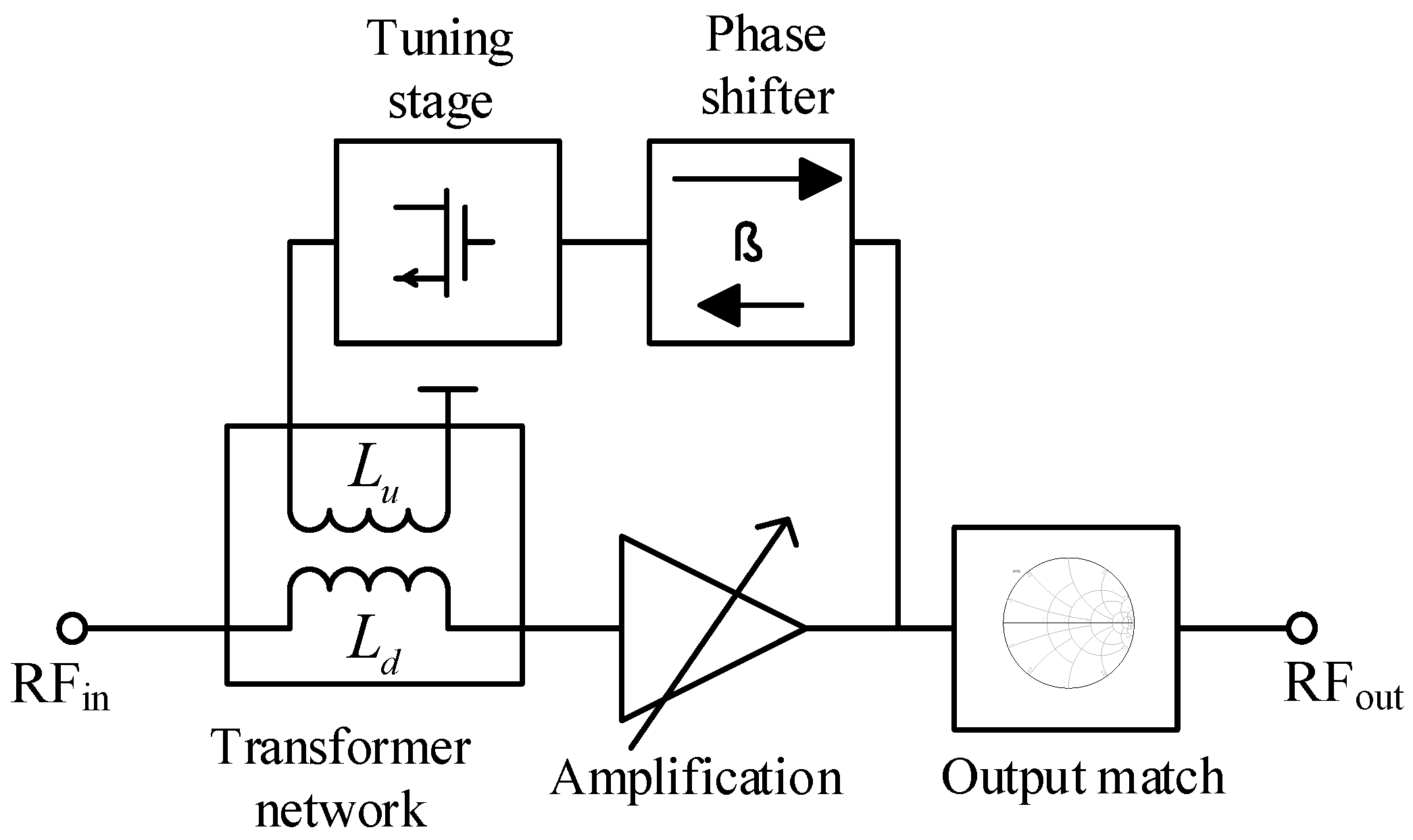
Figure 2 shows the block representation of the proposed CTLNA which consists of four different stages. The first stage is the input matching stage that consists of an input capacitor C1 and a physical transformer. The second stage consists of a phase shifter network that comprises of two CG transistors connected in parallel to a CS transistor to get a relative 0° or 180° phase shift between the currents through primary and the secondary windings of the transformer. The third stage consists of tuning transistor whose bias voltage Vtune can be varied to get the desired tunability. Finally, the fourth stage is the amplification stage that achieves a tunable wideband gain when Vtune is varied. For better understanding of the proposed circuit topology, design and synthesis of each stage is described as follows.
3.1. Transformer Network
The transformer in the input stage is an RF impedance transformer. One end of its primary winding Lu is connected to the output of tuning transistor, while the other end is connected to the voltage supply VDD2 = 1.3 V. The secondary winding Ld is connected to the input transistor via a DC bias network. If Ld is considered as a variable inductor as shown in Figure 2, then scaling its value will provide a 50 Ω impedance matching at different center frequencies. The design utilizes a similar concept by implementing an RF impedance transformer in place of a variable inductor. Therefore, frequency reconfigurability can be achieved if current passing through Ld can be changed. The magnetism property of transformer can be utilized [22] to change current through Ld. However, the currents i1 and i2 through Lu and Ld must have a relative phase shift ϕ of either 0° or 180° to allow continuous frequency tunability. This is because the RF impedance transformer circuit, shown in Figure 3a, provides a 50 Ω impedance match at a phase difference of 0° or 180° and the impedance is purely real at ϕ = 0°.This can be substantiated by deriving the relationship between transformer’s input impedance and . From the simplified transformer network shown in Figure 3b and can be given as
Inverting Equation (7) and substituting s = jω, is
where is the ratio of primary and secondary winding currents in the transformer network, M is the mutual inductance, is primary leakage, is interwinding capacitance and is core loss resistance. Inductances and correspond to inductances and in the implemented transformer network and given as.
where k is the coefficient of coupling and N is the turns ratio. Due to phase difference between and , where is the gain and [22]. Therefore, Equation (8) can be expanded as
Substituting values for variables in Equation (11) as Rc = 0.91 Ω, β = 1, ω = 2πf, f = 3 GHz, Lt1 = 3.37 nH, M = 0.5 nH, C = 995 fF and plotting vs. from 0° to 360°, we can verify that = 50 Ω at 0° and 180° as shown in Figure 4a, despite the fact that our transformer model is different to that in [22].
Additionally, is maximum at ϕ = 180° which leads to a phase mismatch between i1 and i2; however, the desired relative phase shift between i1 and i2 is 0° for continuous tuning. Moreover, the amplified signal is an inverted version of input signal. A possible solution is a phase shifter circuit that can provide a phase mismatch of 0° to ensure that currents and are in phase. The resonant frequency of transformer can be determined as
The transformer’s coefficient of coupling k is related to M as . A lower value of k would result in lower M and less sensitivity of transformer network to large frequency variation and current mismatch. Therefore, the value of k was kept low to achieve the desirable input match. Table 1 summarizes the design parameters for the transformer network.
3.2. Phase Shifter
The circuit implements a conventional active phase shifter (APS) [23] to shift the phase of the amplified signal. The APS receives the amplifier output and is applied in the feedback path of the circuit. The circuit embeds two CG transistors in parallel to a CS transistor. Figure 5a shows the schematic of adapted APS circuit with a conventional topology. The designed circuit is capable of providing a phase shift of more than 90°, thereby leading to elimination of phase mismatch between complex currents and . A simplified small signal equivalent circuit to illustrate the conventional APS operation is shown in Figure 5b. According to [23], in admittance matrix for the APS is given as:
Transformation of to can be expressed as
From Equation (14), the phase of can be derived as
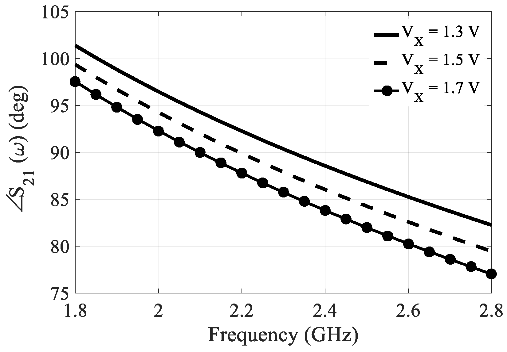
where and are the input impedance and the output impedance of APS, respectively. It can be concluded from Equation (15) that phase of S21(ω) depends upon inductor Lp and capacitor Cp. The shift in phase of the signal with constant signal amplitude is accomplished by variation in inductance or capacitance of the resonant circuit. The values of Lp and Cp for 2.2 to 2.8 GHz band are 17.5 nH and 10 pF, respectively. Figure 6 shows variation of phase of S21(ω) of APS with VX. The circuit provides a more than 90° phase shift in our desired frequency range.
3.3. Tuning Stage
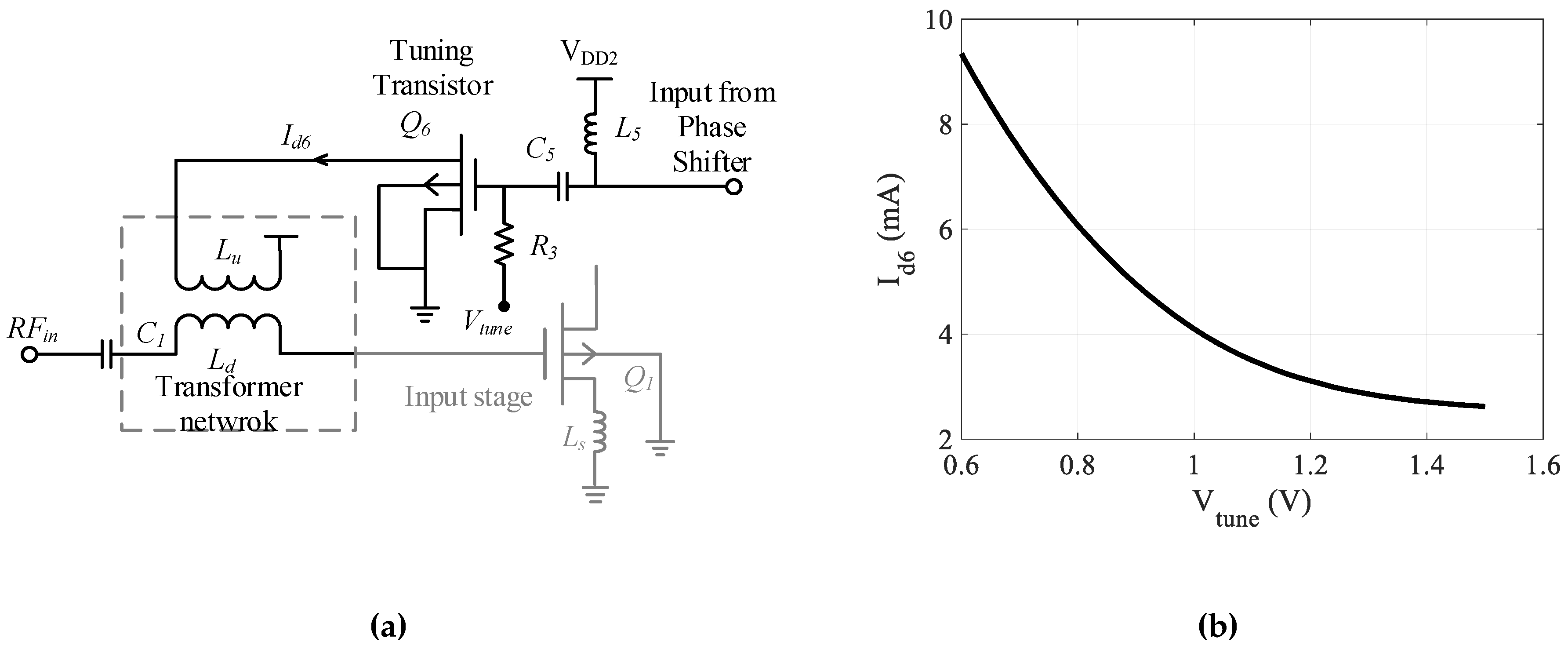
Figure 7a shows the tuning stage of the designed CTLNA. It consists of a CS transistor biased with a positive gate voltage through a bias resistor. The CS transistor is placed in the feedback path and the input to its gate terminal is a phase shifted signal from the output of APS circuit. The output drain terminal is connected to one end of primary winding Lu of transformer network in the input stage. Varying the bias voltage () of tuning transistor Q6 continuously leads to incessant variation in its drain current . This further leads to variation in current flowing through and resultantly in α and β. Figure 7b shows the variation of with . The resultant change in (depends on β) varies the input impedance of CTLNA, leading to continuous tunability.
4. Circuit Analysis
Figure 8 shows the complete architecture of designed CTLNA with source degeneration and cascode topology. The cascode topology increases the circuit’s AC resistance and aids in augmenting the gain. Inductive degeneration increases the real part of input impedance. The primary consideration while designing a CTLNA is to determine the band of operation. Ct, Lp and k values in transformer network are then selected to focus the desired operating band that ranges from 2.2 GHz to 2.8 GHz. One end of primary winding of the transformer in input stage is terminated with output from the tuning transistor, while the other end is connected to voltage supply. Input capacitor C1 resonates with Ld to achieve a continuously tunable impedance matching at different center frequencies. Continuous tuning shall only take place when and are in phase. The input of APS circuit is connected to the drain of Q1 via L3–C3 network. It provides a phase mismatch of 0° between the currents and through Lu and Ld. The output of APS is fed to gate of Q6 whose drain terminal further connects to Lu to achieve tunable input matching.
A resistance is also added for the purpose of providing DC bias to the input transistor Q1. For simplicity, a fixed inductor was adopted in the output loading section of LNA to achieve a wideband gain. A large resistance is added in parallel to for improving LNA stability at different frequencies and DC voltage gain.
4.1. Input Impedance
The input stage of the proposed CTLNA consists of capacitor C1 and the transformer network. Secondary inductor Ld can be considered as a tunable inductor that replaces Lg in Figure 1 to achieve tunable input impedance. As Ld cannot be directly varied, magnetic coupling can be utilised to vary the input impedance of LNA. Since depends on α, the input impedance of CTLNA in Figure 8 is derived as
where Cx is equivalent capacitance of and C1. Equation (17) shows that depends on constants Ld, Ls, M, and variable α. The value of α can be varied by changing that controls and . Note that the real part of input impedance depends on Ls and can be changed by varying Ls only. Its value has been selected to ensure that is matched to the source. The quality factor of input matching network is one of the primary elements used to determine the bandwidth of network. For the designed CTLNA, can be expressed as
where and R are imaginary and real part of input impedance, respectively. From (17) and (18), can be simplified as
It can be concluded from (19) that the bandwidth and of CTLNA increases as Qin becomes smaller.
4.2. Gain
Gain of designed CTLNA can be derived similar to a narrowband LNA shown in Figure 1. However, in this case, the input gate inductor Lg is replaced with a transformer based variable inductor Ld and its impedance depends on M and α. The output loading network is similar to a conventional load. The low noise voltage gain for CTLNA can be derived from its small signal model of input and amplification stage shown in Figure 9. For cascode LNAs, since all transistors are the same,
where is conduction parameter, is the transconductance of the transistor Q2 and is the threshold voltage of implemented Philips MOS transistor. The small signal voltage gain of an LNA is defined as
Substituting Equation (16) in Equation (23), Vin expands to
Also,
From Equations (22) and (25),
Finally, substituting Equations (24) and (26) in Equation (21), can be derived as
where is the gate-source capacitance of the transistor Q2. Equation (27) substantiates that for the designed CTLNA depends on α and eventually on . Hence the gain can also be tuned continuously in the desired band by sweeping from 0.5 V to 1.5 V.
4.3. Noise Figure
Figure 10 shows the noise equivalent model for the designed circuit. NF for the proposed CTLNA can be quantified by deriving its noise factor F. The main noise source in the circuit is thermal noise and all passives in the circuit are considered as ideal. Considering that there are multiple noise sources in the circuit, it would be rather impractical to evaluate F without detailed noise model for all noise sources. Therefore, an expression for output noise current due to all noise sources is calculated. The short circuit noise current due to source is
and
where and , is the zero introduced due to noise effect from other transistors Q2, Q3 and Q4 in parallel and is the noise voltage at source. The short circuit noise current due to thermal drain noise of transistor Q1, Q2 in amplification stage is
where and are drain noise currents of Q1 and Q2. The transistors Q3, Q4 and Q5 in the PS circuit also contribute to the overall NF of CTLNA. Therefore, short circuit noise current due to drain noise of Q3, Q4 and Q5 is
The short-circuit noise current due to drain noise of tuning transistor Q6 is
and due to load is
where , , , are the noise currents of transistors Q3, Q4, Q5 and Q6 and is the noise current of load resistance RL. Using (28) to (33), F for the proposed LNA can be derived as
5. Results and Discussion
The proposed CTLNA is designed and simulated in MIC process. Keysight ADS and MATLAB are used as simulation tools for CTLNA analysis. The circuit is biased with 1.8 V supply and sinks 9 mA current. As can be seen in Figure 11a, S11 achieves a peak minimum for all different values of from 0.5 V to 1.5 V in steps of 0.2 V. It is below −10 dB at each center frequency for the entire tuning range and achieves as low as −40.4 dB at 2.57 GHz at = 1.2 V.
The LNA input matching network has been designed to match to 50 Ω at a particular centre frequency in the tuning range. The calculated 3 dB bandwidth at 2.2 GHz, 2.3 GHz, 2.41 GHz, 2.52 GHz and 2.65 GHz are 20 MHz, 100 MHz, 10 MHz, 10 MHz and 30 MHz, respectively.
Figure 11b shows simulated gain for the designed CTLNA. The LNA gain directly depends on value of loading inductor L2. However, due to its dependency on it can be tuned to different frequencies from 2.2 to 2.8 GHz. In addition, the CTLNA gain depends upon , , source degeneration inductor , and designed transformer parameters. The LNA achieves a maximum gain of 18 dB at 2.36 GHz in the stipulated tuning range. The minimum gain at 2.2 GHz center frequency is approximately 8 dB. Transistors Q7 and Q8 in the buffer stage are capable enough to stabilize the LNA and achieve high output impedance.
The output return loss S22 is less than -8dB in the tuning range and achieves a peak minimum at center frequency of 2.35 GHz, which is the resonant frequency of output matching network. The reverse isolation S12 also remains more than 30dB across the tuning range. Figure 11c shows the variation of S12 and S22 with frequencies of selected band.
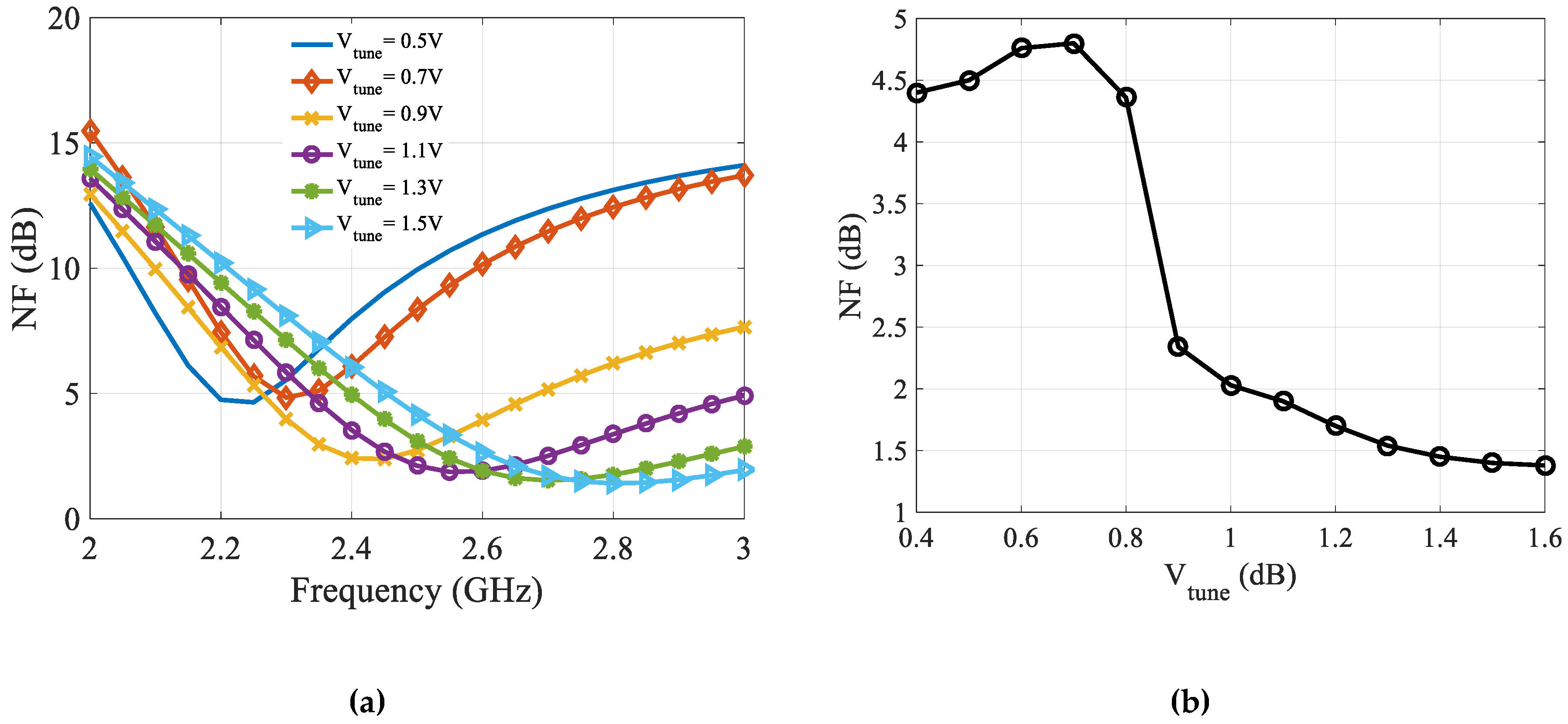
Figure 12a,b show simulated NF for designed CTLNA with tuning frequency and Vtune, respectively. It is clear from Figure 12b that minimum NF at each center frequency varies between 1.4 dB to 4.8 dB. NF is a bit higher for 2.2 GHz and 2.3 GHz, which are initial frequencies in the tuning range. However, it is lower than 2 dB at center frequencies ranging from 2.4 GHz to 2.8 GHz.
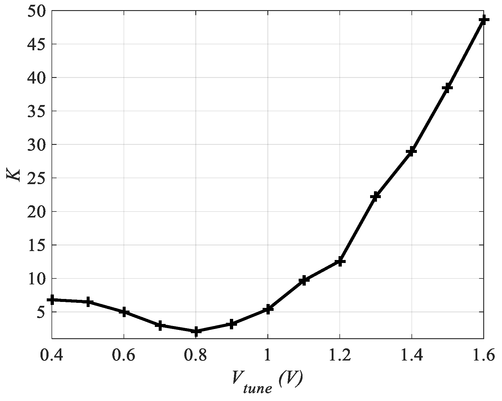
The LNA stability depends upon the source and the load matching networks, which depends on the frequency of operation. Consequently, the designed CTLNA is supposed to be stable at a particular center frequency while it is unstable at other frequencies. Stability of LNA can be determined by calculating stability factor K and stability constant Δ or by plotting stability circles. K and Δ are can be mathematically determined using either Rollet’s criteria or Tan’s formulae [24] as:
For the designed LNA, K > 1 and |Δ| < 1 at all center frequencies within in the tuning range. Kt > 1 is a single variable criterion to determine the unconditional stability of LNA [24]. Subsequently, the LNA is stable in the entire tuning range. Figure 13 shows variation of K with Vtune at different center frequencies.
Linearity of LNA is commonly measured by determining 1-dB compression point P1dB and third-order intercept point IP3. Non-linearities in the system lead to gain-compression that causes the LNA gain to deviate from the normal curve. P1dB and IIP3 calculations have been performed using 1-tone and 2-tone inputs, respectively. A non-linear model of the amplifier is analyzed with a frequency offset of 10 MHz between two tones. The source and load impedances have been set to 50 Ω, while the harmonic frequency was selected to be 2.4 GHz. IP3 and P1dB values for the designed CTLNA, range between −15 dBm to −31 dBm and −25 dBm to −42 dBm, respectively. Figure 14 shows the variation of P1dB with Vtune in steps of 0.1V for the proposed CTLNA.
6. Conclusions
The design and analysis of an input tuning LNA with transformer based variable inductor matching is presented. The proposed CTLNA can be primarily used for SDR applications, such as green radio networks. The presented design takes advantage of continuous tuning due to magnetic coupling between primary and secondary windings of transformer. This occurs by changing the ratio of currents through primary and secondary windings of the transformer network. To achieve tunability, currents through transformer windings should be in phase. The methodology can be used to further implement a tunable LNA along the frequency band of 2.2 to 2.8 GHz. The design effectively integrates the matching network into an inductively degenerated CS amplifier. The LNA achieves a wideband and tunable gain in the stipulated bandwidth. The input return loss is less than −10 dB and achieves a minimum of −40.4 dB at 2.57 GHz. The NF ranges between 1.4 to 4.8 dB. In addition, mathematical analysis of transformer model, phase shifter and amplification stage are discussed. The proposed technique outlines an idea of continuous tuning that can be implemented to scale the input inductor value for any related application. Table 2 summarizes the simulated performance of designed CTLNA and comparison with previously published works.
Author Contributions
Supervision, X.J.L.; conceptualization, A.A. and X.J.L.; formal analysis, A.A.; investigation, A.A.; methodology, A.A. and X.J.L.; writing, A.A. and X.J.L.
Funding
This research received no external funding.
Conflicts of Interest
The authors declare no conflict of interest.
References
- Bazrafshan, A.; Taherzadeh-Sani, M.; Nabki, F. A 0.8–4-GHz Software-Defined Radio Receiver With Improved Harmonic Rejection Through Non-Overlapped Clocking. IEEE Trans. Circuits Syst. I Regul. Pap. 2018, 65, 3186–3195. [Google Scholar] [CrossRef]
- Adom-Bamfi, G.; Entesari, K. A multiband low noise amplifier with a switchable Gm active shunt feedback for SDRs. In Proceedings of the IEEE Radio and Wireless Symposium (RWS), Austin, TX, USA, 24–27 January 2016; pp. 179–182. [Google Scholar]
- Aneja, A.; Li, X.J.; Li, B.E. Design of Continuously Tunable Low Noise Amplifier for Multiband Radio. In Proceedings of the 2017 Mediterranean Microwave Symposium (MMS), Marseille, France, 28–30 November 2017; pp. 1–4. [Google Scholar]
- Yu, X.; Neihart, N.M. A 2–11 GHz reconfigurable multi-mode LNA in 0.13 µm CMOS. In Proceedings of the IEEE Radio Frequency Integrated Circuits Symposium (RFIC), Montreal, QC, Canada, 17–19 June 2012; pp. 475–478. [Google Scholar]
- El-Nozahi, M.; Sanchez-Sinencio, E.; Entesari, K. A CMOS low-noise amplifier with reconfigurable input matching network. IEEE Trans. Microw. Theory Tech. 2009, 57, 1054–1062. [Google Scholar] [CrossRef]
- Wu, C.-R.; Hsieh, H.-H.; Lai, L.-S.; Lu, L.-H. A 3–5 GHz frequency-tunable receiver frontend for multiband applications. IEEE Microw. Wirel. Compon. Lett. 2008, 18, 638–640. [Google Scholar] [CrossRef]
- Kwon, K.; Kim, S.; Son, K.Y. A Hybrid Transformer-Based CMOS Duplexer With a Single-Ended Notch-Filtered LNA for Highly Integrated Tunable RF Front-Ends. IEEE Microw. Wirel. Compon. Lett. 2018, 28, 1032–1034. [Google Scholar] [CrossRef]
- Wang, J.-J.; Chen, D.-Y.; Wang, S.-F.; Wei, R.-S. A multi-band low noise amplifier with wide-band interference rejection improvement. AEU-Int. J. Electron. Commun. 2016, 70, 320–325. [Google Scholar] [CrossRef]
- Zokaei, A.; Amirabadi, A. A dual-band common-gate LNA using active post distortion for mobile WiMAX. Microelectron. J. 2014, 45, 921–929. [Google Scholar] [CrossRef]
- Neihart, N.M.; Brown, J.; Yu, X. A dual-band 2.45/6 GHz CMOS LNA utilizing a dual-resonant transformer-based matching network. IEEE Trans. Circuits Syst. I Regul. Pap. 2012, 59, 1743–1751. [Google Scholar] [CrossRef]
- Yu, X.; Neihart, N.M. Analysis and design of a reconfigurable multimode low-noise amplifier utilizing a multitap transformer. IEEE Trans. Microw. Theory Tech. 2013, 61, 1236–1246. [Google Scholar] [CrossRef]
- Fu, C.-T.; Ko, C.-L.; Kuo, C.-N.; Juang, Y.-Z. A 2.4–5.4-GHz wide tuning-range CMOS reconfigurable low-noise amplifier. IEEE Trans. Microw. Theory Tech. 2008, 56, 2754–2763. [Google Scholar]
- Kia, H.B.; A’ain, A.K.; Grout, I.; Kamisian, I. A reconfigurable low-noise amplifier using a tunable active inductor for multistandard receivers. CircuitsSyst. Signal Process. 2013, 32, 979–992. [Google Scholar] [CrossRef]
- Wu, C.-R.; Lu, L.-H. A 2.9-3.5-GHz tunable low-noise amplifier. In Proceedings of the IEEE Topical Meeting on Silicon Monolithic Integrated Circuits in RF Systems, San Diego, CA, USA, 18–20 January 2006. [Google Scholar]
- Beare, R.; Plett, C.; Rogers, J. Highly reconfigurable single-ended low noise amplifier for software defined radio applications. In Proceedings of the IEEE 10th International New Circuits and Systems Conference (NEWCAS), Montreal, QC, Canada, 17–20 June 2012; pp. 549–552. [Google Scholar]
- Chen, Z.; Zhang, X.; Song, Z.; Jia, W.; Chi, B. A 1.0–5.0 GHz tunable LNA with automatic frequency calibration in 65 nm CMOS. In Proceedings of the 2016 IEEE International Symposium on Radio-Frequency Integration Technology (RFIT), Taipei, Taiwan, 24–26 August 2016; pp. 1–3. [Google Scholar]
- Emami, N.; Arshed, O.; Bakri-Kassem, M.; Albasha, L. Reconfigurable low noise amplifier using MEMS varactor. In Proceedings of the 2013 8th International Conference on Design & Technology of Integrated Systems in Nanoscale Era (DTIS), Abu Dhabi, UAE, 26–28 March 2013; pp. 145–150. [Google Scholar]
- Akbar, F.; Atarodi, M.; Saeedi, S. Design method for a reconfigurable CMOS LNA with input tuning and active balun. AEU-Int. J. Electron. Commun. 2015, 69, 424–431. [Google Scholar] [CrossRef]
- Macias-Bobadilla, G.; Rodríguez-Reséndiz, J.; Mota-Valtierra, G.; Soto-Zarazúa, G.; Méndez-Loyola, M.; Garduño-Aparicio, M. Dual-Phase Lock-In Amplifier Based on FPGA for Low-Frequencies Experiments. Sensors 2016, 16, 379. [Google Scholar] [CrossRef]
- Brown, J. Design of a Magnetically Tunable Low Noise Amplifier in 0.13 um CMOS Technology; Iowa State University: Ames, IA, USA, 2012. [Google Scholar]
- Gómez-Espinosa, A.; Hernández-Guzmán, V.M.; Bandala-Sánchez, M.; Jiménez-Hernández, H.; Rivas-Araiza, E.A.; Rodríguez-Reséndiz, J.; Herrera-Ruíz, G. A New Adaptive Self-Tuning Fourier Coefficients Algorithm for Periodic Torque Ripple Minimization in Permanent Magnet Synchronous Motors (PMSM). Sensors 2013, 13, 3831–3847. [Google Scholar] [CrossRef] [PubMed] [Green Version]
- Brown, J.L.; Neihart, N.M. An analytical study of a magnetically tuned matching network. In Proceedings of the IEEE International Symposium on Circuits and Systems (ISCAS), Seoul, Korea, 20–23 May 2012; pp. 1979–1982. [Google Scholar]
- Hayashi, H.; Mauraguchi, M. An MMIC active phase shifter using a variable resonant circuit [and MESFETs]. IEEE Trans. Microw. Theory Tech. 1999, 47, 2021–2026. [Google Scholar] [CrossRef]
- Tan, E.L. A quasi-invariant single-parameter criterion for linear two-port unconditional stability. IEEE Microw. Wirel. Compon. Lett. 2004, 14, 487–489. [Google Scholar] [CrossRef]
Figure 1.
(a) Conceptual representation of a conventional input tuning LNA with Lg (b) Corresponding varying S11 for different values of Lg. (c) Small signal equivalent of conventional LNA.
Figure 1.
(a) Conceptual representation of a conventional input tuning LNA with Lg (b) Corresponding varying S11 for different values of Lg. (c) Small signal equivalent of conventional LNA.

Figure 2.
Conceptual block of proposed CTLNA.

Figure 3.
(a) Physical transformer equivalent circuit for designed CTLNA (b) simplified transformer model for calculations.
Figure 3.
(a) Physical transformer equivalent circuit for designed CTLNA (b) simplified transformer model for calculations.
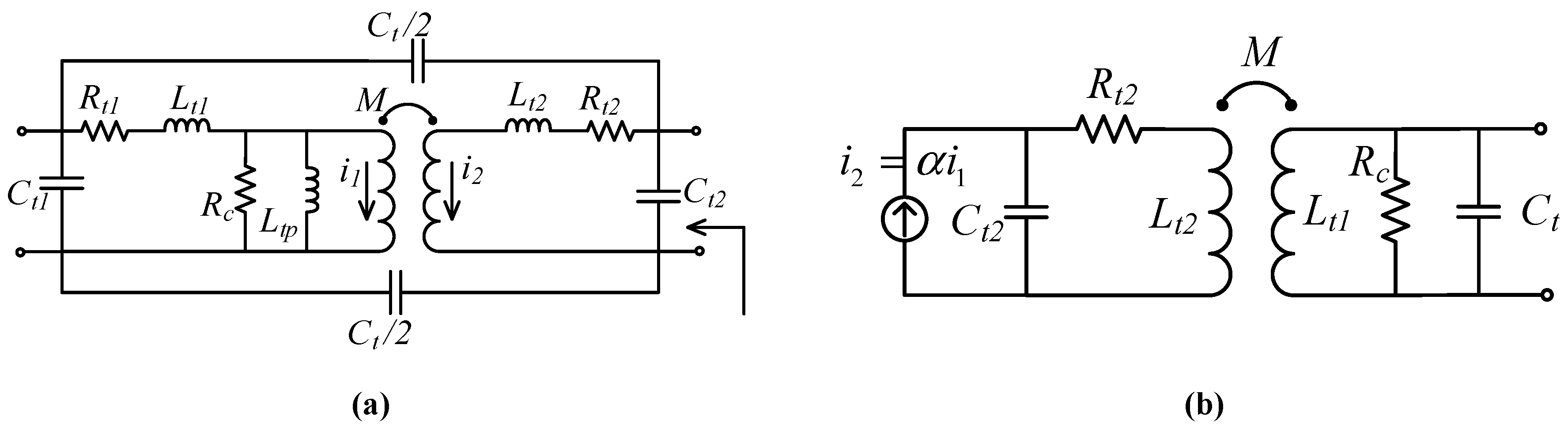
Figure 4.
(a) , (b) as a function of .

Figure 5.
(a) Implemented PS circuit, (b) equivalent small signal model [23].
Figure 5.
(a) Implemented PS circuit, (b) equivalent small signal model [23].
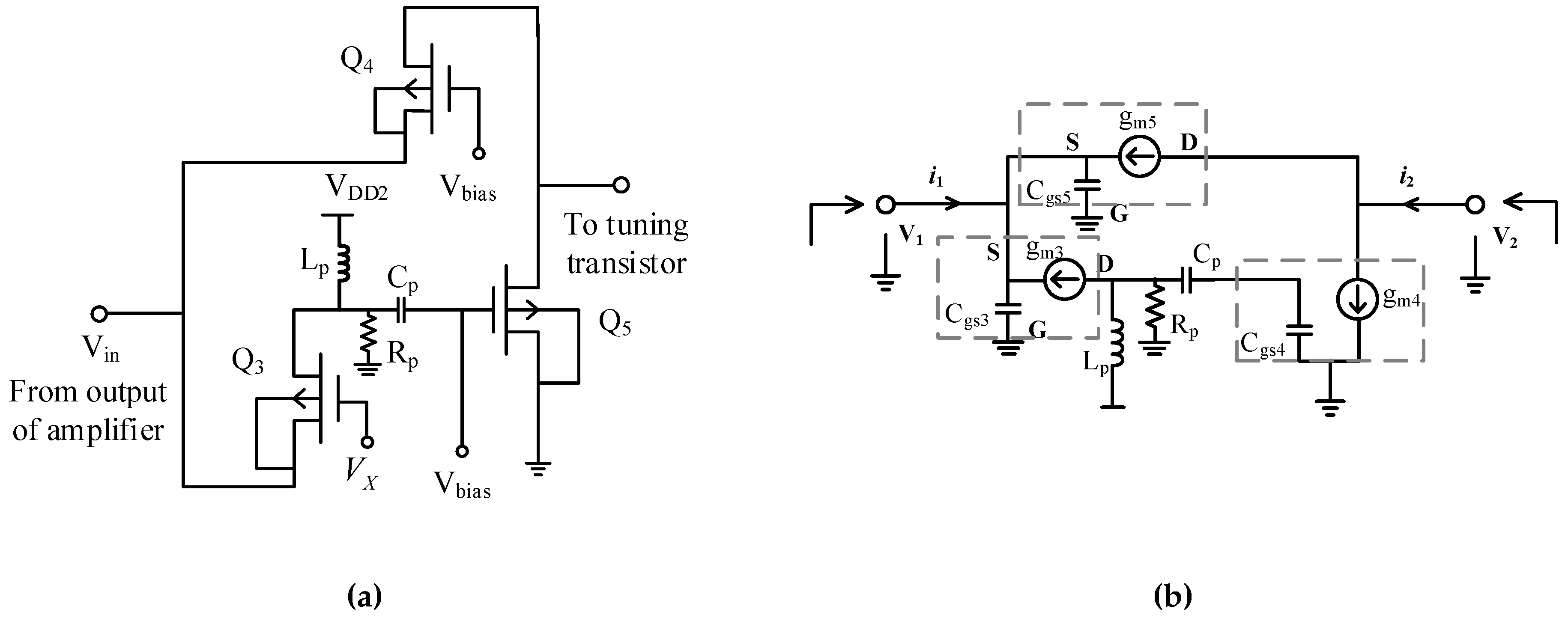
Figure 6.
Frequency at different values of .

Figure 7.
(a) Tuning stage of proposed CTLNA (b) variation of with .

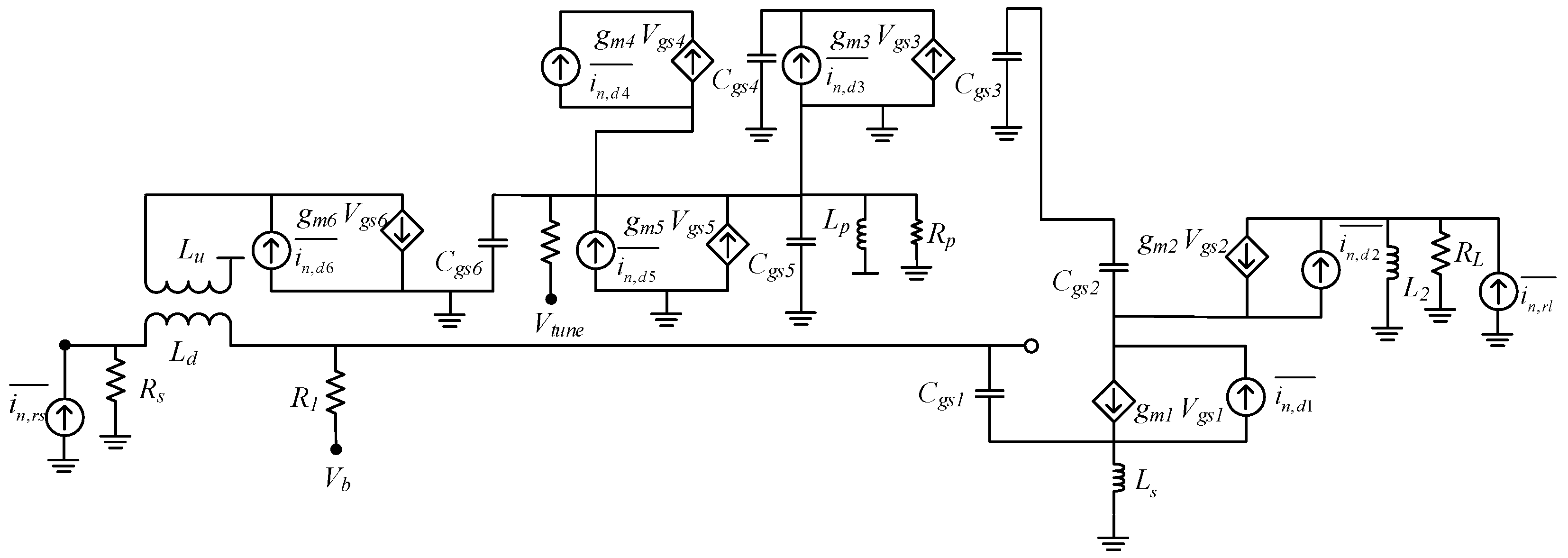
Figure 8.
Complete CTLNA architecture.
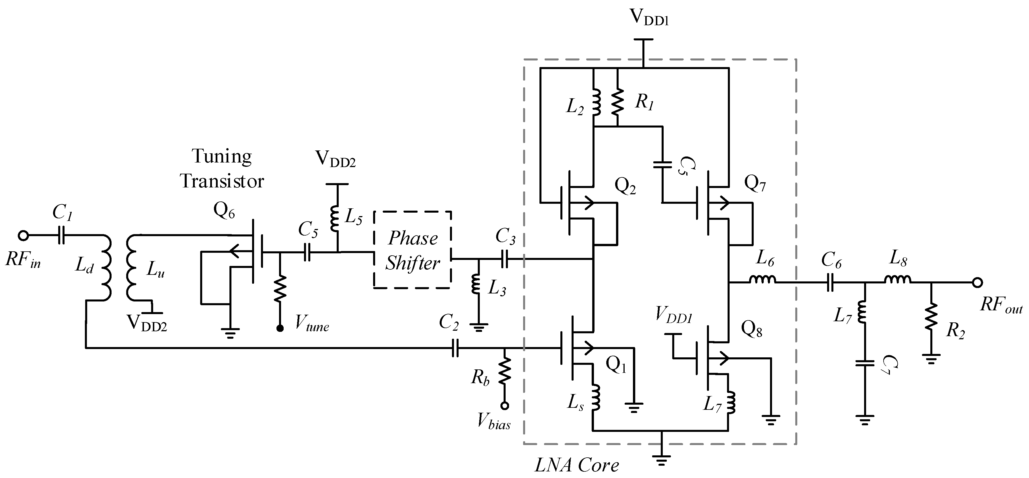
Figure 9.
Simplified small signal model of CTLNA for gain analysis.
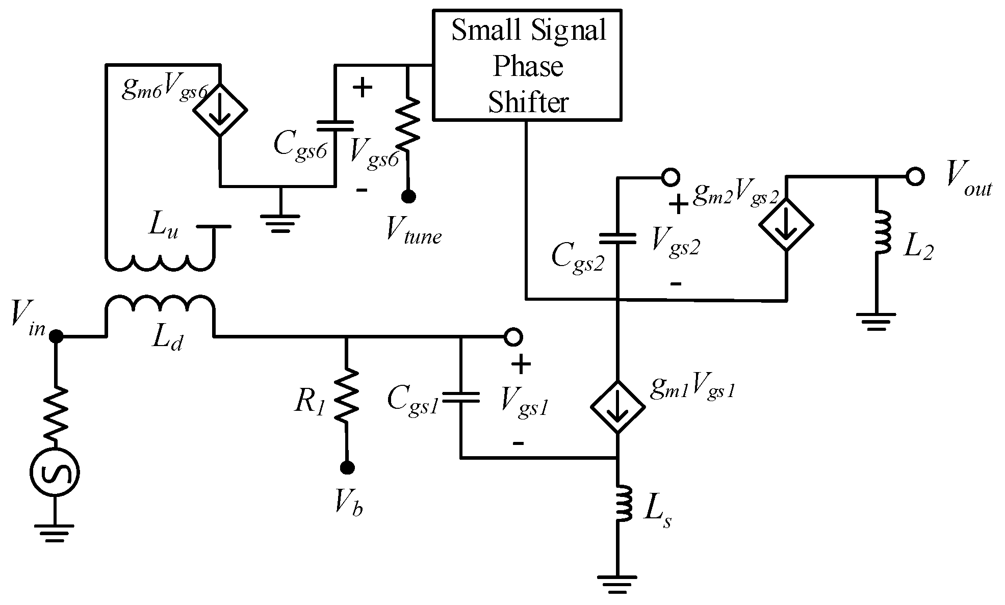
Figure 10.
Noise equivalent model of designed CTLNA.

Figure 11.
Simulated (a) input return loss (S11) (b) Gain (S21) (c) Reverse isolation (S12) and output return loss (S22).
Figure 11.
Simulated (a) input return loss (S11) (b) Gain (S21) (c) Reverse isolation (S12) and output return loss (S22).
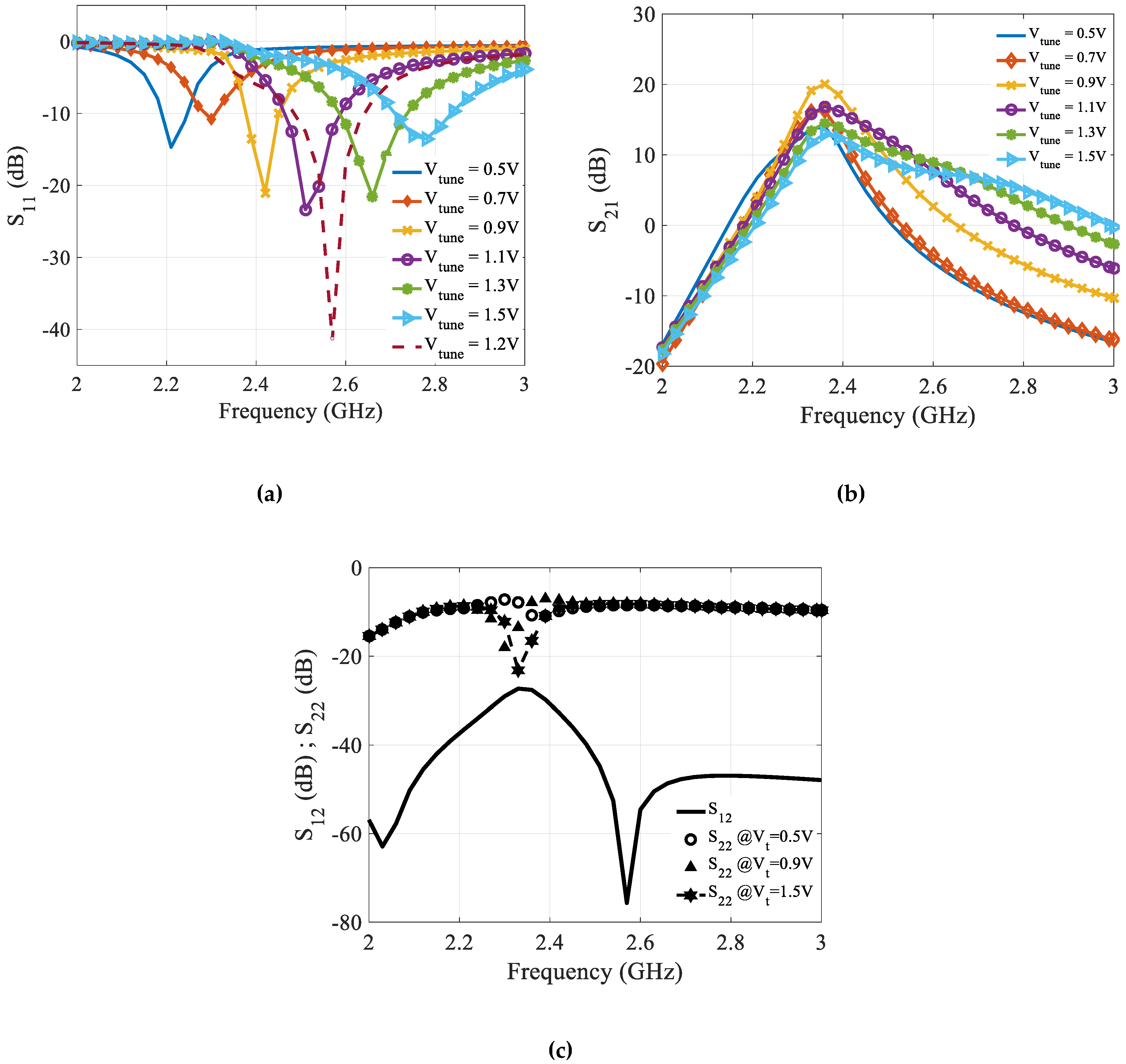
Figure 12.
Simulated NF vs. (a) Frequency (b) Vtune.

Figure 13.
Variation of Stability factor K with Vtune.

Figure 14.
Variation of P1dB with Vtune.


Table 1.
Transformer design parameters.
| Parameter | Value |
|---|---|
| Turns Ratio ‘N’ | 0.69 |
| Magnetising Inductance ‘Ltp’ | 2.23 nH |
| Cross loss resistance ‘Rc’ | 1000 |
| Coefficient of Coupling ‘k’ | 0.11 |
| Primary loss resistance ‘Rt1’ | 0.91 |
| Secondary loss resistance ‘Rt2’ | 4.47 |
| Primary capacitance ‘Ct1’ | 924 fF |
| Secondary capacitance ‘Ct2’ | 150 fF |
| Interwinding capacitance ‘Ct’ | 340 fF |
Table 2.
CTLNA performance summary and comparison with previously published works.
| Ref. | Freq. (GHz) | S21 (dB) | S11 (dB) | NF (dB) | IP3 (dBm) | VDD | Tech. | PDC (mW) |
|---|---|---|---|---|---|---|---|---|
| This work | 2.2–2.8 | 7–18 | −40–−11 | 1.4–4.8 | −31–15 | 1.8 | MIC | 16.2 |
| [16] | 1–5 | 19–27 | −18–−5 | 2.4–3.8 | - | 1.2 | 65 nm CMOS | 12.1 |
| [5] | 1.9–2.4 | 10–14 | −25–12 | 3.2–3.7 | −6.7 | 1.2 | 0.13 µm CMOS | 17 |
| [12] | 2.4–5.4 | 9.9–22 | −14–−30 | 2.4–4.9 | −20.4–−9.7 | 1 | 0.13 µm CMOS | 3.1–4.6 |
| [13] | 0.8–2.5 | 17–20 | −27–−11 | 3.1–3.6 | - | 1.8 | 0.18 µm CMOS |
© 2019 by the authors. Licensee MDPI, Basel, Switzerland. This article is an open access article distributed under the terms and conditions of the Creative Commons Attribution (CC BY) license (http://creativecommons.org/licenses/by/4.0/).
Share and Cite
MDPI and ACS Style
Aneja, A.; Li, X.J. Design and Analysis of a Continuously Tunable Low Noise Amplifier for Software Defined Radio. Sensors 2019, 19, 1273. https://doi.org/10.3390/s19061273
AMA Style
Aneja A, Li XJ. Design and Analysis of a Continuously Tunable Low Noise Amplifier for Software Defined Radio. Sensors. 2019; 19(6):1273. https://doi.org/10.3390/s19061273
Chicago/Turabian StyleAneja, Aayush, and Xue Jun Li. 2019. "Design and Analysis of a Continuously Tunable Low Noise Amplifier for Software Defined Radio" Sensors 19, no. 6: 1273. https://doi.org/10.3390/s19061273
Note that from the first issue of 2016, this journal uses article numbers instead of page numbers. See further details here.