Introduction
The advances in sensor technologies, including Micro-Electro-Mechanical Systems (MEMS), and associated interfaces, signal processing and networking have made it possible to construct highly functional “smart” sensors and to connect a large number of sensors for distributed measurement and control applications. The networking of many smart sensors enables high quality detection/measurement networks with low cost and easy deployment, and it provides new monitoring and control capability for a wide range of applications, such as industrial process monitoring, health care, environmental oversight, safety and security.
In a sensor network, sensors are generally connected to a microcontroller which provides built-in linearization, error correction, and the access to the network. The interface between the sensor node and the microcontroller becomes important to achieve easy deployment, low power, low cost, and high reliability. Some digital interfaces which were not originally designed for sensor networks, such as I2C and RS-232, have been widely used in the industry. However, some specific characteristics of the sensor network require more features for the interface. Energy efficiency may be of importance if thousands of nodes operate unattended for a long period of time. In some applications the configuration of the system needs to be done automatically and, therefore, plug-n-play, hot swap functions become necessary for the sensor network. The interface between the sensor and the microcontroller should be carefully chosen to meet the requirements of the application.
To provide a guideline for choosing the appropriate bus for different applications, this paper will review the existing digital communication buses, including I2C, SPI, IEEE1451.2, and IEEE1451.3, which can be used for sensor networks. Several architectures for sensor networks will then be presented. A new sensor bus for hardwired intra-module communication will then be presented. Finally, some issues in the wireless sensor networking will be discussed.
Sensor Bus Standards
A sensor usually imposes very moderate requirements on the communication rate and hardware complexity. A serial bus structure is the most efficient realization among different bus structures. It can provides the minimum number of interconnects in the sensor network and also achieve low cost and high reliability [
1]. A serial bus is therefore generally used in a smart sensor system. This section will discuss the digital interface between the microcontroller and smart sensors, including some general serial buses as well as buses which are designed specifically for sensor networks.
Inter-IC Bus
The Inter-IC (I
2C) bus [
2] was introduced by Philips Semiconductor as a standard for connecting networked integrated circuits which may or may not include sensors. I
2C is intended for application in systems which connect microcontrollers and other microcontroller-based peripheral devices. It is a two wire serial bus to minimize the cost of connecting the various devices in the system, as shown in
Figure 1. Two wires, serial data and serial clock, carry information between the devices connected to the bus. The serial data wire is bi-directional but data may flow in only one direction at a given time. Each device is identified by a unique address. Devices on the bus are defined as masters or slaves. A master initiates a data transfer on the bus and generates the clock; it also generates the control signals which are placed on the data wire. The slave device is a device which is controlled by the master. A slave can either receive or send data depending on the master.
Master devices are usually microcontrollers. The I2C bus is a multi-master bus. Therefore, more than one microcontroller can be connected to the bus. An arbitration procedure is implemented to avoid the chaos that might ensue from simultaneous data transfer by multiple micro-controllers.
The bus can operate in three modes with different data rates. Data on the bus can be transferred at rates of up to 100kbit/s in the standard-mode, up to 400 kbit/ in the fast-mode, or up to 3.4 Mbit/s in the high-speed mode. The number of interfaces connected to the bus is dependent on the bus capacitance limit of 400pf.
Figure 1.
Typical I2C bus configuration.
Figure 1.
Typical I2C bus configuration.
I2C bus supports two addressing schemes: 7-bit address and 10-bit address. Up to 1024 devices are allowed to be connected to the bus. The 7-bit address scheme has shorter message length and requires less complex hardware. Devices with 7 and 10 bit addresses can be mixed in the same system.
I2C bus allows a system design to rapidly progress directly from a functional block diagram to a prototype. The integrated addressing and data-transfer protocol allow systems to be completely software-defined. The topology is simple and the number of connection wire is minimized. However, although the hardware specification allows for simple interfacing, the communication protocol is rigid. The control signals from the master (such as start condition, stop condition, acknowledge) are encoded on the data wire which increase the required complexity of the interface hardware.
I2C bus does not support plug-n-play or interrupt functions which are important for many sensor networks. To save energy, some sensor nodes should be in sleep mode most of the time and woken up by a timer or sensing event. For each information transport, the microcontroller should initiate the request and provide the clock to the sensors. To get the updated information from the sensor, the microcontroller has to poll each sensor node connected on the bus very often to make sure it will not miss new information or unexpected events. These features make I2C unsuitable for the applications which have strict requirement for the power efficiency and emergency processing. Although the sensor node could be clipped to or from the system easily, the microcontroller can not detect an event or configure the system during operation. This limits the application of I2C in sensor networks which are usually dynamically reconfigurable and/or demand high energy-efficiency.
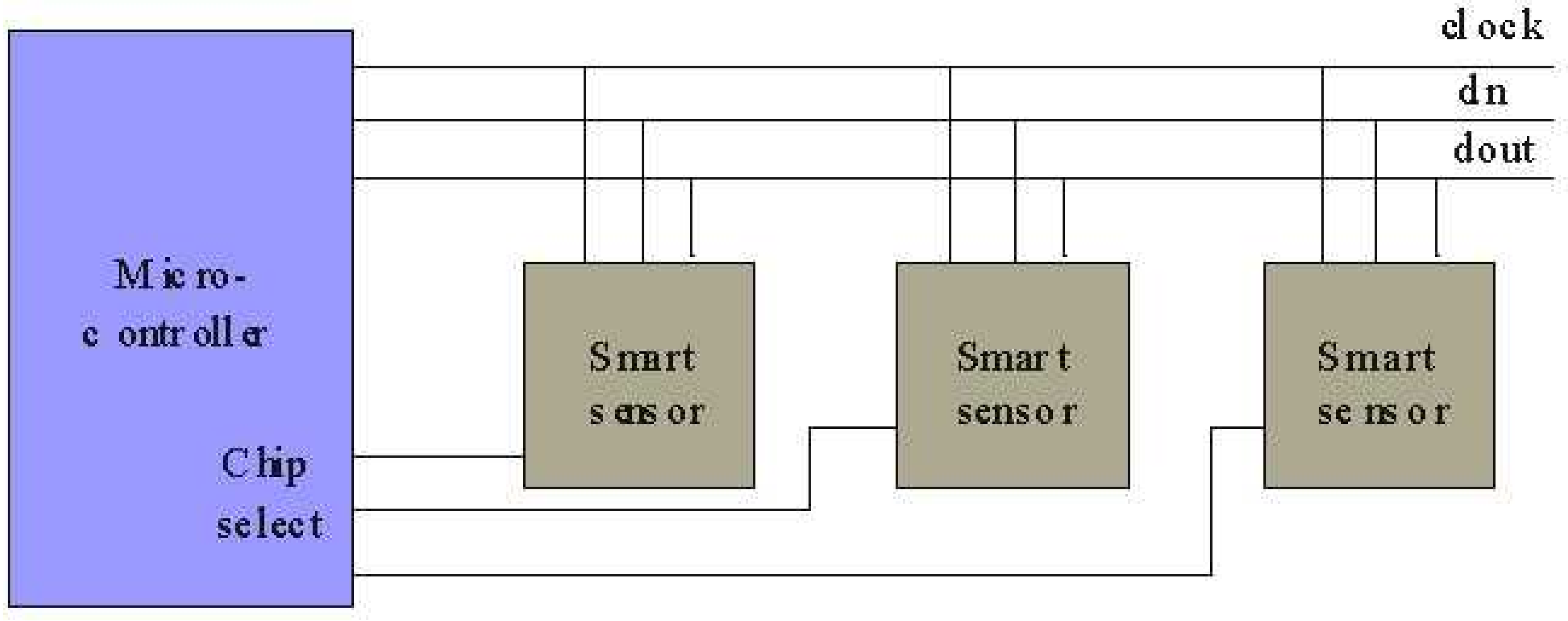
Serial Peripheral Interface
Serial Peripheral Interface (SPI) is a three wire serial bus for 8-bit data transfer applications [
3].
Figure 2 represents a configuration of the SPI bus. Two of the three lines transfer data and the third is the serial clock. Similar to I
2C bus, devices on the bus are defined as masters and slaves. A master initiates an information transfer and generates the clock. Each slave device on the bus is controlled by a chip select line, which is a parallel line for each bus node in addition to the three SPI bus signals.
Figure 2.
Typical SPI bus configuration.
Figure 2.
Typical SPI bus configuration.
The two data lines are unidirectional and the clock signal is generated by the master. The dout line carries data from the master (microcontroller) to the slave (sensor) while din carries data from the slave to the master. The SPI bus employs a simple shift register data transfer scheme. Data transfer is usually performed in eight or sixteen bit blocks. Information on the SPI bus can be transferred at a rate of near zero bits per second to 1 Mbits per second.
Four clock modes are defined for the SPI bus by clock polarity and clock phase settings. The clock polarity determines the level of the clock idle state and the clock phase determines the clock edge that places new data on the bus. Any hardware device capable of operating in more than one mode will have some methods of selecting the value of these mode control settings. This multi-mode capability combined with the simple shift-register architecture makes the SPI bus very versatile and allows many non-serial devices to be used as SPI slaves.
SPI is an attractive bus for smart sensor microsystems. Two separated data lines and the simple shift register data transfer scheme make the hardware of an SPI interface much more simple than that of the I2C bus. However, an individual node enable line is needed to select the device connected on the bus. Since select lines are generally provided by the master (microcontroller), this greatly limits the number of the sensor nodes in the system, and consequently the size of the sensor network. Also, unlike I2C, the SPI bus does not allows new sensors to be easily added to the system without any additional external interfacing. An SPI smart sensor system could not be modified or upgraded simply by “clipping’ or unclipping the sensor to or from the bus without affecting any other circuits on the bus. Finally, as with the I2C bus, SPI has no control signal for new-sensor and/or interrupt detection which makes it unsuitable for many applications including environment monitoring and event detection.
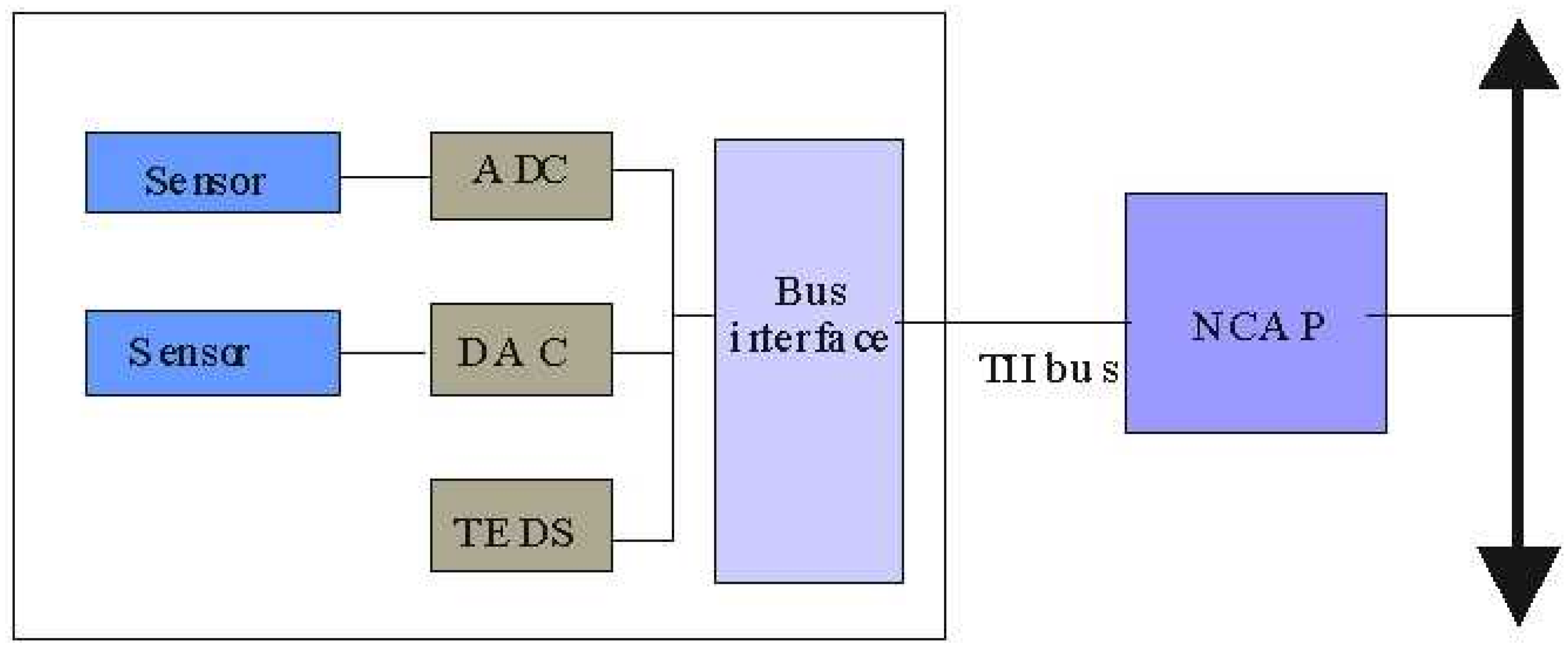
Transducer-Independent Interface
The recently adopted IEEE P1451.2 standard introduced the Transducer-Independent Interface (TII) [
4,
5,
6]. This standard was defined to provide an industry-standard interface to connect sensors to microprocessors. The objective of the standard is to provide a common digital interface between transducers and the network communications nodes, and consequently facilitate the transducer manufacturers to develop smart devices and to interface those devices to networks, systems, and instruments by incorporating existing and emerging sensor and networking technologies. The physical representation of IEEE P1451 standard is shown in
Figure 3.
Figure 3.
Physical representation of IEEE 1451.2.
Figure 3.
Physical representation of IEEE 1451.2.
IEEE P1451.2 defines the interface (the hardware and software blocks) for a networked transducer that does not depend on a specific control network. It introduces the concept of NCAP (Network Capable Application Processor) and STIM (Smart Transducer Interface Module). It defines a TEDS (Transducer Electronic Data Sheet) as an integral part of the STIM, and it defines the TII bus. An objective of IEEE P1451.2 has been to separate the network issues from the transducer issues. The STIM handles the sensor and actuator low-level interface activities. The NCAP handles the network interface and has a dedicated interface port to the STIM. The TEDS contains detailed information about the transducer attached to the STIM, such as calibration coefficients, type of sensor, model number, data units, etc. TII is the port through which the STIM and the NCAP communicate to each other.
IEEE P1451.2 defines sixteen functional addresses. They control the STIM as well as reading and writing both data and memories in the STIM via TII. Certain control and status functions are loosely defined and provisions are available to add vendor unique functions.
TII is a 10-wire digital bus. It is built around synchronous serial communication based on the SPI protocol. Several dedicated lines have been added to provide power, ground and special-purpose control lines, including NIOE, NTRIG, NINT, NSDET and NACK. NIOE is used to indicate the access by the NCAP. NACK toggles after each byte to signal that STIM is ready to continue the data transport frame. NTRIG is an NCAP-generated trigger signal which goes active when the NCAP wants the STIM to take action. The trigger can cause a sensor to take new data or apply previous written data to an output. NINT is the service request or interrupt line. The STIM may use this line to generate an interrupt for a processor. Another feature of the TII bus is that it supports a plug-n-play function. When a STIM is connected to the NCAP, signal line NSDET will go low and the NCAP can detect the condition of the pin and detect the installation or removal of a STIM.
TII is an interface that the sensor manufacturers can use which is independent of the network being used to interconnect the sensors. It provides trigger, interrupt, and plug-n-play functions through dedicated signal lines. The data transport is the same as SPI with 8-bit data words. The software and hardware of the interface are simple, and it can operate with very low power. However, TII allows only one interface module (STIM) to be connected to the microcontroller. It does not support distributed multi-drop sensor modules which are necessary in many sensor network applications. Furthermore, TII needs ten lines between the microcontroller and the sensor module and therefore utilizes considerable controller I/O resources as well as presenting a potential wiring problem.
IEEE P1451.3
IEEE P1451.3 is a proposed standard which attempts to define a set of specifications that will allow a transducer manufacturer to build transducers that have a wide range of price and performance but can interoperate within a system [
7]. It is a multi-drop transducer bus standard, defining a digital interface for connecting multiple, physically separated sensors.
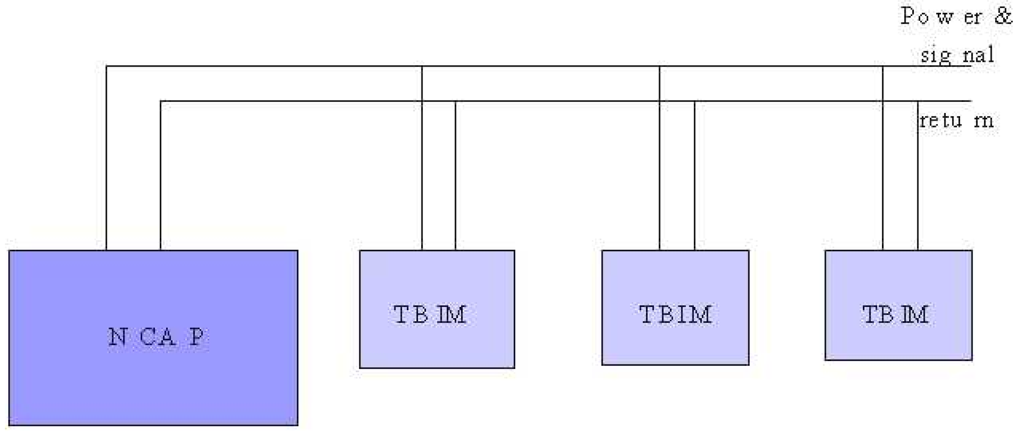
Figure 4 is a representation of what is expected in the physical realm. A single transmission line will be used to supply power to the transducers and to provide the communications between the bus controller and the Transducer Bus Interface Modules (TBIM). A bus is expected to have one bus controller and many TBIMs. As in IEEE P1451.2, the Network Capable Application Processor (NCAP) contains the sensor bus controller as well as interface to the broader network. A TBIM may contain one or more different transducers.
Figure 4.
Physical representation of IEEE1451.3.
Figure 4.
Physical representation of IEEE1451.3.
All TBIMs contains five communication functions, including network communications, TBIM communications, data transfer, synchronization, and triggering. These communication functions will utilize as few as two communications channels on one physical transmission medium. The transmission medium can be a coaxial cable or twisted-pair cable, to five feet or more. The communication channel will share the same signal line as the power supply. For high power transducers, the current that can be supplied over the communications cable may be inadequate, so it will be acceptable to power the transducers with an external power supply. The interface for multiple physically separated modules will support TEDS, as well as channel identification, hot swapping, and time-synchronization protocols.
IEEE1451.3 is promising to achieve a universal connection and transducer-to-network interoperability [
8]. It provides two-way communications with sensors in process control loops. It supports interruption, hot swapping and time-synchronization. Additionally, wireless techniques can be included in the system for some applications. The multi-drop transducer bus standard is a minibus implementation that is sufficiently small and inexpensive to integrate into a transducer. The amount of overhead for the proposed 1451.3 is reportedly considerably less than that for existing field buses. On the other hand, two-way communication requires much more complicated protocol and therefore increases the complexity of the bus controller. To support five communication functions, multiplexing techniques are used to implement various communication channels on one physical medium. The interface hardware for this bus must be complex and will therefore require considerable power. In summary, IEEE P1451.3 is for more complex systems which need a variety of sensors with a wide range of bandwidth requirement but do not have severe constraints on power consumption.
Sensor Network Architectures
Sensor network applications vary widely, ranging from several sensors within a hand-held instrument to hundreds of sensors distributed over a manufacturing facility. These networks may be hardwired, wireless, or some combination of both, according to application demands and cost considerations. Other features such as data bandwidth, power limitations, physical size, and the amount of sensor signal processing required play a significant role in establishing the architectural requirements of a sensor network. Although it is not feasible to define a standard architecture which is simultaneously optimized for all sensor applications, it is useful to review typical architectures and discuss the criteria for choosing an appropriate sensor network [
9].
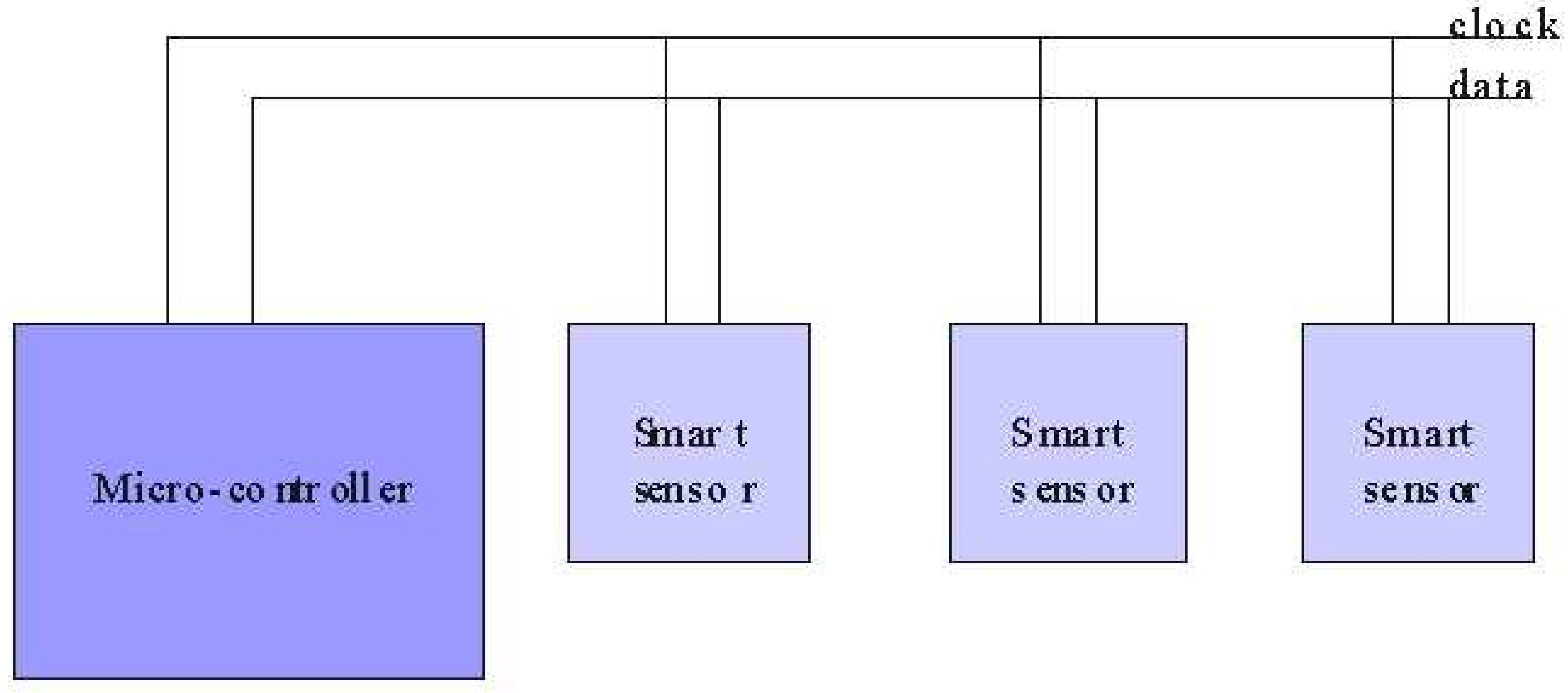
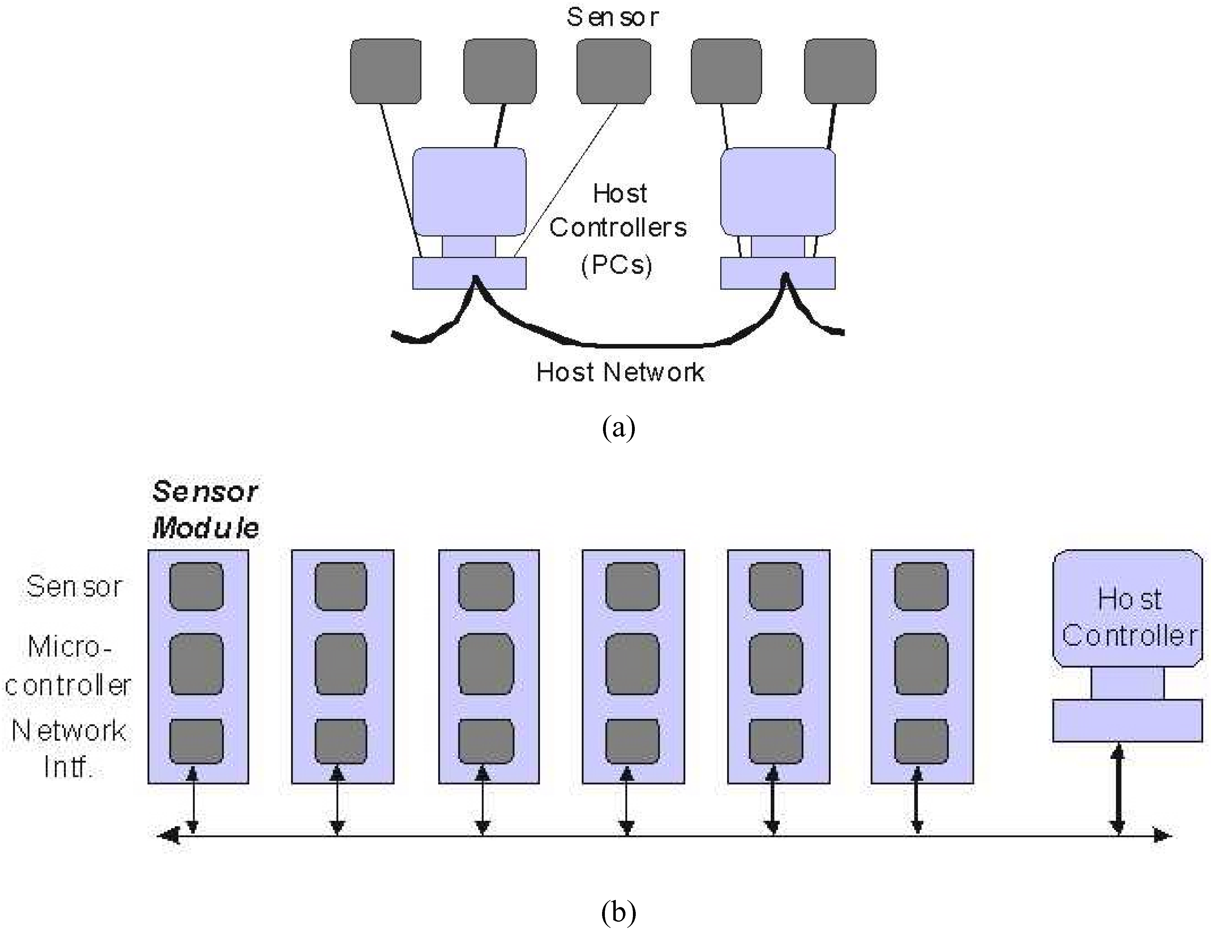
Sensors are increasingly being added to electronic systems to improve performance, increase lifetime, or reduce cost. When multiple sensors are utilized, the system designer must consider how to connect the sensors. When a limited number of sensors are needed, a common architecture is to use point-to-point wiring to connect the sensors to the main control system where the data will be collected. The main controller could be a PC or other control module within a system. This architecture, which is shown in
Figure 5a, requires a minimum design effort where sensors can be integrated into a system with little hardware overhead, primarily using software. Although the main controllers could be networked to share information, this architecture is best for applications where sensor networking is not a primary demand. Due to the point-to-point architecture, sensor modules in this approach can be unsophisticated, “dumb” devices with no required signal processing or networking within the sensor itself.
An alternative architecture which has become quite popular in many applications it to employ “smart sensors” which can be connected on a network (typically hardwired) to a master (host) control system, as shown in
Figure 5b. In this approach, each sensor module contains a sensor, signal processing hardware (typically a microcontroller), and a network interface which may or may not be physically integrated with the microcontroller. The advantage of this architecture is that significant signal processing can take place within the sensor module and, by using a standard network bus, sensors can share information. The I
2C bus is well suited for this architecture, and the TII (IEEE P1451.2) bus can be used when only one sensor module will be connected to the host system. This structure also lends itself well to wireless network applications. A primary disadvantage of this architecture is its limited optimization of resources; typically each sensor module operates as an autonomous unit with no sharing of signal processing and interface hardware even if sensors are located physically together. As a result, it is difficult to optimize the power dissipation or minimize the size of the overall sensor network.
Figure 5.
Sensor networking architectures a) point-to-point connections and b) networked single-sensor modules.
Figure 5.
Sensor networking architectures a) point-to-point connections and b) networked single-sensor modules.
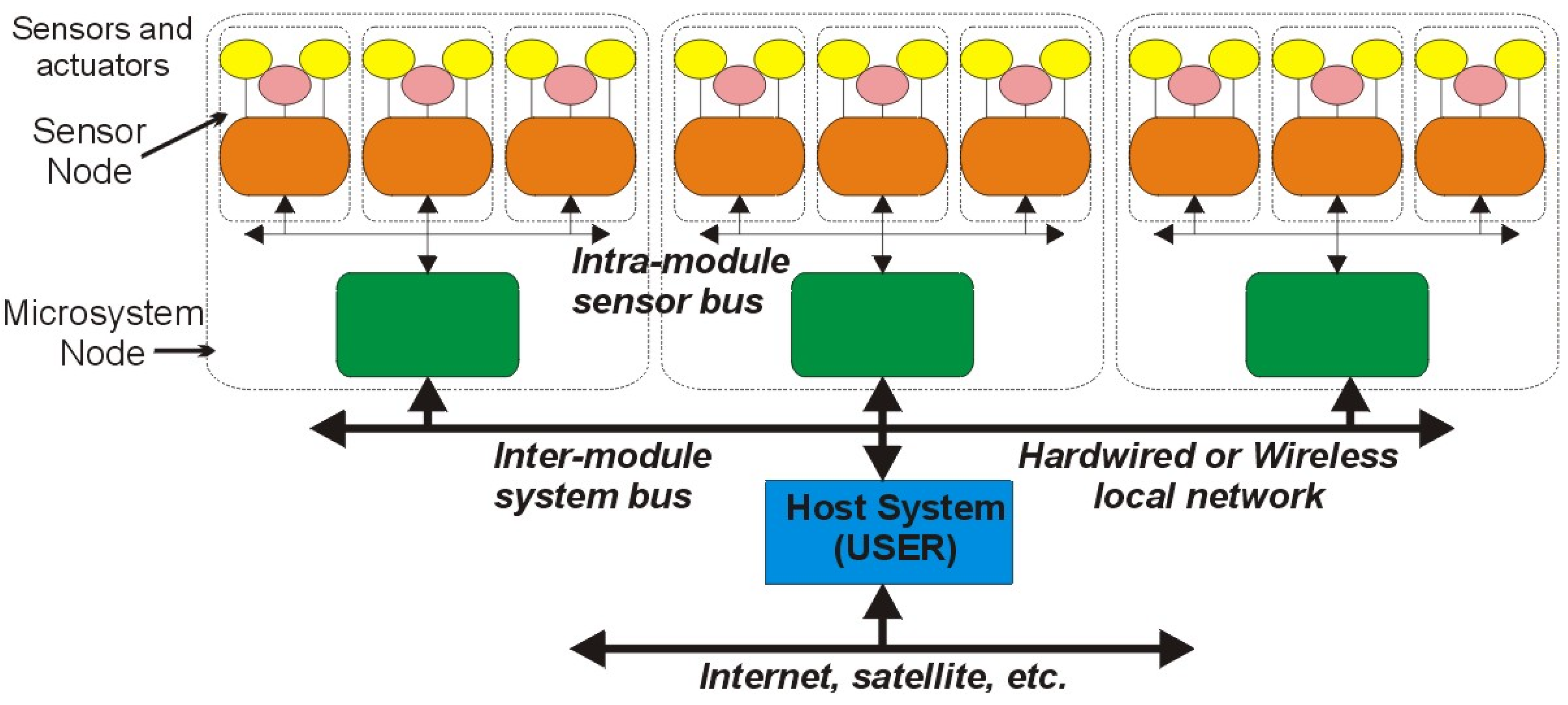
The final sensor system architecture that will be presented involves a much more complex, multilayered network as shown in
Figure 6. This approach utilizes a series of communication busses to transport sensor/actuator data through a sequence of increasingly sophisticated electronics. Here, sensors and actuators are connected directly to signal conditioning circuitry within a sensor node. Individual sensor nodes communicate with a microsystem controller, typically via a hardwired “intramodule” bus, which can perform some signal processing and correlation/fusion of data from the sensor nodes. The microsystem nodes communicate via a system bus, which may be hardwired or wireless depending on application, to share data or report to a host system for further processing and/or long-term storage. Finally, the host system may be connected to a large-scale network, such as the internet. In this architecture, the microsystem node is typically packaged as one physical (often battery powered) module, thus the term “intramodule” bus for the link within the microsystem module. To optimize performance incorporating the unique nature of the intramodule bus, a new sensor bus has been developed and is the subject of the next section of this paper.
Figure 6.
A multi-layered sensor network which utilizes a hardwired “intramodule” sensor bus.
Figure 6.
A multi-layered sensor network which utilizes a hardwired “intramodule” sensor bus.
Figure 7.
A two-layered bus sensor network architecture showing ideal locations of signal conditioning/processing and networking hardware.
Figure 7.
A two-layered bus sensor network architecture showing ideal locations of signal conditioning/processing and networking hardware.
There are several advantages to this architecture in application which utilize a large number of sensors. First, the multi-layered branching network allows a tremendous number of sensors/actuators (typically thousands depending on the specific bus protocols chosen) to be accessed within the same network. Second, this approach optimizes signal processing resources by allowing many functions to be shared thus minimizing redundant electronics.
Figure 7 shows a typical two-layered bus network using this architecture and illustrates ideal locations for signal conditioning, signal processing, and networking hardware which minimizes the required electronics in the overall system. Third, a significant advantage of this approach is a system-wide reduction in power consumption [
9]. Because the resources can be shared and optimized within each microsystem node, each node can operate with minimum power demands, and the layering of signal processing hardware allows the network to intelligently manage resources to reduce redundant operations. Finally, this architecture is very flexible and can be adapted to many sensor network applications.
New Intramodule Sensor Bus for Low Power Microsystems
The Intramodule Multielement Microsystem (IM
2) sensor bus defines a set of specifications to provide a universal interface between a microcontroller and “simple” sensor nodes within a microsystem. As noted above, this intramodule bus fits within the architecture illustrated in
Figure 7. In order to minimize power consumption, physical size, and cost, the “simple” sensor nodes will include signal conditioning and sensor bus communication hardware, but they are not required to implement the complexity of a microcontroller as required by many bus structures. Removing the necessity to have a microcontroller at each sensor node is a key element motivating the development of the IM
2 bus which provides an optimized interface for intramodule communication over a short physical distance.
Figure 8.
Typical IM2 bus configuration.
Figure 8.
Typical IM2 bus configuration.
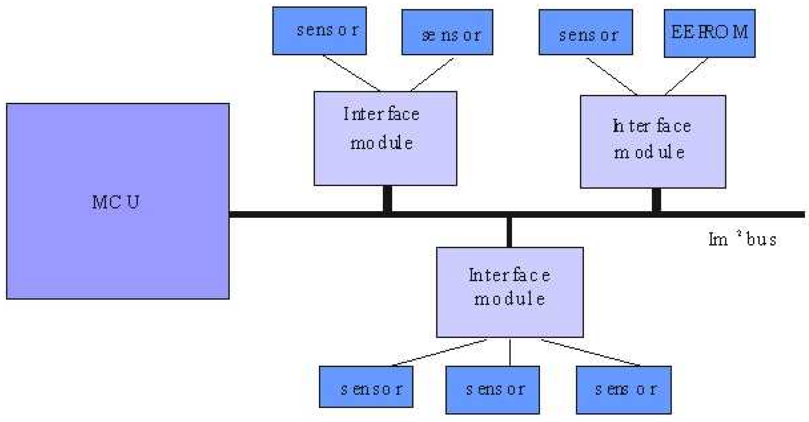
The IM
2 Bus is an expansion of IEEE P1451.2 TII sensor bus and is designed to have one bus controller (NCAP) and many STIMs to support distributed multidrop sensor module nodes as shown in
Figure 8. This bus is also required to support sensor data in both analog and digital formats and offer power management features such as support of normally-off operation. IM
2 bus supports “sleep mode” operation and allows the sensor bus clock to be disabled resulting in a reduction of unutilized power dissipation. Finally, IM
2 bus is designed to be a superset, or extension, of the TII bus which maintains hardware compatibility with TII.
A description of the IM
2 bus signals is given in
Table 1. Although hardware compatibility with the IEEE P1451.2 standard has been maintained (i.e., all of the same signals are used with the same logic and function), the data protocol has been modified, features have been added to support plug-n-play, and an additional (optional) signal has been added. To satisfy the needs of microsystems with multiple internal sensor nodes, the data protocol has been modified since IEEE P1451.2 protocol assumes a point-to-point connection. The primary modifications from the TII bus include:
addition of a chip address byte at the beginning of each instruction
implementation of two addressing modes
- ➢
compact address mode (chip address and function in one 8-bit word)
- ➢
full address mode (chip address and function in individual words)
modification of the NSDET signal function to serve as a plug-n-play indicator
definition of DOUT as either digital, analog, or frequency-coded data
addition of the second power line to support power management features
Table 1.
IM2 bus signals.
Table 1.
IM2 bus signals.
| Line | Description |
|---|
| DIN | Address and data transmitted from microcontroller to interface module |
| DOUT | Data transmitted from interface module to microcontroller |
| DCLK | Positive-going edge latches data on DIN and DOUT |
| NIOE | Signals that data transport is active and delimits data framing |
| NTRIG | Performs triggering function |
| NACK | trigger acknowledge and data transport acknowledge |
| NINT | Used by interface module to request service from microcontroller |
| NSDET | Used by microcontroller to detect the presence of new interface module |
| POWER | Normal 3-V power supply |
| VSWITCH | Controllable power supply. It will be at low when system in sleep mode. |
IM2 maintains both of the advantages of TII and I2C bus. It allows up to 255 smart nodes within each microsystem module of the overall system. Each smart node can be connected to the bus without affecting any circuits on the bus. It supports the plug-n-play function; the microcontroller can easily detect the new node added to the bus. Because some dedicated lines are used for the control signals, the hardware of IM2 is simple and power efficient. IM2 provides a simple but universal interface between the microcontroller and sensors, and is hardware compatible with IEEE1421.2 standard. It is best suited for the microsystems having severe power limitation and short wiring distances between the module controller and the sensor nodes. A full description of this bus structure as well as a sensor interface circuit which implements its protocols will be published in the literature soon.
To aid system designers in choosing the most appropriate sensor bus for a given application, a table comparing bus features is provided in
Table 2. Here, the significant features of each bus discussed in this paper are quantified, relative to each other, as Good, Fair, or Poor.
Table 2.
Summary and comparison of sensor bus features.
Table 2.
Summary and comparison of sensor bus features.
| | Power | Data Bandwidth | System Complexity | Easy for configuration | Plug&Play |
|---|
| I2C | Good | Fair | Good | Good | Poor |
| SPI | Good | Fair | Poor | Poor | Poor |
| IEEE1451.2 TII | Good | Fair | Poor | Fair | Good |
| IEEE1451.3 | Poor | Good | Good | Good | Good |
| IM2 | Good | Fair | Fair | Fair | Good |
Wireless Sensor Networks
Wireless sensor networks combine microsensor technology, low-power signal processing, computation, and low-cost wireless networking in a small system [
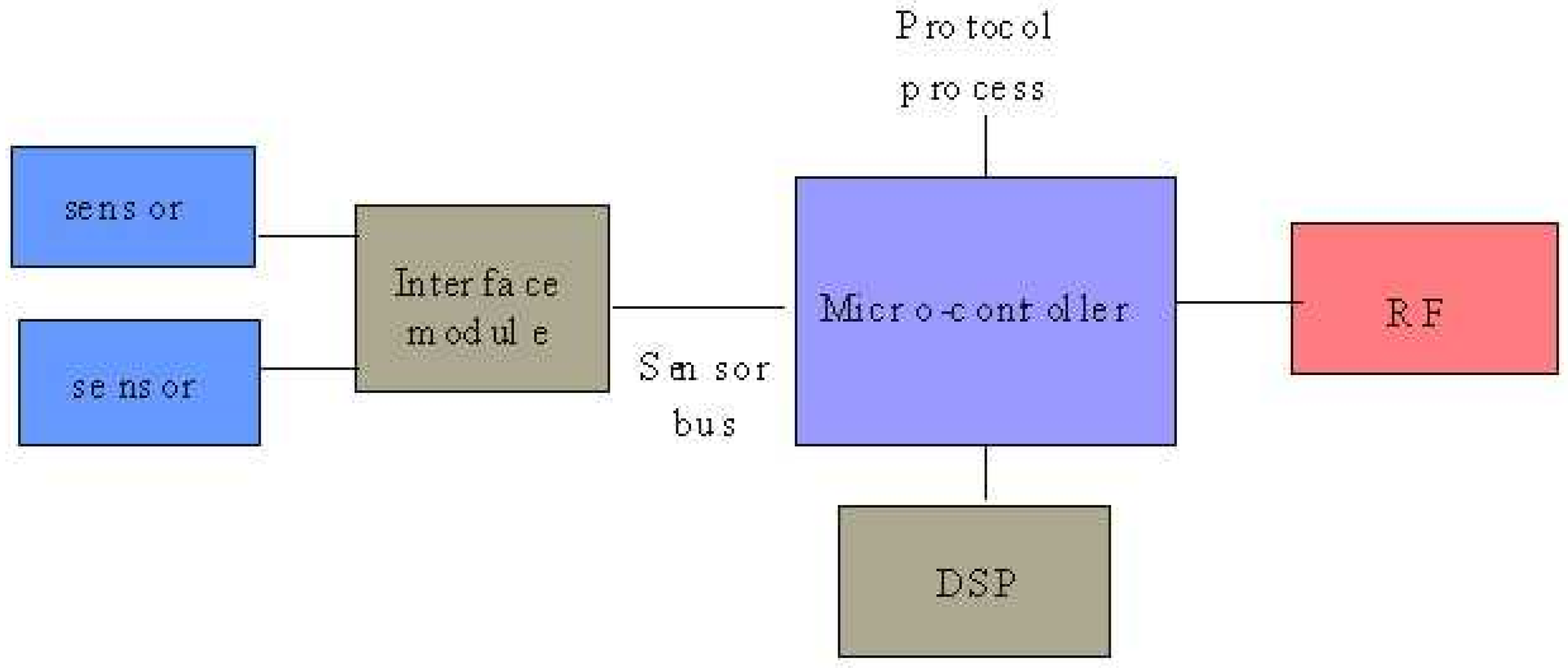
10]. It provides distributed network and internet access to sensors and controls sensors deeply embedded in the environment or facility. Sensor nodes are dispersed over the area of interest and possess the capability of RF communication, signal process, and communication protocols process. It allows hundreds to thousands of nodes to cooperate in the network to achieve a larger task. An example of the sensor node structure for wireless networks is shown in
Figure 9, although as noted above the architecture shown in
Figure 6 and
Figure 7 also supports the wireless networking of microsystem modules.
Figure 9.
Sensor node structure for wireless networks.
Figure 9.
Sensor node structure for wireless networks.
A wireless sensor network is different from the conventional wireless network. The small size of the sensor node limits battery capacity requiring every operation to be done efficiently. It also limits the radio transition range and suggests a small multi-hop transmission structure. Using several short range intermediate nodes to send a bit is much more energy-efficient than using one-long hop. In the multi-hop network, nodes cannot know a priori the optimal route to other nodes. Therefore, a new networking protocol is needed to coordinates the discovery and tracking of routes in the network with minimal power consumption. Also, in the wireless sensor network, the sensor nodes would remain largely inactive for long period of time, and becoming suddenly active when something is detected or the timed event occurs. It motivates a medium-access control (MAC) protocol where energy conservation and self-configuration are of primary importance. In this section, an example of a MAC protocol and a routing protocol, which would be particularly useful for sensor networks, are presented.
Sensor-MAC(S-MAC)
S-MAC [
11] trades energy efficiency for per-hop fairness and latency. It consists of three major components, periodic listen and sleep, collision and overhearing avoidance and message passing. In many sensor network applications, nodes are idle for a long time if no sensing event occurs. S-MAC reduces the listen time by letting nodes go into periodic sleep mode. Before each node starts its periodic listen and sleep, it needs to choose a schedule and exchange that with its neighbors. Each node maintains a schedule table that stores the schedules of all its known neighbors. To prevent longterm clock drift, a maintaining synchronization is specified in S-MAC. Each node periodically updates their schedules and keeps synchronized among neighboring nodes. For collision avoidance, S-MAC follows similar procedures as the 802.11 standard. It uses both virtual and physical carrier sense and RTS/CTS exchange to address the hidden terminal problem. In addition, S-MAC tries to avoid the overhearing problem by letting interfering nodes go to sleep after they hear an RTS or CTS packet. This prevents neighboring nodes from overhearing long packets and consequently saves the receiver energy significantly. In S-MAC, the long messages are broken into many small fragments and are transmitted in burst to reduce the cost of bit corruption in the wireless transmission. To avoid the large control overhead of sending many small packets, the medium are reserved for transmitting all the fragments. Result shows S-MAC can save energy by factor of 2 compared to the 802.11 MAC [
11].
Low Energy Adaptive Clustering Hierarchy (LEACH)
LEACH [
12,
13] assumes the sensor network has a fixed base station to which the sensor data is routed. All the sensor nodes are static, homogeneous and energy constrained. The sensor nodes sense the environment continuously and have their data sent at a fixed rate. LEACH is a cluster based routing algorithm. Cluster heads collect data from all the sensor nodes in their cluster, aggregate the collected data by data fusion methods and transmit the data directly to the base station. It allows the data from nodes within the cluster to be processed locally which reduces the data set that needs to be transmitted. The heads of the clusters are self-elected and remain to be the heads for a period called a round. At the beginning of each round, every node determines if it can be a cluster head during the current round. If yes, the node announces its decision to its neighbors. Other nodes which choose not to be cluster heads can join one of the cluster heads by listening to the announcements by the selfselected heads. Randomized rotation of the high-energy cluster head position is incorporated in LEACH to avoid draining the battery of any one node in the network. TDMA is used for media access. The cluster-head creates a TDMA schedule that tells each node exactly when to transmit its data. It allows the nodes to remain in the sleep state as long as possible and avoid intra-cluster collision. This protocol is reported to extend the life of wireless sensor networks by a factor of eight compared to the conventional multi hop routing and static clustering networking protocols.
Conclusion
A serial bus structure provides the minimum number of interconnects in the sensor network and is generally used in a smart sensor system to provide low cost and high reliability. Several existing serial buses, I2C, SPI, IEEE1451.2 TII and IEEE1451.3 have been reviewed to define the advantages and disadvantages of each bus for different applications. A review of sensor network architectures has been presented to illustrate where these busses would be useful depending on the architecture employed. A new sensor bus, IM2, has been briefly introduced as an intramodule bus in a multi-layered sensor network. IM2 maintains the advantages of both the IEEE1451.2 TII and the I2C bus, but IM2 is optimized for low power microsystem applications with short wiring distances between the microsystem module controller and the sensor nodes. Finally, some issues with low power protocols for wireless sensor networks have been discussed and some examples have been presented.


