
Analysis of Effects of Surface Roughness on Sensing Performance of Surface Plasmon Resonance Detection for Refractive Index Sensing Application


Abstract
:1. Introduction
2. Materials and Methods
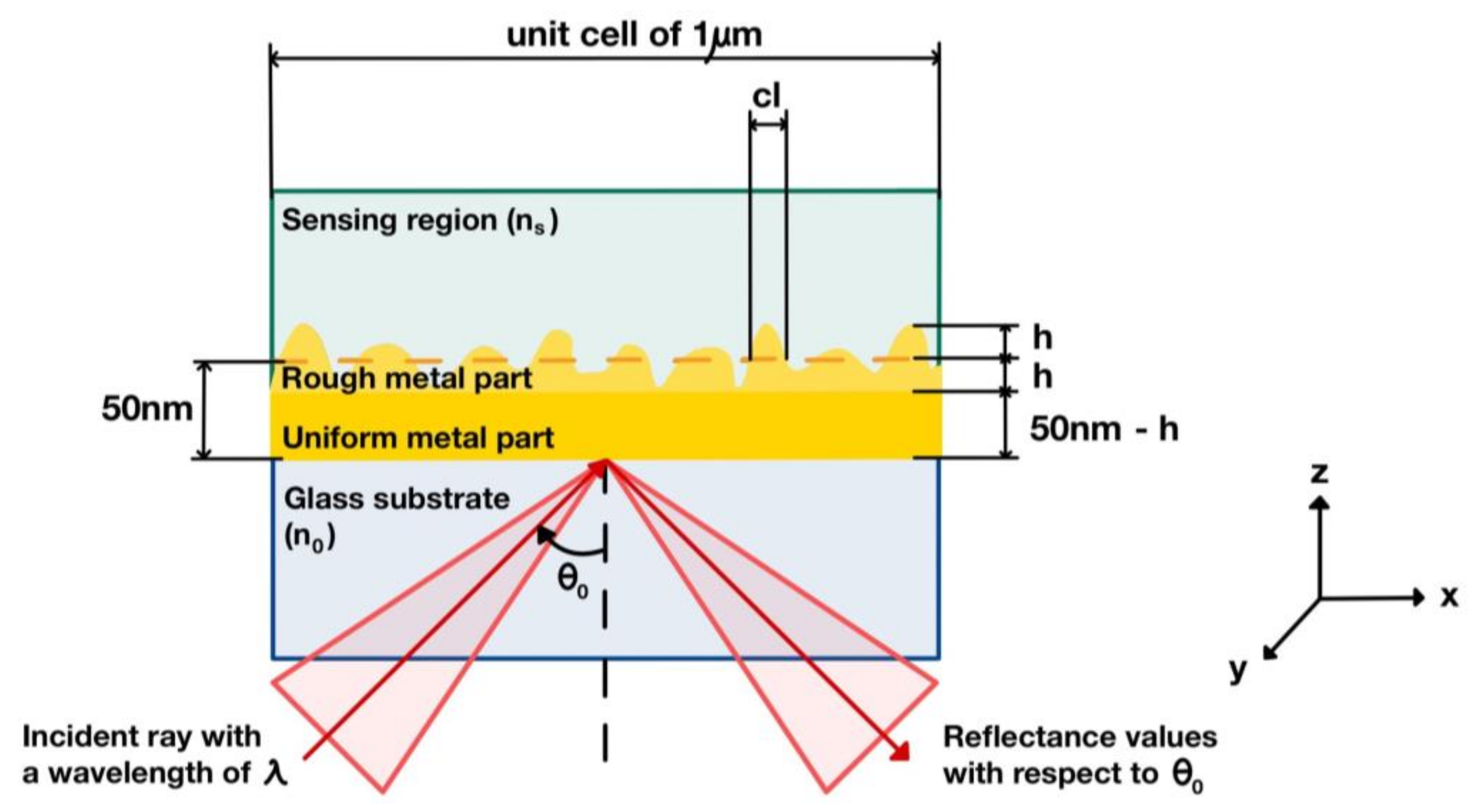
2.1. Surface Plasmon Resonance Detection and Rough Surface Model
- (1)
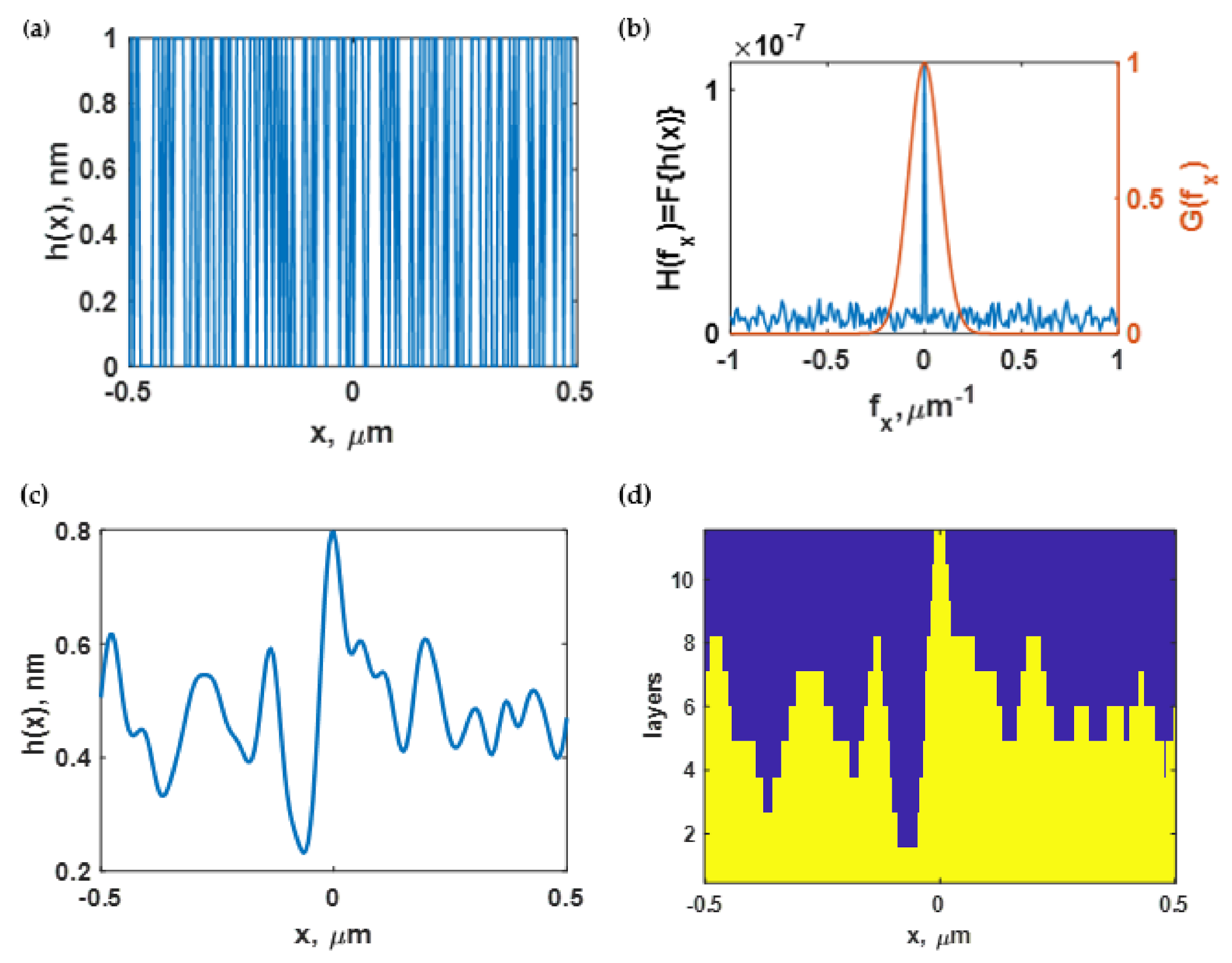
- Generate a random surface profile with digital numbers 0 and 1 and multiply by the expected , where is the spatial distance along the x-axis of the substrate, as depicted in Figure 4a.
- (2)
- Fourier transform the generated surface , where is the Fourier-transformed profile, fx is the Fourier domain axis, and is the Fourier-transform operator, as depicted in Figure 4b.
- (3)
- Low-pass filter the Fourier surface profile using the Gaussian distribution function expressed as shown in Equation (1) and depicted by red curves in Figure 4b.
- (4)
- Inverse Fourier transform the product of to obtain the rough surface profile, as depicted in Figure 4c.
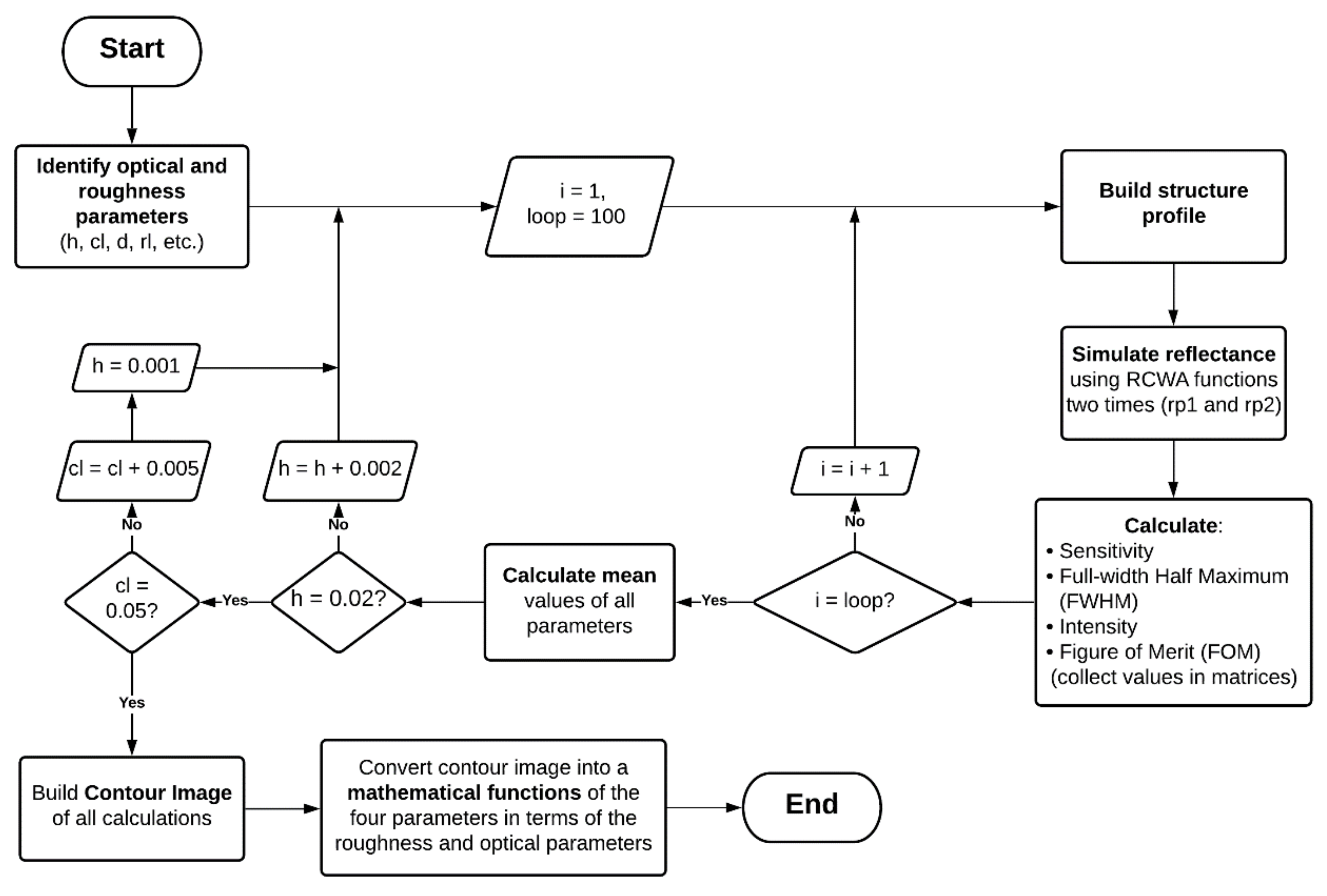
2.2. Optical Simulation Using Rigorous Coupled-Wave Analysis
2.3. Quantitative Performance Parameters
- (1)
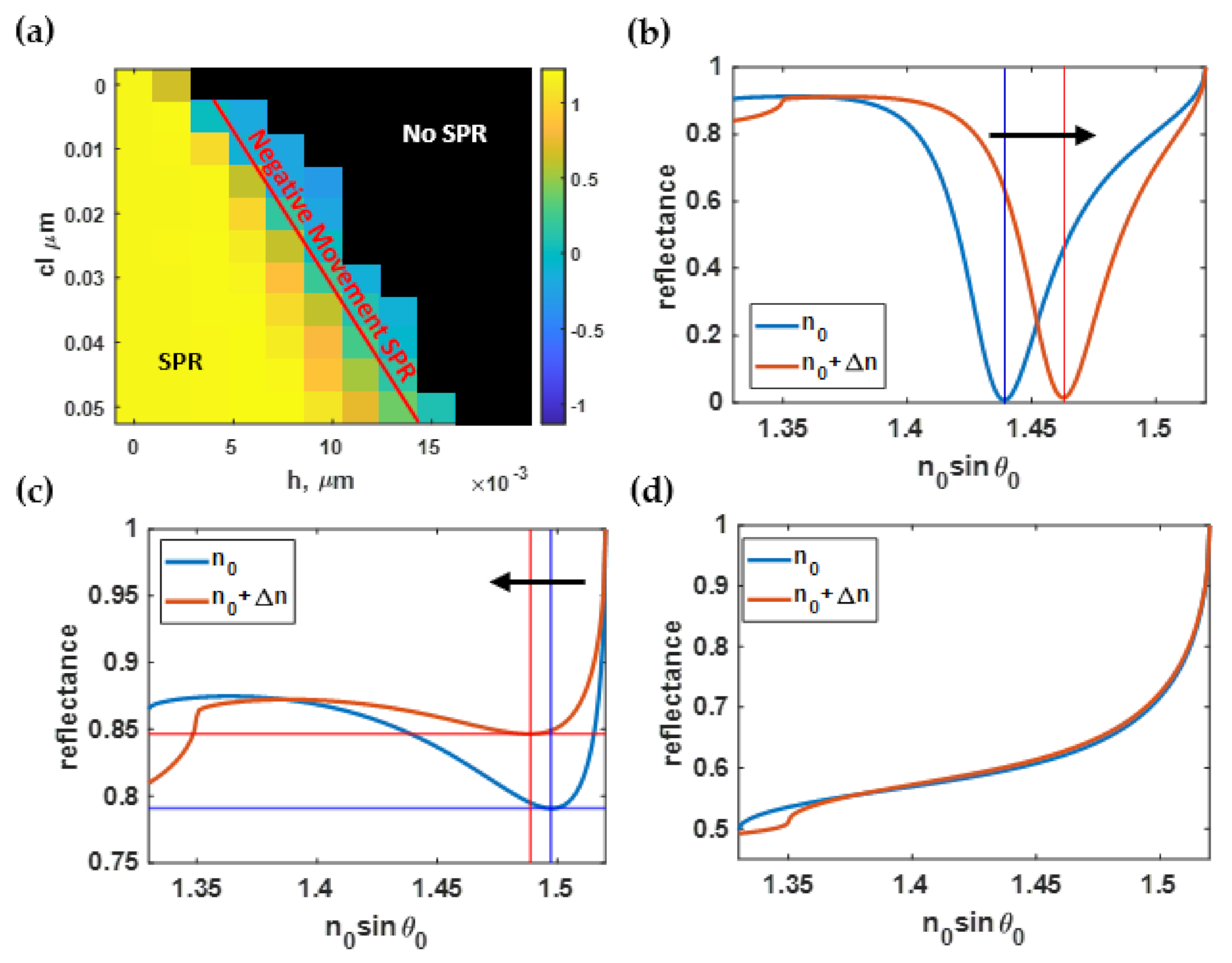
- Sensitivity (S) was defined as the change in plasmonic wave vector (ksp) over the change in refractive index (ns) in the sensing region, as depicted in Figure 6a and expressed in Equation (3). The unit of S is rad RIU−1/μm. Note that RIU stands for refractive index unit.
- (2)
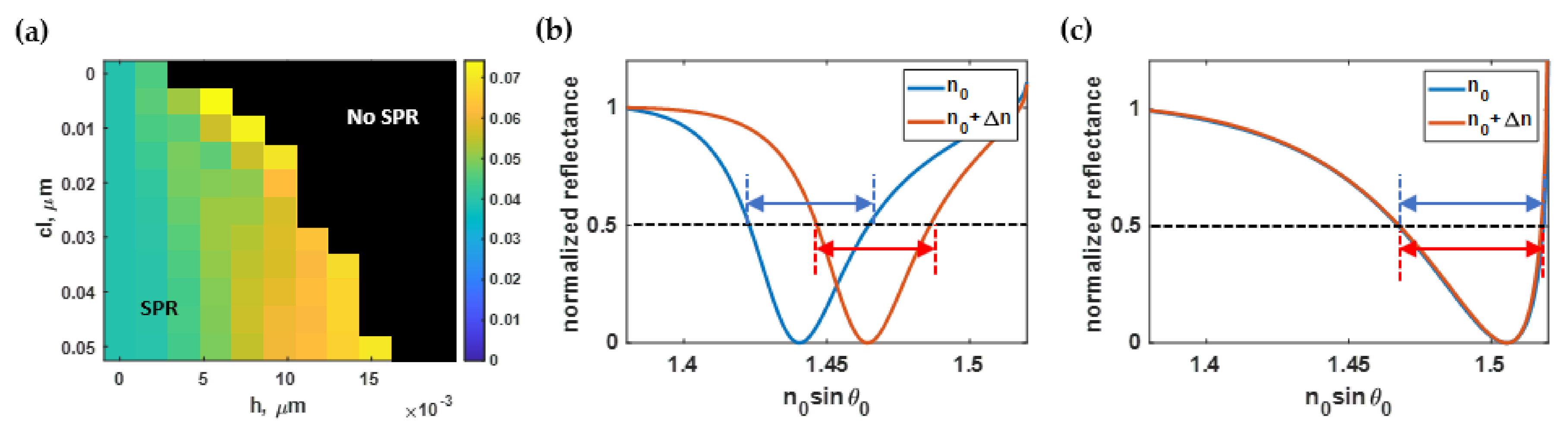
- The full width at half maximum (FWHM) was defined as the average width of the SPR dips with the ns of 1.33 and 1.35 cases in wave-vector space with an optical intensity of at least 0.5 (50%) of the normalized optical reflectance spectra, as depicted in Figure 6b and expressed in Equation (4). Thus, the unit of the FWHM is rad/μm.where and are the FWHM of the normalized SPR reflectance spectra when the refractive index of the sensing region was 1.33 and 1.35, respectively.
- (3)
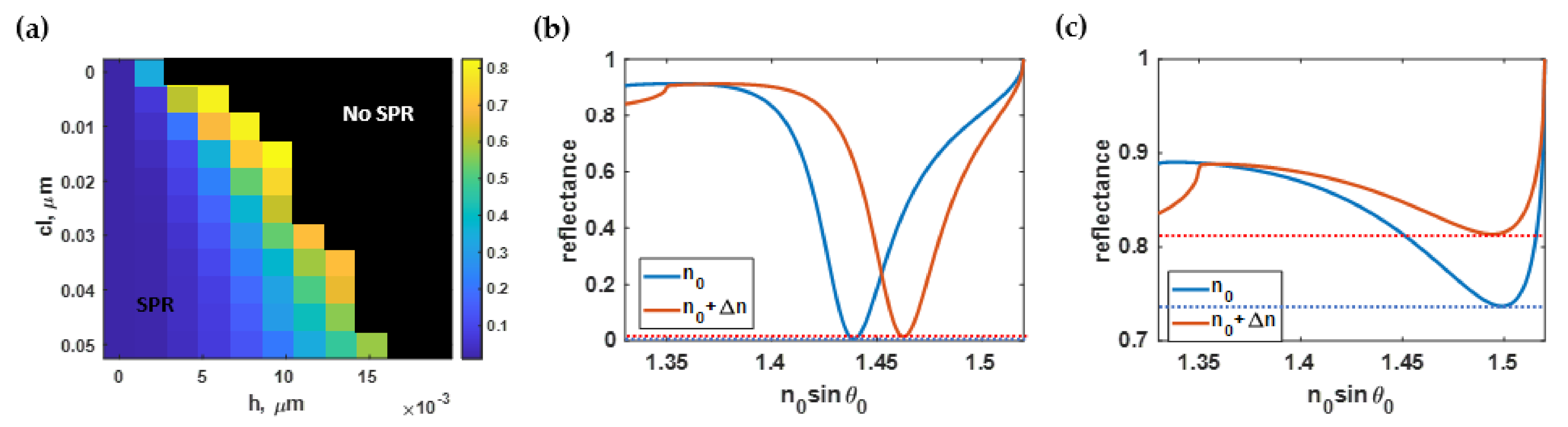
- Intensity contrast () was the average change in optical reflectance at the two plasmonic dips, as shown in Figure 6a and expressed by Equation (5):where and are the change in optical reflectance at the plasmonic angles when the refractive index of the sensing region was 1.33 and 1.35, respectively.
- (4)
- Optical reflectance at the plasmonic angle () was defined as the average optical reflectance ( and ) of the two plasmonic dips when the refractive index of the sensing region was 1.33 and 1.35, as expressed in Equation (6):
- (5)
- The figure of merit (FOM) was defined by considering the dip movement, the FWHM, and the intensity level. Here, the FOM was defined as shown in Equation (7):

3. Results and Discussion
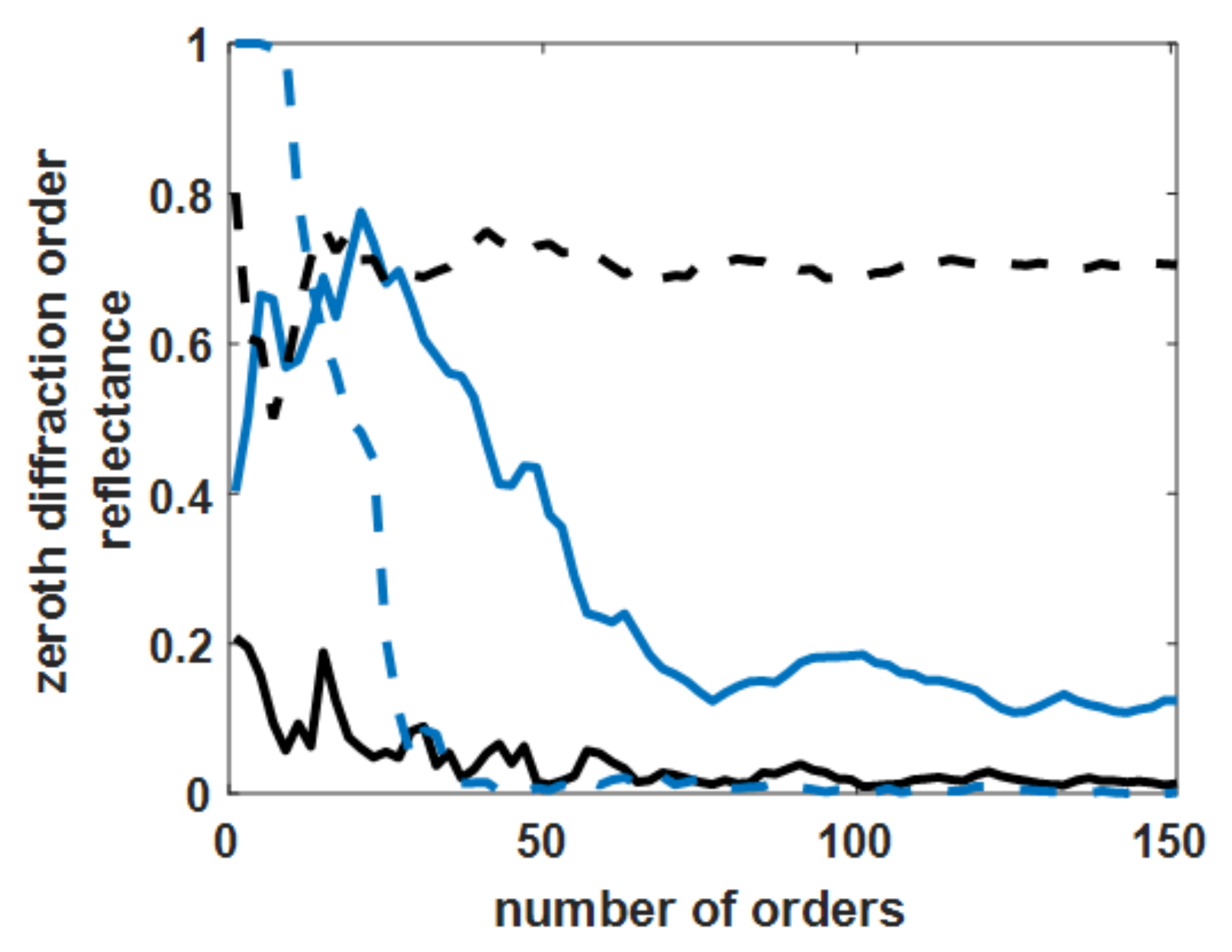
3.1. Convergence Test of Extreme Cases
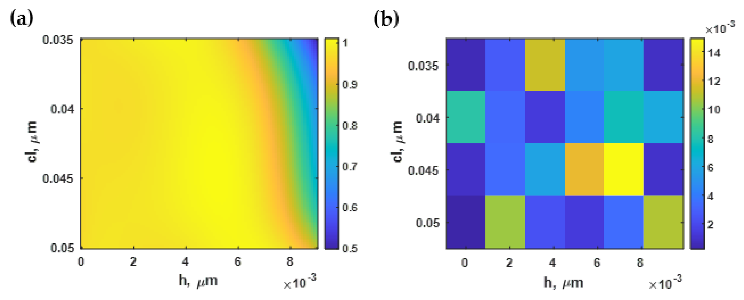
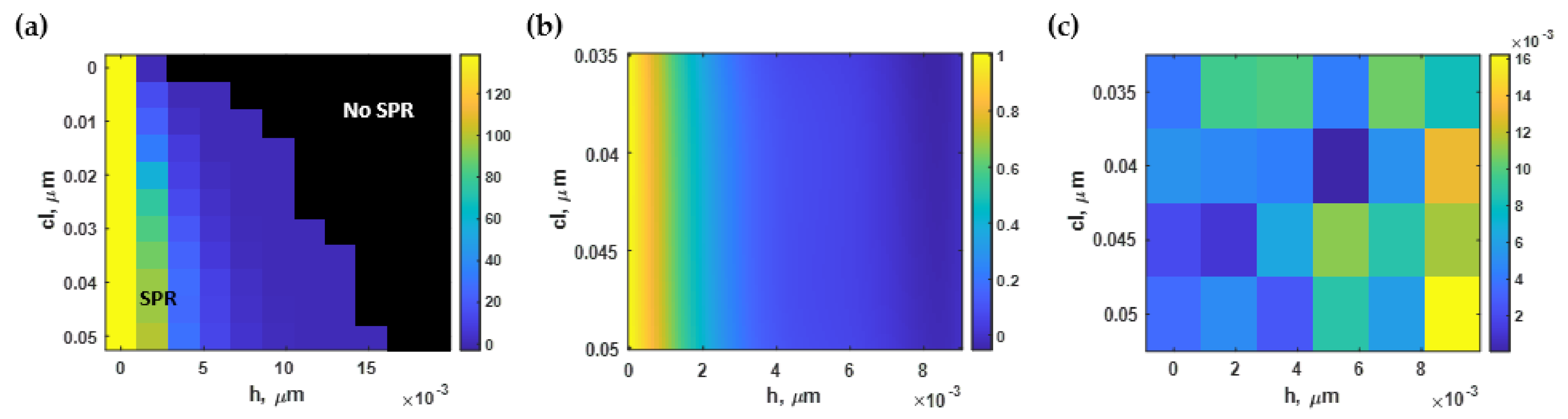
3.2. Effect of Roughness on the SPR Sensitivity
3.3. Effect of Roughness on the SPR Full Width at Half Maximum (FWHM)
3.4. Effect of Roughness on the Intensity Contrast (ΔI)
3.5. Effect of Roughness on the SPR Dip Intensity (Isp)
3.6. Effect of Roughness on the SPR Figure of Merit (FOM)
3.7. Plasmonic Sensing Responses of Different Depositions and Surface-Treatment Technologies
4. Conclusions
Author Contributions
Funding
Institutional Review Board Statement
Informed Consent Statement
Data Availability Statement
Acknowledgments
Conflicts of Interest
References
- Brongersma, M.L.; Kik, P.G. Surface Plasmon Nanophotonics; Springer: Berlin/Heidelberg, Germany, 2007; Volume 131. [Google Scholar]
- Somekh, M.G.; Pechprasarn, S. Surface plasmon, surface wave, and enhanced evanescent wave microscopy. In Handbook of Photonics for Biomedical Engineering; Springer Netherlands: Dordrecht, the Netherlands, 2017; pp. 503–543. [Google Scholar]
- Mariani, S.; Minunni, M. Surface plasmon resonance applications in clinical analysis. Anal. Bioanal. Chem. 2014, 406, 2303–2323. [Google Scholar] [CrossRef]
- Chen, J.; Park, B. Label-free screening of foodborne Salmonella using surface plasmon resonance imaging. Anal. Bioanal. Chem. 2018, 410, 5455–5464. [Google Scholar] [CrossRef]
- Douzi, B. Protein–protein interactions: Surface plasmon resonance. In Bacterial Protein Secretion Systems; Springer: Berlin/Heidelberg, Germany, 2017; pp. 257–275. [Google Scholar]
- Drescher, D.G.; Selvakumar, D.; Drescher, M.J. Analysis of protein interactions by surface plasmon resonance. Adv. Protein Chem. Struct. Biol. 2018, 110, 1–30. [Google Scholar]
- Sangworasil, M.; Pechprasarn, S.; Learkthanakhachon, S.; Ittipornnuson, K.; Suvarnaphaet, P.; Albutt, N. Investigation on feasibility of using surface plasmons resonance (SPR) sensor for ultrasonic detection: A novel optical detection of ultrasonic waves. In Proceedings of the 2016 9th Biomedical Engineering International Conference (BMEiCON), Luang Prabang, Laos, 7–9 December 2016; IEEE: New York, NY, USA, 2016; pp. 1–3. [Google Scholar]
- Shen, M.; Learkthanakhachon, S.; Pechprasarn, S.; Zhang, Y.; Somekh, M.G. Adjustable microscopic measurement of nanogap waveguide and plasmonic structures. Appl. Opt. 2018, 57, 3453–3462. [Google Scholar] [CrossRef]
- Suvarnaphaet, P.; Pechprasarn, S. Enhancement of long-range surface plasmon excitation, dynamic range and figure of merit using a dielectric resonant cavity. Sensors 2018, 18, 2757. [Google Scholar] [CrossRef] [Green Version]
- Suvarnaphaet, P.; Pechprasarn, S. Quantitative Cross-Platform Performance Comparison between Different Detection Mechanisms in Surface Plasmon Sensors for Voltage Sensing. Sensors 2018, 18, 3136. [Google Scholar] [CrossRef] [Green Version]
- Pechprasarn, S.; Chow, T.W.; Somekh, M.G. Application of confocal surface wave microscope to self-calibrated attenuation coefficient measurement by Goos-Hänchen phase shift modulation. Sci. Rep. 2018, 8, 8547. [Google Scholar] [CrossRef] [PubMed]
- Chow, T.W.; Pechprasarn, S.; Meng, J.; Somekh, M.G. Single shot embedded surface plasmon microscopy with vortex illumination. Opt. Express 2016, 24, 10797–10805. [Google Scholar] [CrossRef] [PubMed]
- Lan, J.; Ge, J.; Yu, J.; Shan, S.; Zhou, H.; Fan, S.; Zhang, Q.; Shi, X.; Wang, Q.; Zhang, L. Structure of the SARS-CoV-2 spike receptor-binding domain bound to the ACE2 receptor. Nature 2020, 581, 215–220. [Google Scholar] [CrossRef] [PubMed] [Green Version]
- Otto, A. Excitation of nonradiative surface plasma waves in silver by the method of frustrated total reflection. Z. Phys. A Hadron. Nucl. 1968, 216, 398–410. [Google Scholar] [CrossRef]
- Kretschmann, E.; Raether, H. Radiative decay of non radiative surface plasmons excited by light. Z. Nat. A 1968, 23, 2135–2136. [Google Scholar] [CrossRef]
- Barthes, J.; Bouhelier, A.; Dereux, A.; Des Francs, G.C. Coupling of a dipolar emitter into one-dimensional surface plasmon. Sci. Rep. 2013, 3, 2734. [Google Scholar] [CrossRef] [PubMed]
- De Leon, N.P.; Shields, B.J.; Chun, L.Y.; Englund, D.E.; Akimov, A.V.; Lukin, M.D.; Park, H. Tailoring light-matter interaction with a nanoscale plasmon resonator. Phys. Rev. Lett. 2012, 108, 226803. [Google Scholar] [CrossRef] [Green Version]
- Schasfoort, R.B. Handbook of Surface Plasmon Resonance; Royal Society of Chemistry: Cambridge, UK, 2017. [Google Scholar]
- Homola, J. Present and future of surface plasmon resonance biosensors. Anal. Bioanal. Chem. 2003, 377, 528–539. [Google Scholar] [CrossRef] [PubMed]
- Gaylord, T.K.; Moharam, M. Analysis and applications of optical diffraction by gratings. Proc. IEEE 1985, 73, 894–937. [Google Scholar] [CrossRef]
- Moharam, M.; Gaylord, T. Rigorous coupled-wave analysis of planar-grating diffraction. JOSA 1981, 71, 811–818. [Google Scholar] [CrossRef]
- Barer, R.; Tkaczyk, S. Refractive index of concentrated protein solutions. Nature 1954, 173, 821–822. [Google Scholar] [CrossRef]
- Pechprasarn, S.; Learkthanakhachon, S.; Zheng, G.; Shen, H.; Lei, D.Y.; Somekh, M.G. Grating-coupled Otto configuration for hybridized surface phonon polariton excitation for local refractive index sensitivity enhancement. Opt. Express 2016, 24, 19517–19530. [Google Scholar] [CrossRef]
- Ashley, J.; D’Aurelio, R.; Piekarska, M.; Temblay, J.; Pleasants, M.; Trinh, L.; Rodgers, T.L.; Tothill, I.E. Development of a β-Lactoglobulin sensor based on SPR for milk allergens detection. Biosensors 2018, 8, 32. [Google Scholar] [CrossRef] [Green Version]
- Miller, M.S.; Ferrato, M.-A.; Niec, A.; Biesinger, M.C.; Carmichael, T.B. Ultrasmooth gold surfaces prepared by chemical mechanical polishing for applications in nanoscience. Langmuir 2014, 30, 14171–14178. [Google Scholar] [CrossRef]
- Leandro, L.; Malureanu, R.; Rozlosnik, N.; Lavrinenko, A. Ultrathin, ultrasmooth gold layer on dielectrics without the use of additional metallic adhesion layers. ACS Appl. Mater. Interfaces 2015, 7, 5797–5802. [Google Scholar] [CrossRef] [PubMed] [Green Version]
- Diebel, J.; Löwe, H.; Samori, P.; Rabe, J. Fabrication of large-scale ultra-smooth metal surfaces by a replica technique. Appl. Phys. A 2001, 73, 273–279. [Google Scholar] [CrossRef]
- Nagpal, P.; Lindquist, N.C.; Oh, S.-H.; Norris, D.J. Ultrasmooth patterned metals for plasmonics and metamaterials. Science 2009, 325, 594–597. [Google Scholar] [CrossRef]
- Hegner, M.; Wagner, P.; Semenza, G. Ultralarge atomically flat template-stripped Au surfaces for scanning probe microscopy. Surf. Sci. 1993, 291, 39–46. [Google Scholar] [CrossRef]
- Gutés, A.; Carraro, C.; Maboudian, R. Ultrasmooth gold thin films by self-limiting galvanic displacement on silicon. ACS Appl. Mater. Interfaces 2011, 3, 1581–1584. [Google Scholar] [CrossRef] [PubMed]
- Wieduwilt, T.; Kirsch, K.; Dellith, J.; Willsch, R.; Bartelt, H. Optical Fiber Micro-Taper with Circular Symmetric Gold Coating for Sensor Applications Based on Surface Plasmon Resonance. Plasmonics 2013, 8, 545–554. [Google Scholar] [CrossRef]
- Ng, D.K.; Bhola, B.S.; Bakker, R.M.; Ho, S.T. Ultrasmooth gold films via pulsed laser deposition. Adv. Funct. Mater. 2011, 21, 2587–2592. [Google Scholar] [CrossRef]
- Zhang, C.; Li, J.; Belianinov, A.; Ma, Z.; Renshaw, C.K.; Gelfand, R.M. Nanoaperture fabrication in ultra-smooth single-grain gold films with helium ion beam lithography. Nanotechnology 2020, 31, 465302. [Google Scholar] [CrossRef] [PubMed]
- Zhang, J.; Irannejad, M.; Yavuz, M.; Cui, B. Gold nanohole array with sub-1 nm roughness by annealing for sensitivity enhancement of extraordinary optical transmission biosensor. Nanoscale Res. Lett. 2015, 10, 1–8. [Google Scholar] [CrossRef] [Green Version]
- Pechprasarn, S.; Somekh, M.G. Detection limits of confocal surface plasmon microscopy. Biomed. Opt. Express 2014, 5, 1744–1756. [Google Scholar] [CrossRef] [Green Version]
- Shankaran, D.R.; Gobi, K.V.; Miura, N. Recent advancements in surface plasmon resonance immunosensors for detection of small molecules of biomedical, food and environmental interest. Sens. Actuators B Chem. 2007, 121, 158–177. [Google Scholar] [CrossRef]
- Braundmeier Jr, A.; Arakawa, E. Effect of surface roughness on surface plasmon resonance absorption. J. Phys. Chem. Solids 1974, 35, 517–520. [Google Scholar] [CrossRef]
- Hoffmann, A.; Lenkefi, Z.; Szentirmay, Z. Effect of roughness on surface plasmon scattering in gold films. J. Phys. Condens. Matter 1998, 10, 5503. [Google Scholar] [CrossRef]
- Rahman, T.S.; Maradudin, A.A. Surface-plasmon dispersion relation in the presence of surface roughness. Phys. Rev. B 1980, 21, 2137. [Google Scholar] [CrossRef]
- Crowell, J.; Ritchie, R. Surface-plasmon effect in the reflectance of a metal. JOSA 1970, 60, 794–799. [Google Scholar] [CrossRef]
- Huang, J.-S.; Callegari, V.; Geisler, P.; Brüning, C.; Kern, J.; Prangsma, J.C.; Wu, X.; Feichtner, T.; Ziegler, J.; Weinmann, P. Atomically flat single-crystalline gold nanostructures for plasmonic nanocircuitry. Nat. Commun. 2010, 1, 1–8. [Google Scholar] [CrossRef]
- Chiu, N.-F.; Kuo, C.-T.; Lin, T.-L.; Chang, C.-C.; Chen, C.-Y. Ultra-high sensitivity of the non-immunological affinity of graphene oxide-peptide-based surface plasmon resonance biosensors to detect human chorionic gonadotropin. Biosens. Bioelectron. 2017, 94, 351–357. [Google Scholar] [CrossRef]
- Kurihara, K.; Suzuki, K. Theoretical understanding of an absorption-based surface plasmon resonance sensor based on Kretchmann’s theory. Anal. Chem. 2002, 74, 696–701. [Google Scholar] [CrossRef]
- Otto, A. Investigation of electrode surfaces by surface plasmon polariton spectroscopy. Surf. Sci. 1980, 101, 99–108. [Google Scholar] [CrossRef]
- Nishida, M.; Matsumoto, T.; Koga, H.; Kosako, T.; Kadoya, Y. Evaluation of surface roughness of metal films using plasmonic Fano resonance in attenuated total reflection. Phys. Rev. B 2020, 101, 085414. [Google Scholar] [CrossRef] [Green Version]
- Parmigiani, F.; Scagliotti, M.; Samoggia, G.; Ferraris, G. Influence of the growth conditions on the optical properties of thin gold films. Thin Solid Film. 1985, 125, 229–234. [Google Scholar] [CrossRef]
- Raether, H. The dispersion relation of surface plasmons on rough surfaces; a comment on roughness data. Surf. Sci. 1983, 125, 624–634. [Google Scholar] [CrossRef]
- Kolomenski, A.; Kolomenskii, A.; Noel, J.; Peng, S.; Schuessler, H. Propagation length of surface plasmons in a metal film with roughness. Appl. Opt. 2009, 48, 5683–5691. [Google Scholar] [CrossRef]
- Yang, Z.; Liu, C.; Gao, Y.; Wang, J.; Yang, W. Influence of surface roughness on surface plasmon resonance phenomenon of gold film. Chin. Opt. Lett. 2016, 14, 042401. [Google Scholar]
- Hasan, M.R.; Akter, S.; Rahman, M.S.; Ahmed, K. Design of a surface plasmon resonance refractive index sensor with high sensitivity. Opt. Eng. 2017, 56, 087101. [Google Scholar] [CrossRef]
- Agarwal, S.; Giri, P.; Prajapati, Y.K.; Chakrabarti, P. Effect of surface roughness on the performance of optical SPR sensor for sucrose detection: Fabrication, characterization, and simulation study. IEEE Sens. J. 2016, 16, 8865–8873. [Google Scholar] [CrossRef]
- Byun, K.M.; Yoon, S.J.; Kim, D. Effect of surface roughness on the extinction-based localized surface plasmon resonance biosensors. Appl. Opt. 2008, 47, 5886–5892. [Google Scholar] [CrossRef] [PubMed]
- Tran, N.H.T.; Phan, B.T.; Yoon, W.J.; Khym, S.; Ju, H. Dielectric metal-based multilayers for surface plasmon resonance with enhanced quality factor of the plasmonic waves. J. Electron. Mater. 2017, 46, 3654–3659. [Google Scholar] [CrossRef]
- Diao, W.; Tang, M.; Ding, S.; Li, X.; Cheng, W.; Mo, F.; Yan, X.; Ma, H.; Yan, Y. Highly sensitive surface plasmon resonance biosensor for the detection of HIV-related DNA based on dynamic and structural DNA nanodevices. Biosens. Bioelectron. 2018, 100, 228–234. [Google Scholar] [CrossRef]
- Fabini, E.; Danielson, U.H. Monitoring drug–serum protein interactions for early ADME prediction through Surface Plasmon Resonance technology. J. Pharm. Biomed. Anal. 2017, 144, 188–194. [Google Scholar] [CrossRef]
- Cao, Y.; Griffith, B.; Bhomkar, P.; Wishart, D.S.; McDermott, M.T. Functionalized gold nanoparticle-enhanced competitive assay for sensitive small-molecule metabolite detection using surface plasmon resonance. Analyst 2018, 143, 289–296. [Google Scholar] [CrossRef] [PubMed]
- Miyazaki, C.M.; Shimizu, F.M.; Mejía-Salazar, J.; Oliveira, O.N., Jr.; Ferreira, M. Surface plasmon resonance biosensor for enzymatic detection of small analytes. Nanotechnology 2017, 28, 145501. [Google Scholar] [CrossRef]
- Taylor, A.B.; Zijlstra, P. Single-molecule plasmon sensing: Current status and future prospects. ACS Sens. 2017, 2, 1103–1122. [Google Scholar] [CrossRef] [Green Version]
- Kabashin, A.V.; Evans, P.; Pastkovsky, S.; Hendren, W.; Wurtz, G.A.; Atkinson, R.; Pollard, R.; Podolskiy, V.; Zayats, A.V. Plasmonic nanorod metamaterials for biosensing. Nat. Mater. 2009, 8, 867–871. [Google Scholar] [CrossRef]
- Thadson, K.; Visitsattapongse, S.; Pechprasarn, S. Deep learning-based single-shot phase retrieval algorithm for surface plasmon resonance microscope based refractive index sensing application. Sci. Rep. 2021, 11, 16289. [Google Scholar]
- Berini, P. Long-range surface plasmon polaritons. Adv. Opt. Photonics 2009, 1, 484–588. [Google Scholar] [CrossRef]
- Sreekanth, K.V.; Alapan, Y.; ElKabbash, M.; Ilker, E.; Hinczewski, M.; Gurkan, U.A.; De Luca, A.; Strangi, G. Extreme sensitivity biosensing platform based on hyperbolic metamaterials. Nat. Mater. 2016, 15, 621–627. [Google Scholar] [CrossRef] [Green Version]
- Garoli, D.; Calandrini, E.; Giovannini, G.; Hubarevich, A.; Caligiuri, V.; De Angelis, F. Nanoporous gold metamaterials for high sensitivity plasmonic sensing. Nanoscale Horiz. 2019, 4, 1153–1157. [Google Scholar] [CrossRef]
- Johnson, P.B.; Christy, R.-W. Optical constants of the noble metals. Phys. Rev. B 1972, 6, 4370. [Google Scholar] [CrossRef]
- Sexton, B.; Feltis, B.; Davis, T. Characterization of gold surface plasmon resonance sensor substrates. Sens. Actuators A Phys. 2008, 141, 471–475. [Google Scholar] [CrossRef]
- Liu, S.; Ma, Y.; Chen, X.; Zhang, C. Estimation of the convergence order of rigorous coupled-wave analysis for binary gratings in optical critical dimension metrology. Opt. Eng. 2012, 51, 081504. [Google Scholar] [CrossRef] [Green Version]
- Zhang, B.; Pechprasarn, S.; Somekh, M.G. Quantitative plasmonic measurements using embedded phase stepping confocal interferometry. Opt. Express 2013, 21, 11523–11535. [Google Scholar] [CrossRef] [PubMed]
- Fu, D.; Choi, W.; Sung, Y.; Yaqoob, Z.; Dasari, R.R.; Feld, M. Quantitative dispersion microscopy. Biomed. Opt. Express 2010, 1, 347–353. [Google Scholar] [CrossRef] [PubMed]
- Meng, Q.-Q.; Zhao, X.; Lin, C.-Y.; Chen, S.-J.; Ding, Y.-C.; Chen, Z.-Y. Figure of merit enhancement of a surface plasmon resonance sensor using a low-refractive-index porous silica film. Sensors 2017, 17, 1846. [Google Scholar] [CrossRef] [PubMed]
- Li, R.; Wu, D.; Liu, Y.; Yu, L.; Yu, Z.; Ye, H. Infrared plasmonic refractive index sensor with ultra-high figure of merit based on the optimized all-metal grating. Nanoscale Res. Lett. 2017, 12, 1–6. [Google Scholar] [CrossRef] [Green Version]


| Method | Remaining Root Mean Square (RMS) Roughness |
|---|---|
| No treatment: sputter coating | RMS = 1.2 nm |
| Chemical polishing [25,26] | RMS = 0.38 ± 0.05 nm |
| Mica substrate utilizing [27] | RMS = 0.2 nm |
| Chemically grown single-crystalline gold [31] | RMS < 1 nm |
| Laser ablation [32] | RMS = 0.17 nm |
| Helium ion beam [33] | RMS = 0.267 nm |
| Thermal annealing [34] | RMS < 1 nm |
| Method | RMS Roughness (nm) | S (rad · RIU−1/μm) | θsp (Degree) | FWHM (rad/μm) | ΔI | Isp | FOM |
|---|---|---|---|---|---|---|---|
| Ideal smooth surface | 0 | 7.46 | 71.40 | 0.039 | 0.64 | 0.007 | 139.16 |
| No treatment: sputter coating | 1.2 | 7.55 | 71.51 | 0.040 | 0.60 | 0.024 | 90.09 |
| Chemical polishing [25,26] | 0.38 | 7.52 | 71.40 | 0.039 | 0.63 | 0.013 | 125.20 |
| Mica substrate utilizing [27] | 0.2 | 7.50 | 71.40 | 0.039 | 0.64 | 0.010 | 132.16 |
| Chemically grown single-crystalline gold [31] | <1.0 | >7.55 | <71.51 | <0.040 | >0.61 | <0.021 | >98.77 |
| Laser ablation [32] | 0.17 | 7.50 | 71.40 | 0.039 | 0.64 | 0.010 | 133.27 |
| Helium ion beam [33] | 0.267 | 7.51 | 71.40 | 0.039 | 0.63 | 0.011 | 129.63 |
| Thermal annealing [34] | <1.0 | >7.55 | <71.51 | <0.040 | >0.61 | <0.021 | >98.77 |
Publisher’s Note: MDPI stays neutral with regard to jurisdictional claims in published maps and institutional affiliations. |
© 2021 by the authors. Licensee MDPI, Basel, Switzerland. This article is an open access article distributed under the terms and conditions of the Creative Commons Attribution (CC BY) license (https://creativecommons.org/licenses/by/4.0/).
Share and Cite
Treebupachatsakul, T.; Shinnakerdchoke, S.; Pechprasarn, S. Analysis of Effects of Surface Roughness on Sensing Performance of Surface Plasmon Resonance Detection for Refractive Index Sensing Application. Sensors 2021, 21, 6164. https://doi.org/10.3390/s21186164
Treebupachatsakul T, Shinnakerdchoke S, Pechprasarn S. Analysis of Effects of Surface Roughness on Sensing Performance of Surface Plasmon Resonance Detection for Refractive Index Sensing Application. Sensors. 2021; 21(18):6164. https://doi.org/10.3390/s21186164
Chicago/Turabian StyleTreebupachatsakul, Treesukon, Siratchakrit Shinnakerdchoke, and Suejit Pechprasarn. 2021. "Analysis of Effects of Surface Roughness on Sensing Performance of Surface Plasmon Resonance Detection for Refractive Index Sensing Application" Sensors 21, no. 18: 6164. https://doi.org/10.3390/s21186164