Article

A Linear-Power-Regulated Wireless Power Transfer Method for Decreasing the Heat Dissipation of Fully Implantable Microsystems

Key Laboratory of Radio Frequency Circuit and System, Hangzhou Dianzi University, Hangzhou 310018, China
*
Authors to whom correspondence should be addressed.
Sensors 2022, 22(22), 8765; https://doi.org/10.3390/s22228765
Submission received: 18 October 2022 / Revised: 1 November 2022 / Accepted: 9 November 2022 / Published: 13 November 2022
(This article belongs to the Section Intelligent Sensors)

Abstract

:
Magnetic coupling resonance wireless power transfer can efficiently provide energy to intracranial implants under safety constraints, and is the main way to power fully implantable brain–computer interface systems. However, the existing maximum efficiency tracking wireless power transfer system is aimed at optimizing the overall system efficiency, but the efficiency of the secondary side is not optimized. Moreover, the parameters of the transmitter and the receiver change nonlinearly in the power control process, and the efficiency tracking mainly depends on wireless communication. The heat dissipation caused by the unoptimized receiver efficiency and the wireless communication delay in power control will inevitably affect neural activity and even cause damage, thus affecting the results of neuroscience research. Here, a linear-power-regulated wireless power transfer method is proposed to realize the linear change of the received power regulation and optimize the receiver efficiency, and a miniaturized linear-power-regulated wireless power transfer system is developed. With the received power control, the efficiency of the receiver is increased to more than 80%, which can significantly reduce the heating of fully implantable microsystems. The linear change of the received power regulation makes the reflected impedance in the transmitter change linearly, which will help to reduce the dependence on wireless communication and improve biological safety in received power control applications.

1. Introduction

Wireless power transfer (WPT) can enable neural implants with lightweight, miniaturized form factors and sustainable operation, which will benefit the study of the long-term development of neural activity and reveal the working mechanism of the brain [1,2,3]. Options including ultrasonic waves, light illumination, and electromagnetic field are used to deliver energy to implants, but the absorption in skull and tissue limits the power that can be delivered into intracranial implants with ultrasonic or light methods [4,5,6]. Magnetic resonant coupling resonance can wirelessly transmit large amounts of energy robustly with easily implemented structures. Previous studies have shown that wireless power delivery using magnetic resonance coupling can efficiently deliver power to small implantable devices, and is the main method of delivering energy to the implantable brain–computer interface (BCI) [7,8].
Electromagnetic fields impinging on the human body could lead to the power dissipating in tissue and increasing the temperature. For safety reasons, the Federal Communications Commission (FCC) sets the specific absorption rate (SAR) to less than 1.6 W/kg [9,10]. The optimization of coil structures or the adoption of novel metasurface structures can further reduce the specific absorption rate (SAR) [11,12]. However, the existing magnetic coupling resonant wireless power systems are generally optimized for the overall system efficiency, but the efficiency of the wireless power receiving part is not accurately analyzed or optimized [13,14,15,16]. The voltage converter at the receiver may cause additional heat dissipation in the living body, resulting in increased temperature at the implant site. In addition, the impact of long-term and accumulated energy (heat) released on brain activity is difficult to estimate, which may lead to wrong conclusions when using the wireless power fully implantable brain–computer interfaces for the long-term monitoring of biological brain activity [17]. As the heat generated is relatively small, the resulting temperature changes become difficult to measure. Therefore, it is necessary to accurately analyze the structure of the receiver system in wireless power transfer and its influence on heat dissipation, to minimize the heat dissipation of the fully implantable BCI device in the living organism.
Bioimplants such as brain–computer interfaces (BCI) usually have low power consumptions of several milliwatts, so their impedance is typically in the hundreds or thousands of ohms [18,19,20,21,22]. Therefore, the wireless power transfer system for bioimplants usually adopts the series resonant structure of the transmitter (or primary side) and the parallel resonance structure of the receiver (or secondary side), often referred to as S–SP topology, which will reduce the equivalent impedance of the receiver side and improve the overall efficiency of wireless power transfer [13,23,24,25]. Energy received by the secondary side is rectified, and DC-DC is generally used to adjust the output voltage, which makes the wireless power transfer link have a good robust performance to adapt to the received voltage change caused by the air gap change. However, the efficiency of DC-DC is usually below 70% with low power loads, and on-chip DC-DC requires a large area of inductance [26]. Although a variety of on-chip inductance-free DC-DC has been developed, the efficiency is only about 65% [27,28]. Furthermore, the equivalent load impedance will change nonlinearity with the input voltage when the DC-DC is applied on the secondary side, as shown in Figure 1. In the parallel resonance structure, the large nonlinearity change of the equivalent load will easily cause frequency mismatch and reduce the wireless power transfer efficiency. Moreover, the primary side reflected impedance will change nonlinearity, which, together with the frequency mismatch, increases the difficulty of detecting the wireless power transfer status through the primary side. Therefore, in the option of optimal efficiency tracking wireless power transfer, the secondary side voltage and current need to be obtained through wireless communication, and the optimal efficiency tracking needs to be achieved by gradual approximation [29,30,31]. This will lead to slow feedback of control and will easily cause biological safety problems.
Reduction of the secondary side equivalent load resistance variation caused by the primary side input voltage change can stabilize the state of wireless power transfer and reduce energy loss and heat dissipation. By using the LDO to regulate the secondary side output voltage, the equivalent impedance change can be decreased, and the frequency mismatch of the secondary side can be decreased. The output efficiency of LDO can reach 90% under the condition of a low voltage drop, which can further improve the secondary side efficiency of the wireless power transfer system. With the decreased equivalent impedance change, the voltage gain variation can be decreased, which is beneficial for accurate control of the secondary voltage output. Additionally, LDO is easier to integrate on-chip and does not easily cause EMI problems. For the primary side, the class E amplifier circuit is widely used because of its simple structure and high theoretical efficiency [29]. However, the operating angle of the class E amplifier is affected by the load resistance. When the reflection resistance is changed, it is not easy to judge whether the power consumption change is caused by the reflected impedance change or the operating angle change. Although the class D amplifier requires more devices, the operating angle is independent of the load variation, so the reflected impedance can be calculated from the primary side power variation. It is possible to realize the accurate control of the secondary side voltage output through the primary side.
In this paper, an LDO-based linear-power-regulated wireless power transfer method is proposed. The transfer function of the wireless power transfer system with different typologies was obtained by using the gyroscope theory, and the factors affecting the voltage gain were analyzed and verified by simulation. A miniaturized linear-power-regulated wireless power transfer system was developed. The wireless power transfer system was tested, the parameters were changed and the influence of the system efficiency was analyzed.

2. Materials and Methods

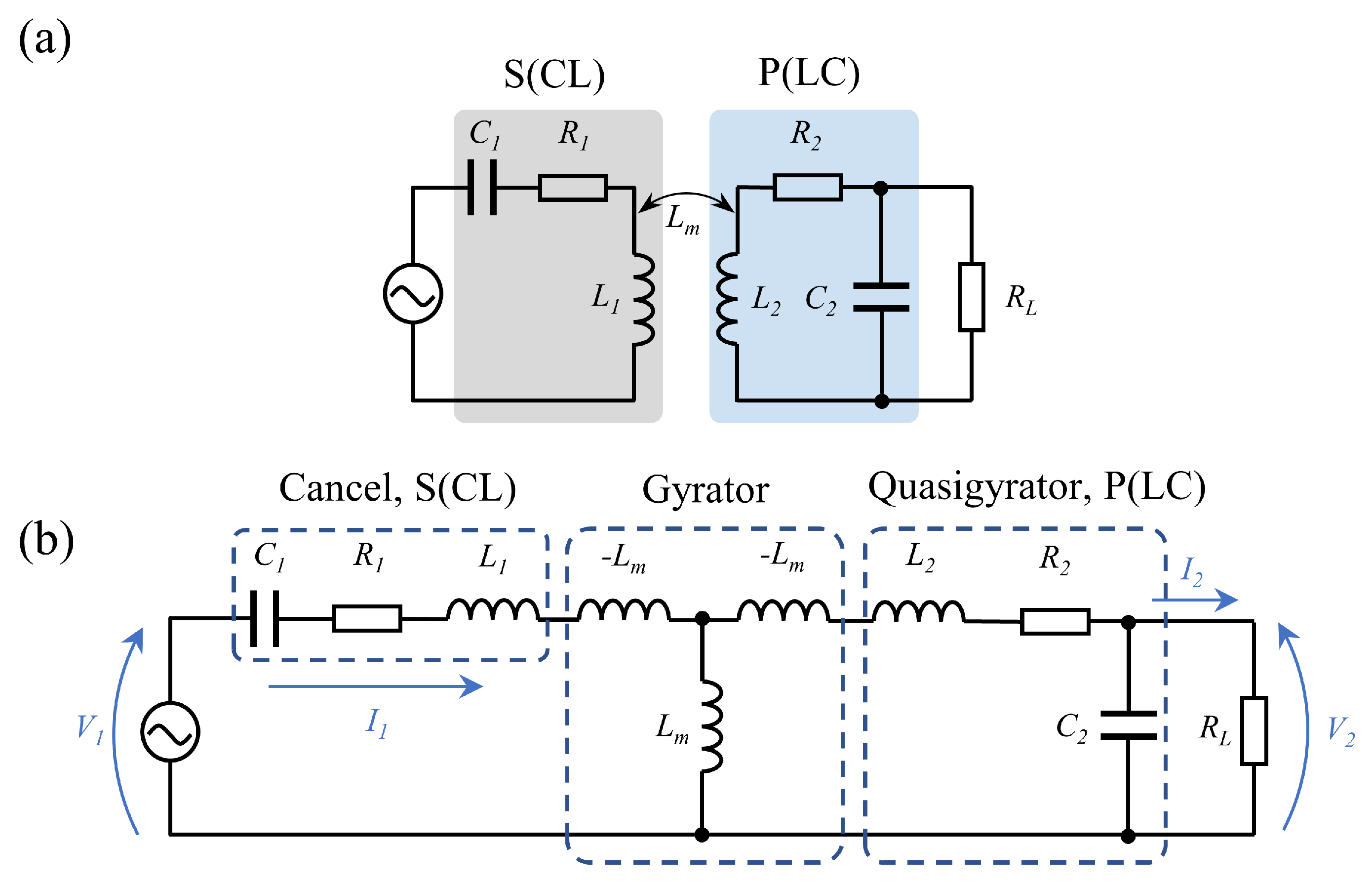
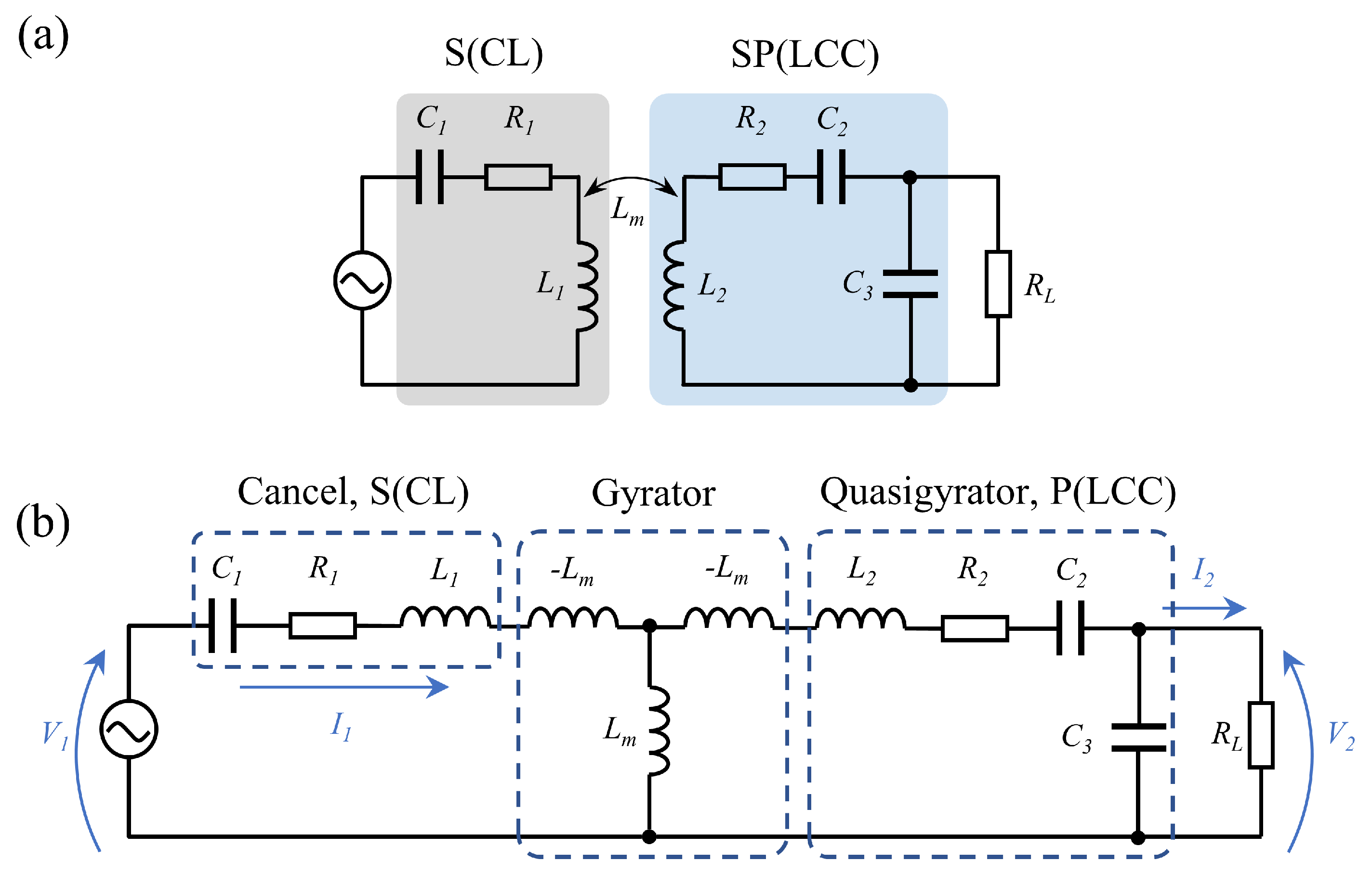
2.1. Parameter Analysis of the Wireless Power Transfer System

Bioimplants are usually implanted with several millimeter-diameter coils; the coupling coefficient between the coils is small so that the optimal load impedance of the wireless power link is usually around a few ohms. To reduce the equivalent load impedance, the primary side in series and the secondary side in parallel (S–P) topology is usually adopted, as shown in Figure 2.
We used the gyroscope theory to calculate the transfer function of S–P topology; V 1 and I 1 represent the input voltage and current, V 2 and I 2 represent the voltage and current output to the load [32,33,34]. To intuitively show the relationship between input and output and its influencing factors, we did not consider the internal resistances of the transmitter and receiver coil [24,35]. The transfer function is shown as:
V 1 I 1 = 0 j ω L m 1 j ω L m 0 · 0 j ω L 2 j ω C 2 1 · V 2 I 2 = ω 2 L m C 2 j ω L m 0 L 2 L m · V 2 I 2 = L m L 2 j ω L m 0 L 2 L m · V 2 I 2 ,
where I 2 = V 2 / R L , according to Equation (1), the relationship between output voltage and input voltage can be obtained in Equation (2):
V 2 V 1 = L 2 R L R L · L m j ω L 2 L m .
When the primary side uses a constant voltage source as input, the secondary side can be seen as a constant voltage source output. When the coil parameters are fixed, the output voltage gain is affected by the load resistance R L .
Considering the use of an ideal rectifier and voltage regulator, when DC-DC is used to adjust the output voltage, the load can be regarded as a constant power load, thus the equivalent load resistance from the DC-DC input side is R L = V 2 2 / P L . Let us consider the influence of input voltage variation on the output voltage. The voltage gain is shown as V 2 / V 1 = g s p . When the input voltage changes by a times, the input voltage is a · V 1 . Since the input voltage change will cause the voltage gain change, in this case, the voltage gain is expressed as g s p . The variation of secondary voltage is shown in Equation (3), and the variation of receiver equivalent load due to the variation of secondary side voltage V 2 is shown in Equation (4).
a · V 1 g s p · a · V 2
R L = g s p · a 2 · R L .
Substitute Equation (4) into Equation (2) to obtain the changed voltage gain g S P as shown in Equation (5).
g s p = 4 j ω L m 2 a 2 R L + L 2 2 + L 2 2 L m .
According to Equations (4) and (5), when the S–P structure has DC-DC for the output voltage regulator, the equivalent load impedance and voltage gain change non-linearly with the primary side voltage and bring two aspects of impact:
1. The variation of the secondary side equivalent load resistance makes the parallel equivalent resistance and the primary side reflected resistance change. The parallel equivalent impedance Z C R is represented by Equation (6), where R C R represents the real part and j X C R represents the imaginary part, as shown in Equations (7) and (8).
Z C R = R L / / 1 j ω C 2 = R C R + j X C R
R C R = R L 1 + ω 2 C 2 2 R L 2
j X C R = j ω C 2 R L 2 1 + ω 2 C 2 2 R L 2 .
Without considering the internal resistance of the transmitter and receiver coils, the reflected impedance Z r e f l at the primary side is represented by Equation (9).
Z r e f l = ω 2 L m 2 R C R = ω 2 L m 2 1 + ω 2 C 2 2 R L 2 R L .
In the S–P topology, R L changes to R L when the primary side voltage change, the reflection impedance change to Z r e f l s p , as shown in Equation (10).
Z r e f s p = ω 2 L m 2 1 + ω 2 C 2 2 g s p a 4 R L 2 g s p a 2 R L .
It can be seen from Equation (10) that adjusting the primary side voltage V 1 causes the nonlinear change of the reflected impedance, which makes the calculation of the secondary side voltage output by the current at the primary side become difficult. In actual use, due to the voltage division caused by the coils and power source, the change of the load impedance will further affect the accurate calculation of the output voltage.
2. The change of the imaginary part causes the off-resonance of the secondary side and reduces efficiency. For parallel resonance on the secondary side, the resonance condition is represented by Equation (11).
j ω L 2 + j X C R = 0 .
When the primary side voltage changes, the imaginary part of the parallel equivalent impedance is represented by Equation (12).
j X C R s p = j ω C 2 g s p a 4 R L 2 1 + ω 2 C 2 2 g s p a 4 R L 2 .
According to Equation (12), when the load impedance changes greatly, there is a risk of frequency mismatch at the secondary, which affects the voltage gain and reduces the efficiency. Z R represents the residual inductance or residual capacitance caused by the change of load resistance, and the efficiency of the receiver is expressed by Equation (13).
η 2 s p = R C R s p R C R s p + Z R .
The efficiency of the secondary side is reduced and the reactive power component is increased, so the transmit voltage needs to be further increased to achieve the power consumption required by the load. The increase of the transmitter voltage increases the SAR and endangers biological safety.
The load resistance can be matched through the reactive power matching network, which makes the equivalent load resistance closer to the optimal load impedance [25,36]. The topology formed by adding series capacitors is usually called S–SP topology, as shown in Figure 3.
Similarly, the gyroscope theory was used for analysis, and the S–SP structural transfer function was obtained as shown in Equation (14).
V 1 I 1 = 0 j ω L m 1 j ω L m 0 · 0 j ω L 2 + 1 j ω C 2 j ω C 3 1 · V 2 I 2 = ω 2 L m C 3 j ω L m 0 L 2 L m 1 ω 2 C 2 L m · V 2 I 2 = L m L 2 · C 2 + C 3 C 2 j ω L m 0 L 2 L m · C 2 C 2 + C 3 · V 2 I 2 .
When using a constant voltage source input, it is similar to the S–P structure and the output has similar constant voltage source characteristics, and I 2 = V 2 / R L ; the voltage gain is given by Equation (15).
V 2 V 1 = L 2 R L R L · L m C 2 + C 3 C 2 j ω L 2 L m .
V 2 / V 1 = g s s p represents the voltage gain of the S–SP topology. By comparing Equations (2) and (15), it can be seen that with the same coil parameters and load resistance, the voltage gain decreases as g s s p < g s p due to the capacitive voltage divider. Δ R L = R L R L represents the load variation at the secondary side due to input voltage variation. Compared with S–P topology, S–SP topology brings less load impedance variation, that is, Δ R L s s p < Δ R L s p . Thus the parallel equivalent impedance variation caused by the load impedance variation at the receiver is reduced Δ R C R s s p < Δ R C R s p , the resulting secondary side frequency mismatch is reduced as Δ j X C R s s p < Δ j X C R s p , and the reflected impedance variation is also reduced as Δ Z r e f l s s p < Δ Z r e f l s p .
It can be seen from the above analysis that the reduction of the load change makes the wireless power transfer link more stable and the change of the reflected impedance is also reduced.

2.2. An LDO-Based Linear-Power-Regulated Wireless Power Transfer Method

For the further reduction of the load resistance change caused by the primary side input voltage change, and to improve the stability and control accuracy of the wireless power transfer, we considered using LDO as the voltage controller on the secondary side as shown in Figure 4.
The following is a detailed analysis of its impact on wireless power transfer. Since the excess power will be consumed by the LDO, the power consumed by LDO is P L D O = V i n V o u t · I o u t , when the output voltage is V o u t , the output power is P o u t = V o u t · I o u t and the secondary side load consumes power is P = P L D O + P o u t , so the equivalent load resistance is R L = V i n / I o u t . Let the voltage gain as V 2 / V 1 = g , when the transmitter voltage V 1 changes, the equivalent load resistance R L change to R L , as shown in Equations (16) and (17).
a · V 1 g · a · V 2
a · V 1 g · a · V 2 .
Therefore, when LDO is used to adjust the output voltage in the S–SP topology, the resistance change at the secondary side can be represented by Equation (18).
Δ R L L D O = 1 g · a · R L .
When DC-DC is used to adjust the output voltage, the resistance change at the secondary side is shown in Equation (19).
Δ R L D C D C = 1 g · a 2 · R L .
It can be seen that Δ R L L D O < Δ R L D C D C , and the change of the resistance is linearly related to the change of the primary side voltage. Therefore, it can be known when the input voltage changes, the change of the load resistance is reduced, and the changes of the parameters of the wireless power system such as Δ R C R , Δ j X C R , Δ Z r e f l , are further reduced. By substituting Equation (17) into Equation (15), the voltage gain can be obtained as Equation (20).
g = L 2 L m + j ω L 2 a R L .
The voltage gain is changed from nonlinear variation to linear variation when LDO is used. The above analysis results show that the use of LDO to adjust the output voltage can further reduce variation of the resonant frequency, the parallel equivalent impedance and the reflection impedance, which provides the possibility for the primary side to precisely control the secondary side output voltage.
We performed simulations using Ansys Electronics Desktop Software with an ideal DC-DC and LDO. The load worked at 3.3 V output, 500 Ω load, and approximately 20 mW power. The simulation results are shown in Figure 5. It can be seen that the S–SP topology further reduces the equivalent load resistance in Figure 5a and the state change of the receiver in Figure 5c when the input voltage changes. However, the overall efficiency varies greatly with the input voltage, which is owing to the additional power loss caused by the residual capacitance at the receiver. Using LDO significantly reduces the voltage gain variation compared with using DC-DC, and maintains a relatively stable voltage gain when the input voltage varies greatly.

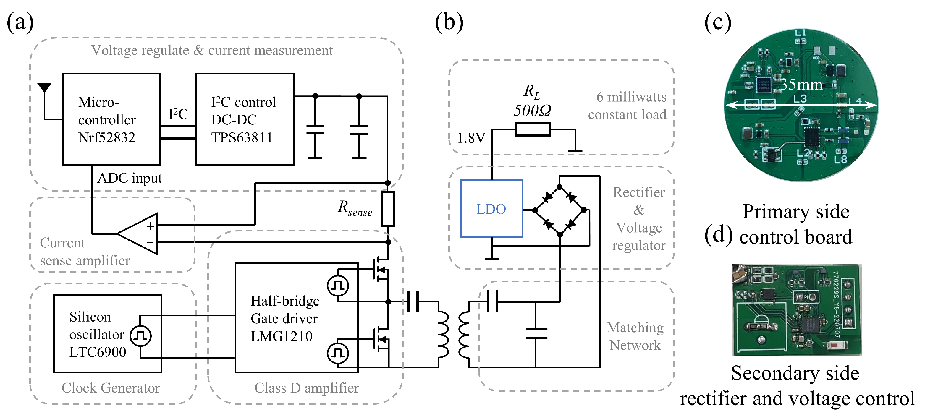
2.3. A Miniaturized Linear-Power-Regulated Wireless Power Transfer System

To verify the proposed method of using LDO to realize the parameter of the wireless power transfer system variation linearly, we developed a miniaturized linear-power-regulated wireless power transfer system as shown in Figure 6. The primary side system uses a silicon oscillator (LTC6900, Analog Devices, Inc., Wilmington, MA, USA) to generate a square wave signal with 13.56 MHz frequency, which is supplied to the half-bridge driver (LMG1210, Texas Instruments Inc., Dallas, TX, USA), combined with two GaN MOSFETs (EPC8010, Efficient Power Conversion Corporation, El Segundo, CA, USA) form a Class D amplifier. Because GaN Mosfet has a fast switching speed and the characteristics of low on-resistance, the use of GaN Mosfet has been shown to improve the efficiency of wireless power transfer systems [37]. This Class D amplifier connects to the series resonant capacitor and transmitting coil. The output voltage of the DC-DC (TPS63811, Texas Instruments Inc., Dallas, TX, USA) can be adjusted by the microcontroller (nRF52832, Nordic Semiconductor Inc., Trondheim, Norway) through the I 2 C bus, which can be adjusted by a 0.2 mV step. Compared with the method of adjusting DC-DC output voltage by DAC, the output voltage regulation is more accurate. The DC-DC output was connected to the input terminal of the Class D Amplifier and used base amplitude modulation to adjust the output voltage of wireless power transfer. A 100 m Ω current sampling resistor was connected in series with the DC-DC output, and a current detection amplifier (INA216, Texas Instruments Inc., Dallas, TX, USA) was used to convert the current value into a voltage value and input it to the internal ADC of the microcontroller to measure the output current.
The secondary side matched the load impedance by adding a series capacitor, and formed the S–SP wireless power transfer topology together with the primary side. The received energy was rectified using a full-bridge rectifier consisting of four Schottky diodes (RB161QS, ROHM Semiconductor, Shanghai, China) with a maximum 0.6 V voltage drop. The rectified voltage was regulated through a low quiescent current 1.8 V output LDO (TPS78218, Texas Instruments Inc., Dallas, TX, USA) and connected to a 500 Ω resistor as a load. The 1.8 V voltage drop usually conforms to the actual working voltage of the miniaturized brain–computer interface chip.
The transmitter coil and receiver coil were simulated by Ansys HFSS. By adjusting the coil size, the coil performance parameters obtained by Ansys HFSS simulation were consistent with those used in wireless power supply simulation. The inductance of the transmitting coil was about 1.5 μ H and the resistance was 160 m Ω . The inductance of the receiving coil was 800 nH and the resistance was 100 m Ω . The mutual inductance was about 400 nH in the distance of 5 mm full alignment; the specific parameters are shown in Table 1.

3. Results

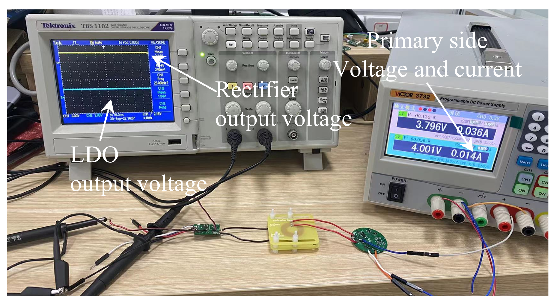
3.1. Measurement of Linear-Power-Regulated Wireless Power Transfer System

The test environment is shown in Figure 7. The oscilloscope was used to measure the rectifier output voltage and LDO output voltage at the secondary side. Because the I 2 C control DC-DC in this system can only output a voltage of 1.8–5.5 V, it can only generate a sine wave signal with a maximum amplitude of 5.5/2 × 4/ π = 3.5 V with the Class D Amplifier. To expand the measurement range, we used an external voltage source to achieve a wider range of primary side voltage variations. The primary side current is displayed through the voltage source.
The test results of voltage gain and primary side current are shown in Figure 8. The input voltage was adjusted by 0.2 V step between 4–10 V, and the output voltage after rectification was measured by oscilloscope. The secondary side measured output voltage value was multiplied by 2 to obtain the amplitude of the fundamental wave, and the primary side input voltage V 2 /2 × 4/ π to obtain the amplitude of the input fundamental wave. The ratio of output to the input voltage is shown on the left axis of Figure 8a. As the input voltage changes, the voltage gain remains almost constant. However, when the input voltage is high, the voltage gain starts to decrease. There are two reasons for the decrease in voltage gain:
1. As the primary side voltage increases, the power consumption of the circuit increases, which makes the temperature of the circuit increase, therefore resulting in a decrease in voltage gain;
2. When the LDO is used to adjust the output voltage, the current at the secondary side increases synchronously with the primary side voltage, resulting in an increased voltage drop of the rectifier. Make the measured output voltage decrease after rectification.
The current at the transmitter is shown on the right axis. As the input voltage changes, the current linearly increases, indicating that the reflected impedance at the transmitter can be kept stable when LDO is used to adjust the output voltage.
Figure 8b shows the measurement results after the coils are offset by 5 mm. The mutual inductance L m decreases. According to Equations (14) and (15), the voltage gain increases because the ratio of L 2 to L m increases. As the mutual inductance decreases, the reflected impedance decreases, so the primary side current increases. The voltage gain decline is more serious; this is due to the decreased coupling coefficient makes the primary side need to provide more energy, and the loss in the primary side increases.

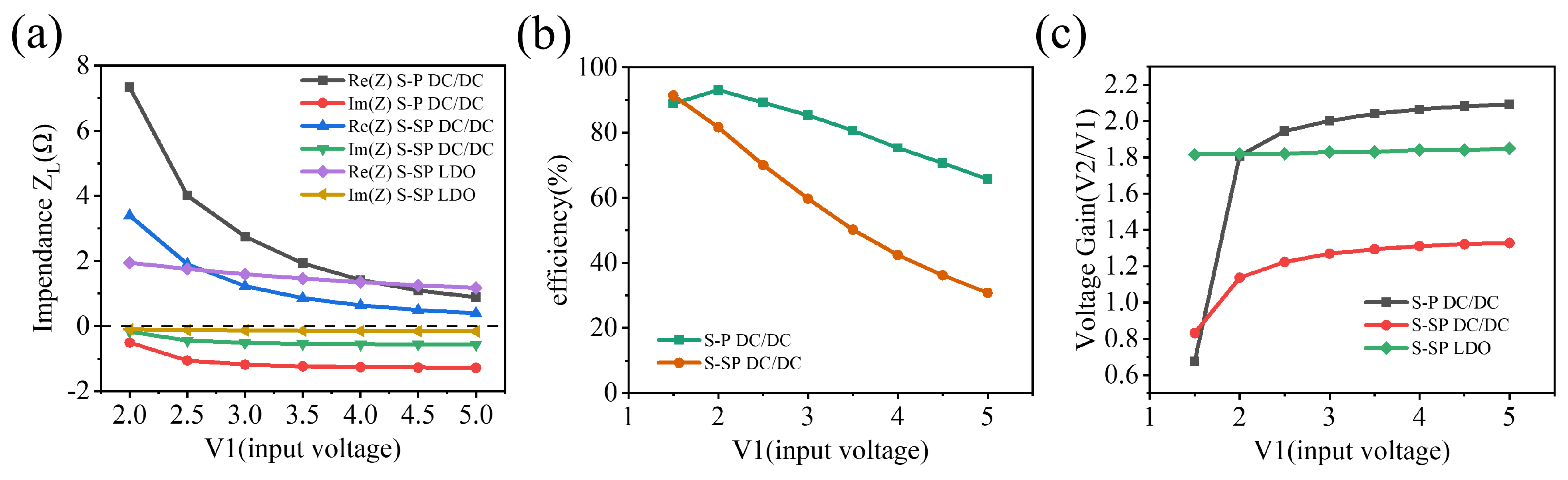
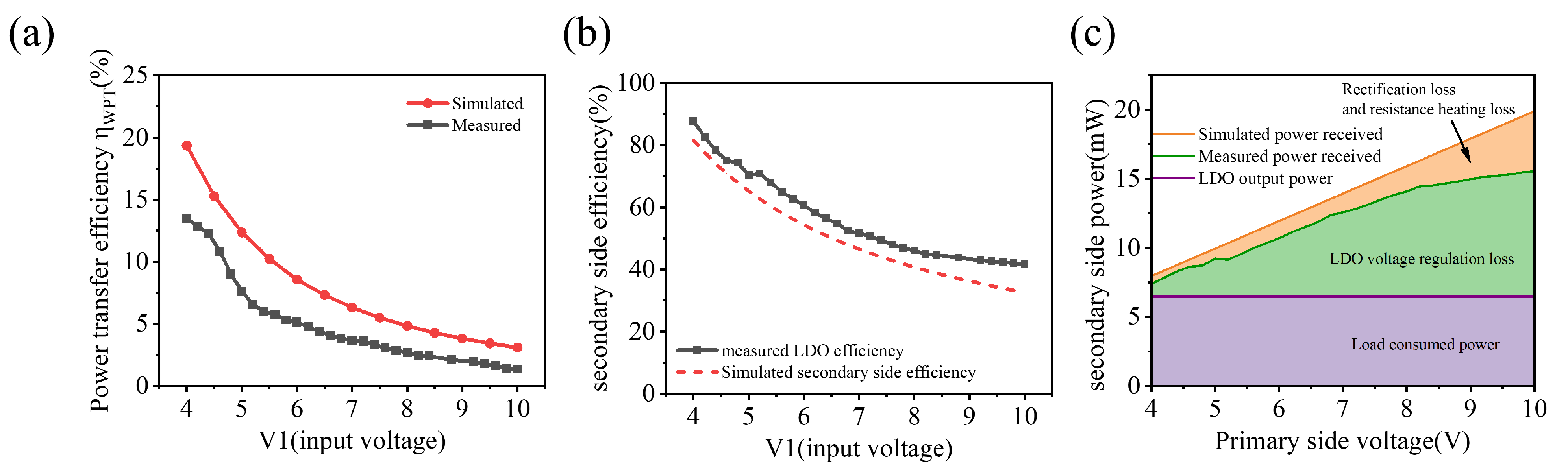
3.2. Measurement and Analysis of Wireless Power Transfer Efficiency

The overall efficiency of the wireless power transfer system and the partial secondary side efficiency are shown in Figure 9. Figure 9a shows the overall efficiency of the wireless power transfer system. As the input voltage of LDO is much higher than the output voltage when the voltage changes greatly, LDO consumes a large amount of energy, so the efficiency decreases greatly. The actual test results are lower than the simulation results, but keep the same trend as the simulation results.
Figure 9b,c show the efficiency of the secondary side and the analysis of the power consumed. The simulation results show that the receiver efficiency can reach more than 80% when the output voltage after rectification is controlled to be close to the output voltage of LDO. When the LDO input voltage is significantly higher than the LDO output voltage, the loss generated by the LDO and the loss of the rectifier bridge increase synchronously. The voltage drop of the Schottky diode is linearly related to the current flowing through it. Therefore, in the application of low-power implants, the rectifier bridge loss is extremely low. Even if the Schottky diode with the highest voltage drop of 0.6 V is selected, the voltage drop generated by the Schottky diode in the actual test is below 0.3 V. By selecting an ultra-low voltage drop Schottky diode of up to 0.2 V, the bridge loss will be further reduced, allowing the receiver efficiency to reach more than 90%. It is much higher than the receiver efficiency of about 70% when the output voltage is regulated by DC-DC. Therefore, the use of LDO to regulate the output voltage will significantly reduce the heat dissipation in the organism caused by the wireless power transfer, which is conducive to reducing the impact on the neural activity of the organism.

4. Discussion

By analyzing the transfer function of the wireless power transfer system, we determined that the load impedance change is the main factor affecting the state of the wireless power transfer when the primary side voltage is changed. In the existing structure, DC-DC is generally used to adjust the output voltage, so that the wireless power transfer system has the strong robust performance to cope with the possible large changes in the coupling coefficient. However, the equivalent load resistance is a non-linear change with the primary side input voltage, causing the nonlinear variation of the resonant frequency and the reflected impedance. The efficiency of on-chip DC-DC is usually less than 70% under low power conditions; the impact of the resulting heating dissipation in the living body is difficult to measure.
When LDO is used to adjust the output voltage, the load impedance change can be from a nonlinear to a linear change and reduces the change amount. When using LDO, it is necessary to strictly control the rectified output voltage to keep the efficiency of the LDO above 90%. Since the change of the reflected impedance is reduced, the change of the coupling coefficient can be calculated and the output voltage can be accurately adjusted. The actual test shows that the efficiency of the secondary side is above 80% when using LDO, and when the rectified output voltage is closer to the LDO output voltage, the efficiency will be further improved. Compared with the use of DC-DC to adjust the output voltage, the use of LDO greatly improves the efficiency of the secondary side, and significantly reduces the heat dissipation in the living body. Moreover, LDO is easier to integrate on-chip, and its small area and low noise features are more conducive to applications such as neural recording. The comparison of on-chip LDO and DC-DC in wireless power transfer is shown in Table 2.
As far as the rectifier loss is concerned, when using DC-DC as a power regulator, the rectifier bridge loss can be reduced by increasing the voltage output. Since the voltage drop caused by the rectifier changes linearly with the flowing current, in the application of implanted devices, due to the low current, the actual test found that the loss caused by the rectifier bridge is extremely low, so it is not particularly important to optimize the efficiency of the rectifier. The selection of ultra-low drop Schottky diodes, semi-active rectifier circuits, or voltage doubler rectifier circuits will further reduce the loss of the rectifier.
In recent years, distributed multi-node brain–computer interface implants have emerged [41,42]. Compared with the use of DC-DC, LDO is more limited in these applications, as the energy transmitted to each implant needs to be independently controlled to maintain the high efficiency of the secondary side. A novel wireless power transfer metasurface will possibly solve this problem [12,43,44,45]. By detecting the reflection resistance generated by each implant and automatically distributing the power transmitted to each implant, the overall efficiency of the wireless power transfer system can be improved while maintaining the high efficiency of each implant.

5. Conclusions

We propose a linear-power-regulated wireless power transfer method for decreasing the heat dissipation of fully implantable microsystems in this paper. With the LDO on the secondary side, the parameters of the wireless power transfer system change linearly in the power control process. An LDO-based linear-power-regulated wireless power transfer system was developed and tested; the secondary side efficiency can reach more than 80% with the primary side voltage control, which is significantly improved compared with the use of DC-DC to regulate the output voltage and can effectively reduce the heat dissipation in the organism. The linear-power-regulated wireless power transfer method can reduce the dependence on wireless communication in optimal efficiency tracking applications and improve biological safety.

Author Contributions

Conceptualization, H.W., C.Z. and H.H.; methodology, H.W., K.C. and H.H.; software, W.J. and J.T.; validation, H.W., C.Z. and H.H.; formal analysis, K.C. and H.H.; investigation, H.W., K.C. and H.H.; resources, K.C. and H.H.; data curation, Z.W., J.T. and W.J.; writing—original draft preparation, H.W.; writing—review and editing, Z.W. and H.H.; visualization C.Z.; supervision, K.C., Z.W. and H.H.; project administration, K.C. and H.H.; funding acquisition, K.C. and H.H. All authors have read and agreed to the published version of the manuscript.

Funding

This research was funded by the “Pioneer” and “Leading Goose” R&D Program of Zhejiang under Grant 2022C01119; National Natural Science Foundation of China under Grant 62171169.

Institutional Review Board Statement

Not applicable.

Informed Consent Statement

Not applicable.

Data Availability Statement

Not applicable.

Acknowledgments

The authors would like to thank Lingling Qi of Nokia Communication System Technology for her help with the wireless power transfer method and system construction.

Conflicts of Interest

The authors declare no conflict of interest.

Abbreviations

The following abbreviations are used in this manuscript:
FCCFederal Communications Commission
SARSpecific absorption rate
BCIBrain-computer interfaces
WPTWireless power transfer

References

  1. Luan, L.; Robinson, J.T.; Aazhang, B.; Chi, T.; Yang, K.; Li, X.; Rathore, H.; Singer, A.; Yellapantula, S.; Fan, Y.; et al. Recent advances in electrical neural interface engineering: Minimal invasiveness, longevity, and scalability. Neuron 2020, 108, 302–321. [Google Scholar] [CrossRef]
  2. Yan, T.; Kameda, S.; Suzuki, K.; Kaiju, T.; Inoue, M.; Suzuki, T.; Hirata, M. Minimal Tissue Reaction after Chronic Subdural Electrode Implantation for Fully Implantable Brain–Machine Interfaces. Sensors 2020, 21, 178. [Google Scholar] [CrossRef] [PubMed]
  3. Mutlu, S. Challenges in Neural Interface Electronics: Miniaturization and Wireless Operation. In Somatosensory Feedback for Neuroprosthetics; Elsevier: Amsterdam, The Netherlands, 2021; pp. 537–559. [Google Scholar]
  4. Yang, K.W.; Oh, K.; Ha, S. Challenges in scaling down of free-floating implantable neural interfaces to millimeter scale. IEEE Access 2020, 8, 133295–133320. [Google Scholar] [CrossRef]
  5. Jin, P.; Fu, J.; Wang, F.; Zhang, Y.; Wang, P.; Liu, X.; Jiao, Y.; Li, H.; Chen, Y.; Ma, Y.; et al. A flexible, stretchable system for simultaneous acoustic energy transfer and communication. Sci. Adv. 2021, 7, eabg2507. [Google Scholar] [CrossRef] [PubMed]
  6. Dinis, H.; Mendes, P. A comprehensive review of powering methods used in state-of-the-art miniaturized implantable electronic devices. Biosens. Bioelectron. 2021, 172, 112781. [Google Scholar] [CrossRef] [PubMed]
  7. Kim, C.Y.; Ku, M.J.; Qazi, R.; Nam, H.J.; Park, J.W.; Nam, K.S.; Oh, S.; Kang, I.; Jang, J.H.; Kim, W.Y.; et al. Soft subdermal implant capable of wireless battery charging and programmable controls for applications in optogenetics. Nat. Commun. 2021, 12, 535. [Google Scholar] [CrossRef]
  8. Jia, Y.; Mirbozorgi, S.A.; Lee, B.; Khan, W.; Madi, F.; Inan, O.T.; Weber, A.; Li, W.; Ghovanloo, M. A mm-sized free-floating wirelessly powered implantable optical stimulation device. IEEE Trans. Biomed. Circuits Syst. 2019, 13, 608–618. [Google Scholar] [CrossRef] [PubMed]
  9. Bailey, W.H.; Bodemann, R.; Bushberg, J.; Chou, C.K.; Cleveland, R.; Faraone, A.; Foster, K.R.; Gettman, K.E.; Graf, K.; Harrington, T.; et al. Synopsis of IEEE Std C95.1TM-2019 “IEEE Standard for Safety Levels With Respect to Human Exposure to Electric, Magnetic, and Electromagnetic Fields, 0 Hz to 300 GHz”. IEEE Access 2019, 7, 171346–171356. [Google Scholar] [CrossRef]
  10. Code, S. Limits of Human Exposure to Radiofrequency Electromagnetic Energy in the Frequency Range from 3 khz to 300 ghz; Health Canada: Ottawa, ON, Canada, 2015. [Google Scholar]
  11. Park, J.; Kim, C.; Akinin, A.; Ha, S.; Cauwenberghs, G.; Mercier, P.P. Wireless Powering of MM-Scale Fully-on-Chip Neural Interfaces. In Proceedings of the 2017 IEEE Biomedical Circuits and Systems Conference (BioCAS), Torino, Italy, 19–21 October 2017; pp. 1–4. [Google Scholar]
  12. Markvart, A.; Song, M.; Glybovski, S.; Belov, P.; Simovski, C.; Kapitanova, P. Metasurface for near-field wireless power transfer with reduced electric field leakage. IEEE Access 2020, 8, 40224–40231. [Google Scholar] [CrossRef]
  13. Huang, Z.; Wong, S.C.; Chi, K.T. Comparison of basic inductive power transfer systems with linear control achieving optimized efficiency. IEEE Trans. Power Electron. 2019, 35, 3276–3286. [Google Scholar] [CrossRef]
  14. Zhang, W.; Wong, S.C.; Chi, K.T.; Chen, Q. Load-independent duality of current and voltage outputs of a series-or parallel-compensated inductive power transfer converter with optimized efficiency. IEEE J. Emerg. Sel. Top. Power Electron. 2014, 3, 137–146. [Google Scholar] [CrossRef]
  15. Schormans, M.; Valente, V.; Demosthenous, A. Practical inductive link design for biomedical wireless power transfer: A tutorial. IEEE Trans. Biomed. Circuits Syst. 2018, 12, 1112–1130. [Google Scholar] [CrossRef] [Green Version]
  16. Shevchenko, V.; Husev, O.; Strzelecki, R.; Pakhaliuk, B.; Poliakov, N.; Strzelecka, N. Compensation topologies in IPT systems: Standards, requirements, classification, analysis, comparison and application. IEEE Access 2019, 7, 120559–120580. [Google Scholar] [CrossRef]
  17. Miura, N.; Kodera, S.; Diao, Y.; Higashiyama, J.; Suzuki, Y.; Hirata, A. Power absorption and skin temperature rise from simultaneous near-field exposure at 2 and 28 GHz. IEEE Access 2021, 9, 152140–152149. [Google Scholar] [CrossRef]
  18. Yang, Y.; Wu, M.; Vázquez-Guardado, A.; Wegener, A.J.; Grajales-Reyes, J.G.; Deng, Y.; Wang, T.; Avila, R.; Moreno, J.A.; Minkowicz, S.; et al. Wireless multilateral devices for optogenetic studies of individual and social behaviors. Nat. Neurosci. 2021, 24, 1035–1045. [Google Scholar] [CrossRef]
  19. Jia, Y.; Guler, U.; Lai, Y.P.; Gong, Y.; Weber, A.; Li, W.; Ghovanloo, M. A trimodal wireless implantable neural interface system-on-chip. IEEE Trans. Biomed. Circuits Syst. 2020, 14, 1207–1217. [Google Scholar] [CrossRef] [PubMed]
  20. Khalifa, A.; Liu, Y.; Karimi, Y.; Wang, Q.; Eisape, A.; Stanaćević, M.; Thakor, N.; Bao, Z.; Etienne-Cummings, R. The microbead: A 0.009 mm3 implantable wireless neural stimulator. IEEE Trans. Biomed. Circuits Syst. 2019, 13, 971–985. [Google Scholar] [CrossRef] [PubMed]
  21. Leene, L.B.; Maslik, M.; Feng, P.; Szostak, K.M.; Mazza, F.; Constandinou, T.G. Autonomous SoC for Neural Local Field Potential Recording in MM-Scale Wireless Implants. In Proceedings of the 2018 IEEE International Symposium on Circuits and Systems (ISCAS), Florence, Italy, 27–30 May 2018; pp. 1–5. [Google Scholar]
  22. Jia, Y.; Mirbozorgi, S.A.; Lee, B.; Khan, W.; Madi, F.; Weber, A.; Li, W.; Ghovanloo, M. A MM-Sized Free-Floating Wirelessly Powered Implantable Optical Stimulating System-on-a-Chip. In Proceedings of the 2018 IEEE International Solid-State Circuits Conference-(ISSCC), San Francisco, CA, USA, 11–15 February 2018; pp. 468–470. [Google Scholar]
  23. Ahire, D.; Gond, V.J.; Chopade, J.J. Compensation topologies for wireless power transmission system in medical implant applications: A review. Biosens. Bioelectron. X 2022, 11, 100180. [Google Scholar] [CrossRef]
  24. Imura, T. Wireless Power Transfer: Using Magnetic and Electric Resonance Coupling Techniques; Springer Nature: Berlin/Heidelberg, Germany, 2020. [Google Scholar]
  25. Zhang, W.; Wong, S.C.; Chi, K.T.; Chen, Q. Analysis and comparison of secondary series-and parallel-compensated inductive power transfer systems operating for optimal efficiency and load-independent voltage-transfer ratio. IEEE Trans. Power Electron. 2013, 29, 2979–2990. [Google Scholar] [CrossRef]
  26. Su, L.; Ma, D.; Brokaw, A.P. Design and analysis of monolithic step-down SC power converter with subthreshold DPWM control for self-powered wireless sensors. IEEE Trans. Circuits Syst. I Regul. Pap. 2009, 57, 280–290. [Google Scholar]
  27. Ciarpi, G.; Saponara, S. Inductorless DC/DC converter for aerospace applications with insulation features. IEEE Trans. Circuits Syst. II Express Briefs 2020, 67, 1659–1663. [Google Scholar] [CrossRef]
  28. Carreon-Bautista, S.; Erbay, C.; Han, A.; Sanchez-Sinencio, E. An inductorless DC–DC converter for an energy aware power management unit aimed at microbial fuel cell arrays. IEEE J. Emerg. Sel. Top. Power Electron. 2015, 3, 1109–1121. [Google Scholar] [CrossRef]
  29. Stoecklin, S.; Yousaf, A.; Gidion, G.; Reindl, L.; Rupitsch, S.J. Simultaneous power feedback and maximum efficiency point tracking for miniaturized rf wireless power transfer systems. Sensors 2021, 21, 2023. [Google Scholar] [CrossRef] [PubMed]
  30. Yeo, T.D.; Kwon, D.; Khang, S.T.; Yu, J.W. Design of maximum efficiency tracking control scheme for closed-loop wireless power charging system employing series resonant tank. IEEE Trans. Power Electron. 2016, 32, 471–478. [Google Scholar] [CrossRef]
  31. Li, H.; Li, J.; Wang, K.; Chen, W.; Yang, X. A maximum efficiency point tracking control scheme for wireless power transfer systems using magnetic resonant coupling. IEEE Trans. Power Electron. 2014, 30, 3998–4008. [Google Scholar] [CrossRef]
  32. Narusue, Y.; Kawahara, Y.; Asami, T. Variable-Hop Impedance Matching Method for Magnetic Resonance Based Wireless Power Transmission Relays; IEICE Technical Report; The Institute of Electronics, Information and Communication Engineers (IEICE): Tokyo, Japan, 2012. [Google Scholar]
  33. Koh, K.E.; Imura, T.; Hori, Y. Impedance Inverter Based Analysis of Wireless Power Transfer Consists of Repeaters via Magnetic Resonant Coupling; Technical Report, IEICE Technical Report, WPT2012-37; The Institute of Electronics, Information and Communication Engineers (IEICE): Tokyo, Japan, 2012. [Google Scholar]
  34. Koh, K.E.; Beh, T.C.; Imura, T.; Hori, Y. Impedance matching and power division using impedance inverter for wireless power transfer via magnetic resonant coupling. IEEE Trans. Ind. Appl. 2013, 50, 2061–2070. [Google Scholar] [CrossRef]
  35. Zhong, W.; Xu, D.; Hui, R.S.Y.; Xu, D.; Hui, R.S.Y. Wireless Power Transfer: Between Distance and Efficiency; Springer: Berlin/Heidelberg, Germany, 2020. [Google Scholar]
  36. Hou, J.; Chen, Q.; Yan, K.; Ren, X.; Wong, S.C.; Tse, C.K. Analysis and Control of S/SP Compensation Contactless Resonant Converter with Constant Voltage Gain. In Proceedings of the 2013 IEEE Energy Conversion Congress and Exposition, Denver, CO, USA, 15–19 September 2013; pp. 2552–2558. [Google Scholar]
  37. Iero, D.; Carotenuto, R.; Merenda, M.; Pezzimenti, F.; Della Corte, F.G. Performance Evaluation of Silicon and GaN Switches for a Small Wireless Power Transfer System. Energies 2022, 15, 3029. [Google Scholar] [CrossRef]
  38. Kao, S.K.; Chen, J.J.; Liao, C.H. A Multipath Output-Capacitor-Less LDO Regulator. IEEE Access 2022, 10, 27185–27196. [Google Scholar] [CrossRef]
  39. Guo, Z.; Li, D.; Zhang, B.; Xue, Z.; Dong, L.; Chen, Z.; Xiong, Y.; Geng, L. Highly Efficient Fully Integrated Multivoltage-Domain Power Management With Enhanced PSR and Low Cross-Regulation. IEEE Trans. Power Electron. 2021, 36, 11469–11482. [Google Scholar] [CrossRef]
  40. George, L.; Gargiulo, G.D.; Lehmann, T.; Hamilton, T.J. A 0.04 mm2 Buck-Boost DC-DC Converter for Biomedical Implants Using Adaptive Gain and Discrete Frequency Scaling Control. IEEE Trans. Biomed. Circuits Syst. 2015, 10, 668–678. [Google Scholar] [CrossRef]
  41. Lee, J.; Leung, V.; Lee, A.H.; Huang, J.; Asbeck, P.; Mercier, P.P.; Shellhammer, S.; Larson, L.; Laiwalla, F.; Nurmikko, A. Neural recording and stimulation using wireless networks of microimplants. Nat. Electron. 2021, 4, 604–614. [Google Scholar] [CrossRef]
  42. Mirbozorgi, S.A.; Yeon, P.; Ghovanloo, M. Robust wireless power transmission to mm-sized free-floating distributed implants. IEEE Trans. Biomed. Circuits Syst. 2017, 11, 692–702. [Google Scholar] [CrossRef]
  43. Smirnov, P.; Kapitanova, P.; Nenasheva, E.; Song, M. Compact Hybrid Metasurface-Inspired Resonator with Uniform Magnetic Field Distribution for Wireless Power Transfer. IEEE Antennas Wirel. Propag. Lett. 2021, 21, 193–197. [Google Scholar] [CrossRef]
  44. Cho, Y.; Lee, S.; Kim, D.H.; Kim, H.; Song, C.; Kong, S.; Park, J.; Seo, C.; Kim, J. Thin hybrid metamaterial slab with negative and zero permeability for high efficiency and low electromagnetic field in wireless power transfer systems. IEEE Trans. Electromagn. Compat. 2017, 60, 1001–1009. [Google Scholar] [CrossRef]
  45. Cho, Y.; Lee, S.; Jeong, S.; Kim, H.; Song, C.; Yoon, K.; Song, J.; Kong, S.; Yun, Y.; Kim, J. Hybrid Metamaterial with Zero and Negative Permeability to Enhance Efficiency in Wireless Power Transfer System. In Proceedings of the 2016 IEEE Wireless Power Transfer Conference (WPTC), Aveiro, Portugal, 5–6 May 2016; pp. 1–3. [Google Scholar]
Figure 1. Concept of the linear-power-regulated wireless power transfer system.
Sensors 22 08765 g001
Figure 2. Circuit model of the S−P topology WPT system. (a) System structure of S−P topology WPT system, (b) equivalent circuit of S−P topology.
Sensors 22 08765 g002
Figure 3. Circuit model of the S−SP topology WPT system. (a) System structure of S−SP topology WPT system, (b) equivalent circuit of S−SP topology.
Sensors 22 08765 g003
Figure 4. System structure of the secondary side voltage regulator and concept of the reflected impedance in the primary side.
Sensors 22 08765 g004
Figure 5. The simulated results of the WPT system. (a) The load equivalent impedance varies with the transmit voltage in S−P and S−SP typologies, (b) the variation of the WPT system efficiency with transmitting voltage, (c) the variation of voltage gain with transmitting voltage.
Sensors 22 08765 g005
Figure 6. Miniaturized linear-power-regulated wireless power transfer system. (a) Schematic of the miniaturized primary side power control system, (b) schematic of the LDO-based secondary side wireless power receiver system, (c) photograph of the miniaturized primary side power control board, (d) photograph of the secondary side wireless power receiver board.
Sensors 22 08765 g006
Figure 7. Measurement setup for the linear-power-regulated wireless power transfer system.
Sensors 22 08765 g007
Figure 8. Measurement results of the voltage gain in the power control process and the related primary side current. (a) Coils with 5 mm intervals and perfectly aligned, (b) Coils with 5 mm intervals and with 5 mm offset.
Sensors 22 08765 g008
Figure 9. Measurement results of the linear-power-regulated WPT system. (a) The power efficiency of the overall WPT system, (b) the power efficiency of the secondary side, (c) the analysis of the secondary side power consumption.
Sensors 22 08765 g009
Table 1. Coils specific parameters. Lm represents the mutual inductance of the two coils.
CoilTurnsDiameter (mm)Inductance (nH)Resistance (m Ω )Lm (nH)
transmitter9101500160400 (d = 5 mm)
receiver510800100
Table 2. The comparison of on-chip DC-DC and LDO as the secondary side voltage regulator.
TypeLDODC-DC
Reference[38][39][40][28][27]
Year20222021201520152020
Chip Area (mm 2 )0.1280.490.041.836
CMOS Process ( μ m)0.180.180.180.180.35
Input voltage (V)1.2–1.83.3–3.61.86–600.3–0.4
Output voltage (V)10.8–3.21.0–2.21.65, 51.6–2
Efficiency83% (max)96.5% (max)30–75%65% (max)40–65%
Publisher’s Note: MDPI stays neutral with regard to jurisdictional claims in published maps and institutional affiliations.

