
Energy-Efficient and Variability-Resilient 11T SRAM Design Using Data-Aware Read–Write Assist (DARWA) Technique for Low-Power Applications
Abstract
:1. Introduction
- A novel technique named Data-Aware Read–Write Assist (DARWA) is applied with single-ended read operation and dynamic differential write operation;
- The faster data switching happens when the latch circuit is totally disconnected at the nodes for write operations, which confirms lower dynamic power consumption due to lesser discharging at the bit lines (BL and BLB);
- The independent single-ended and separate read circuit performs a quicker read operation and hence reduces the read power consumption and enhances the read stability and overall read performance;
- The stack effect is introduced using tail transistors on both sides of the latch, which significantly minimizes the leakage power;
- The variability in the read, write, and hold modes is investigated and analyzed in detail to examine the resilience and robustness of the proposed cell using 5000 samples in Monte Carlo (MC) simulations.
2. Related Works
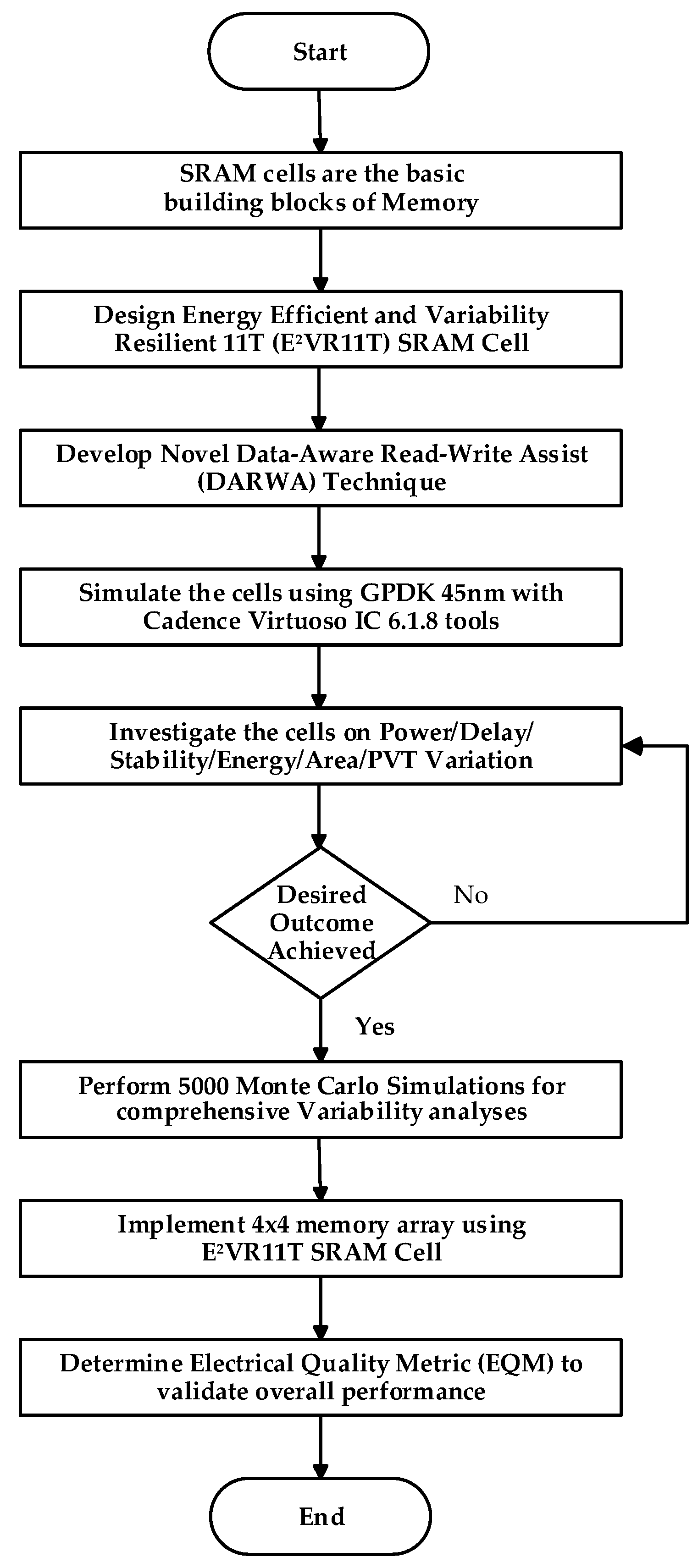
3. Materials and Methods
3.1. Data-Aware Read–Write Assist (DARWA) Technique
- Single-Ended Read Operation
- Dynamic Differential Write Operation
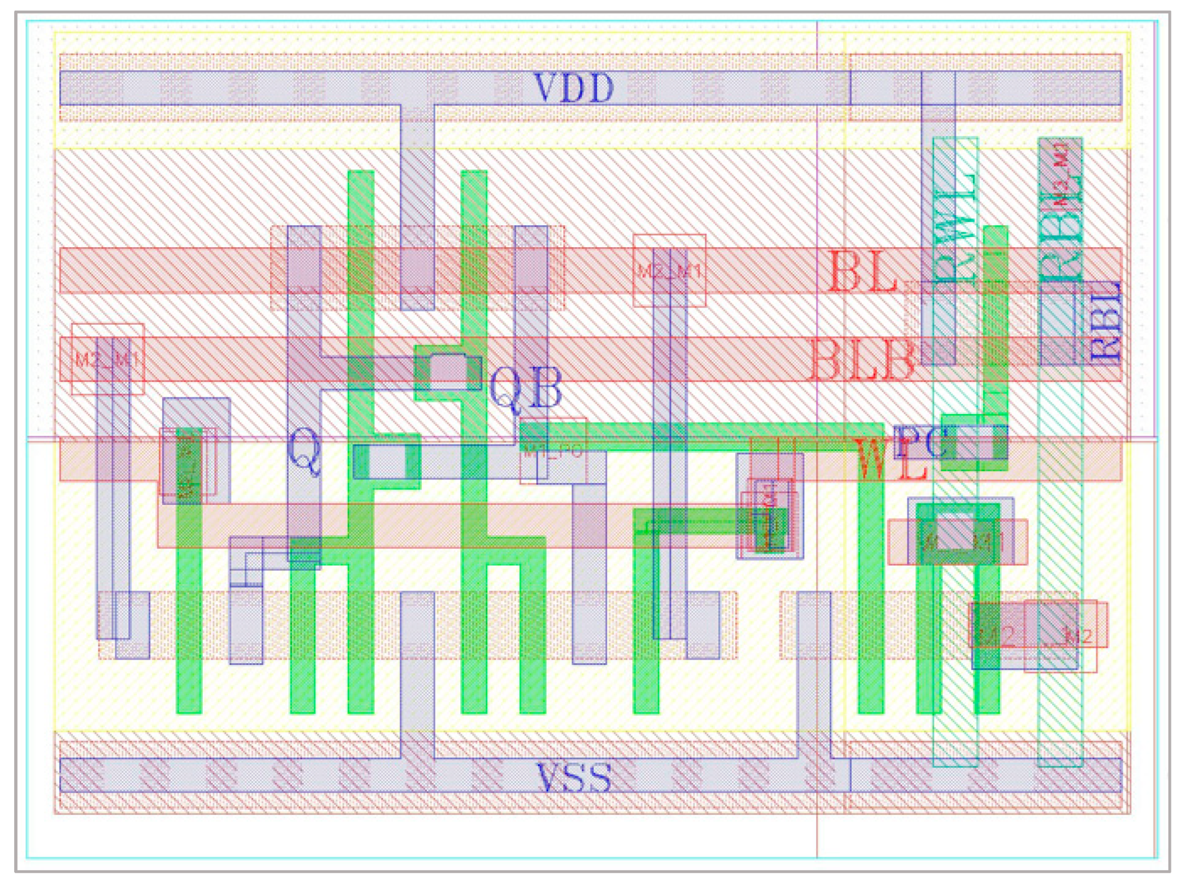
3.2. Design of Energy-Efficient and Variability-Resilient 11T (E2VR11T) SRAM Cell
3.3. Working Principle of E2VR11T SRAM Cell
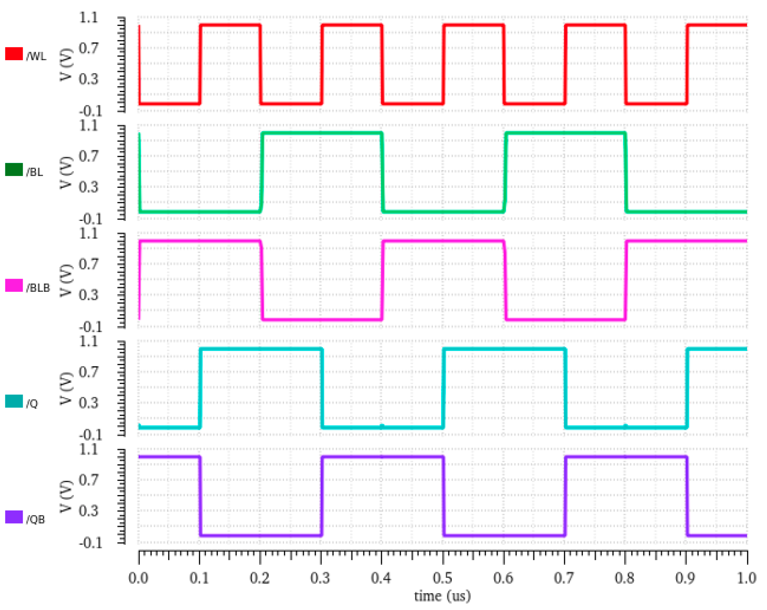
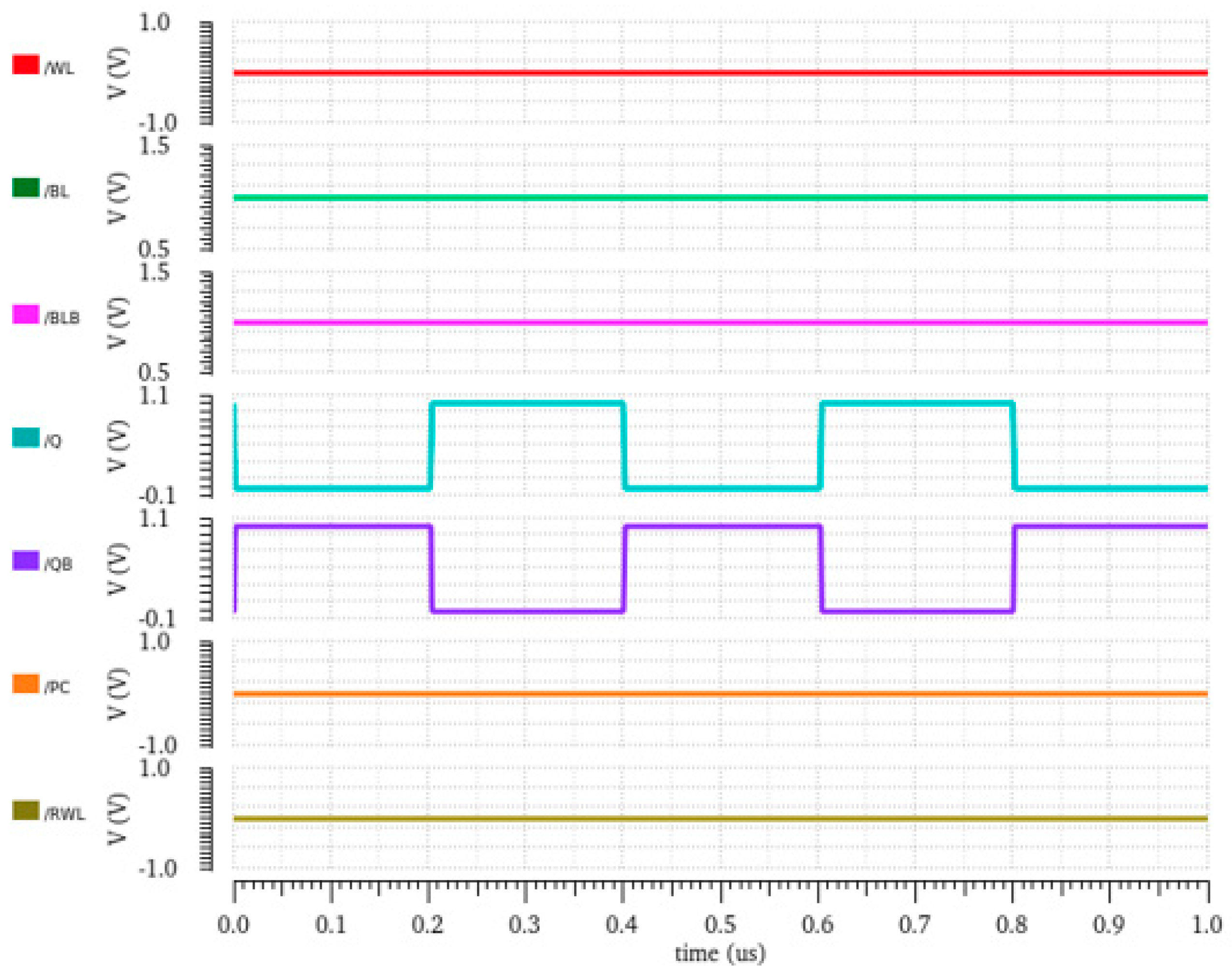
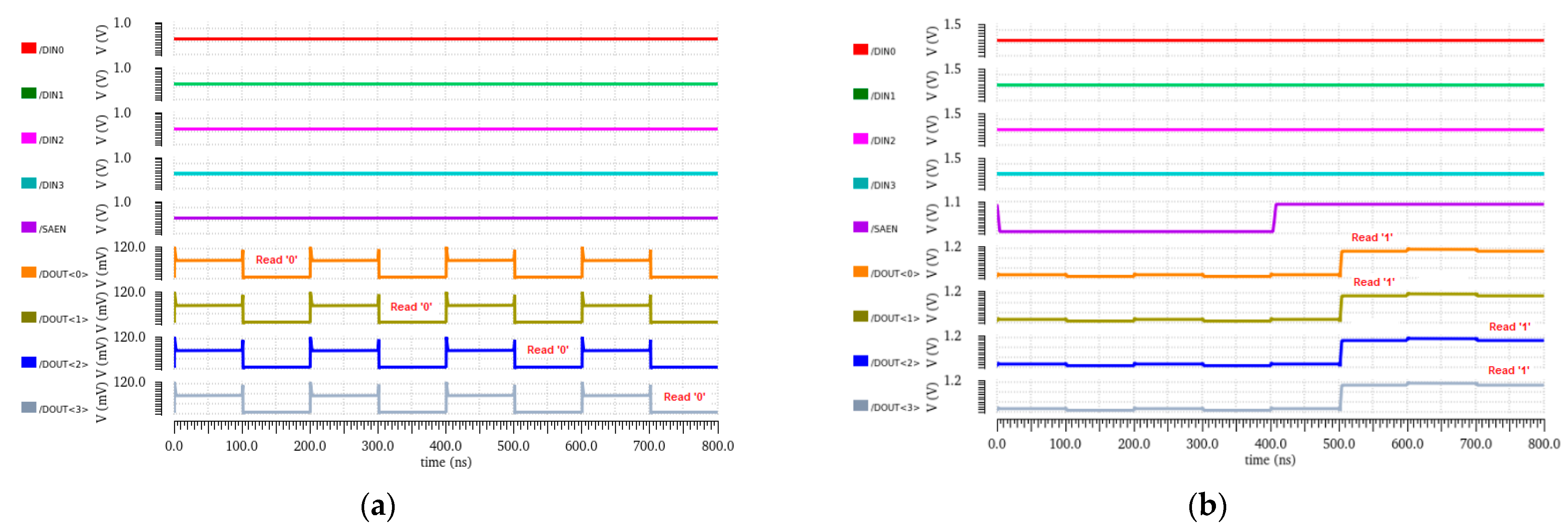
3.3.1. Read Operation
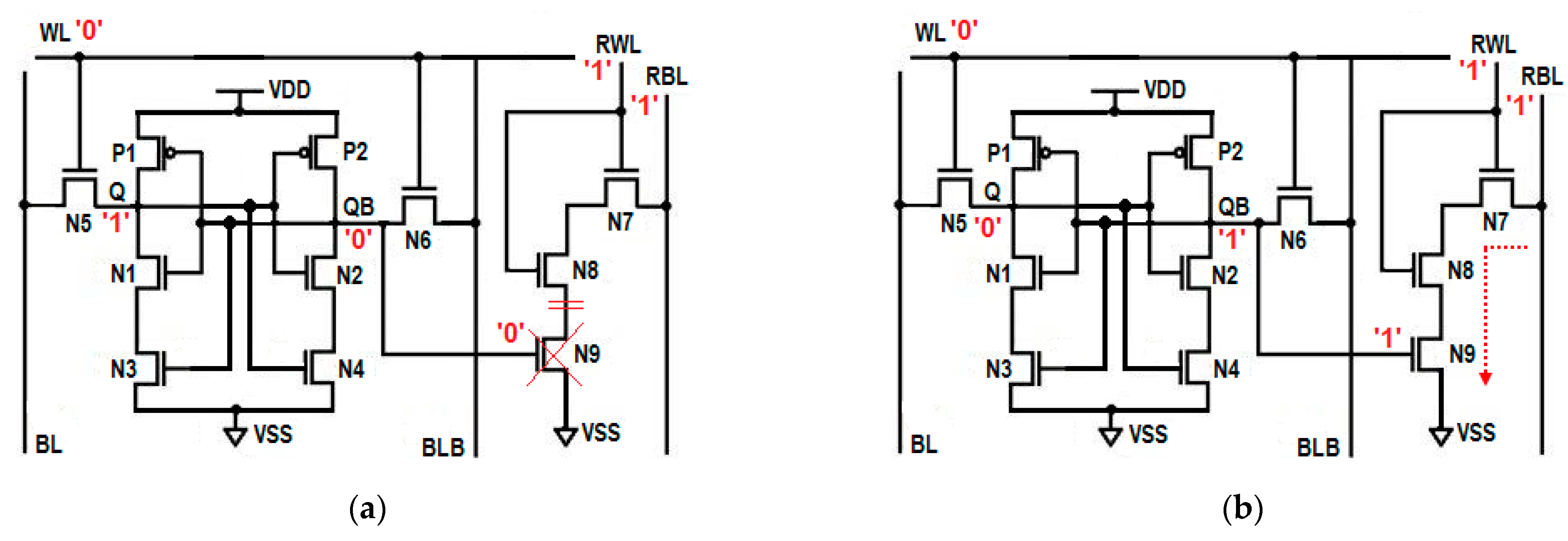
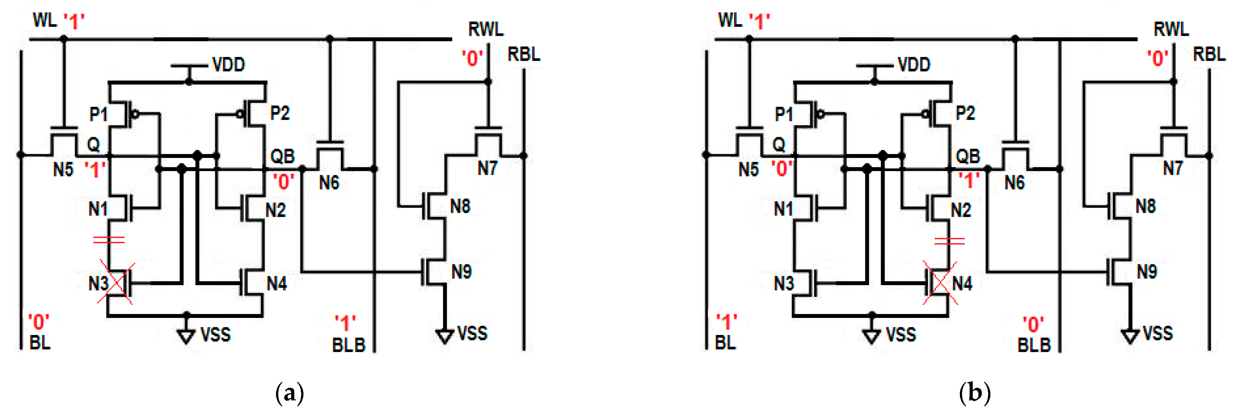
3.3.2. Write Operation
3.3.3. Hold Operation
4. Results and Discussions
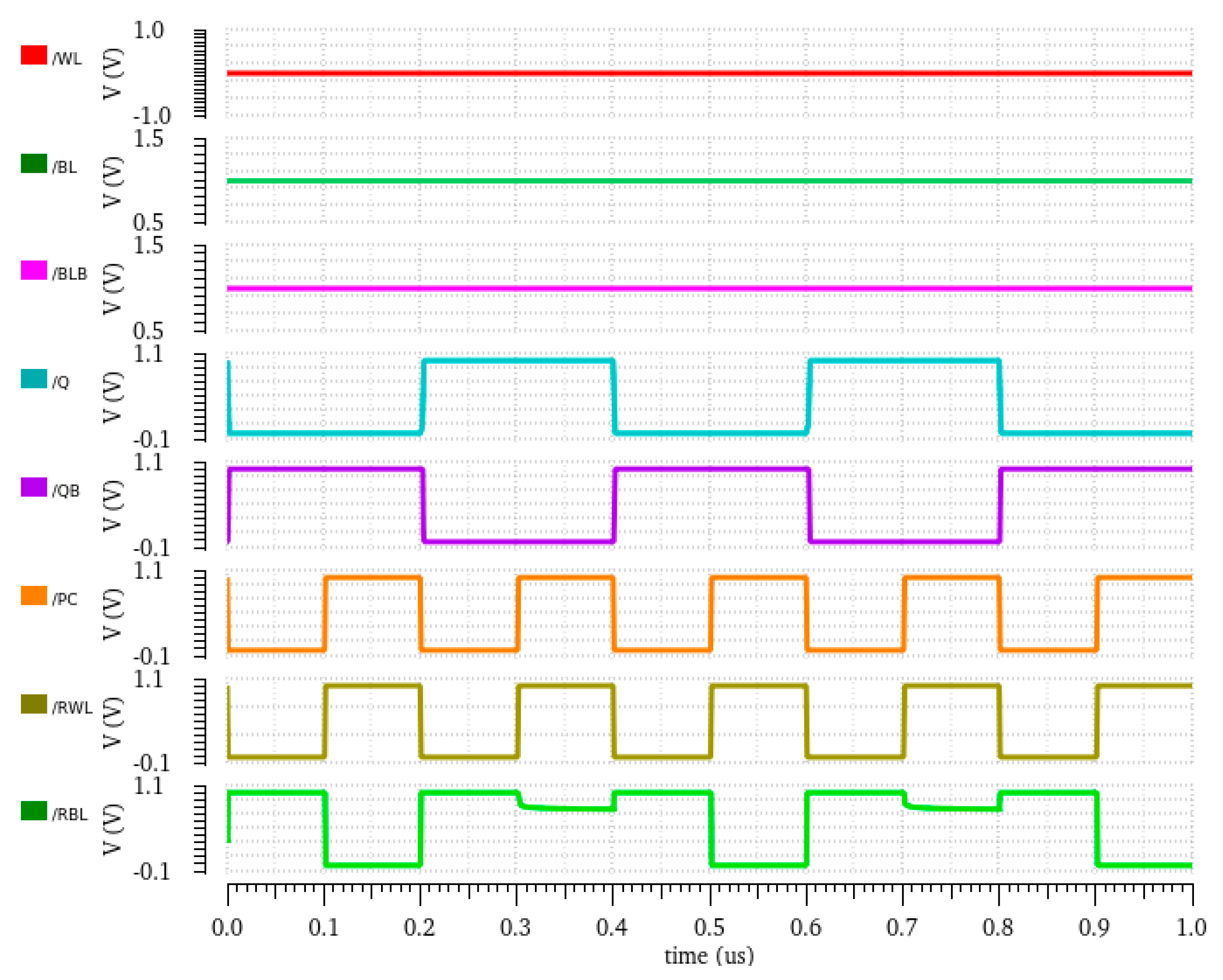
4.1. Simulation Environment
4.2. PVT Variation Analysis
- Process Variation
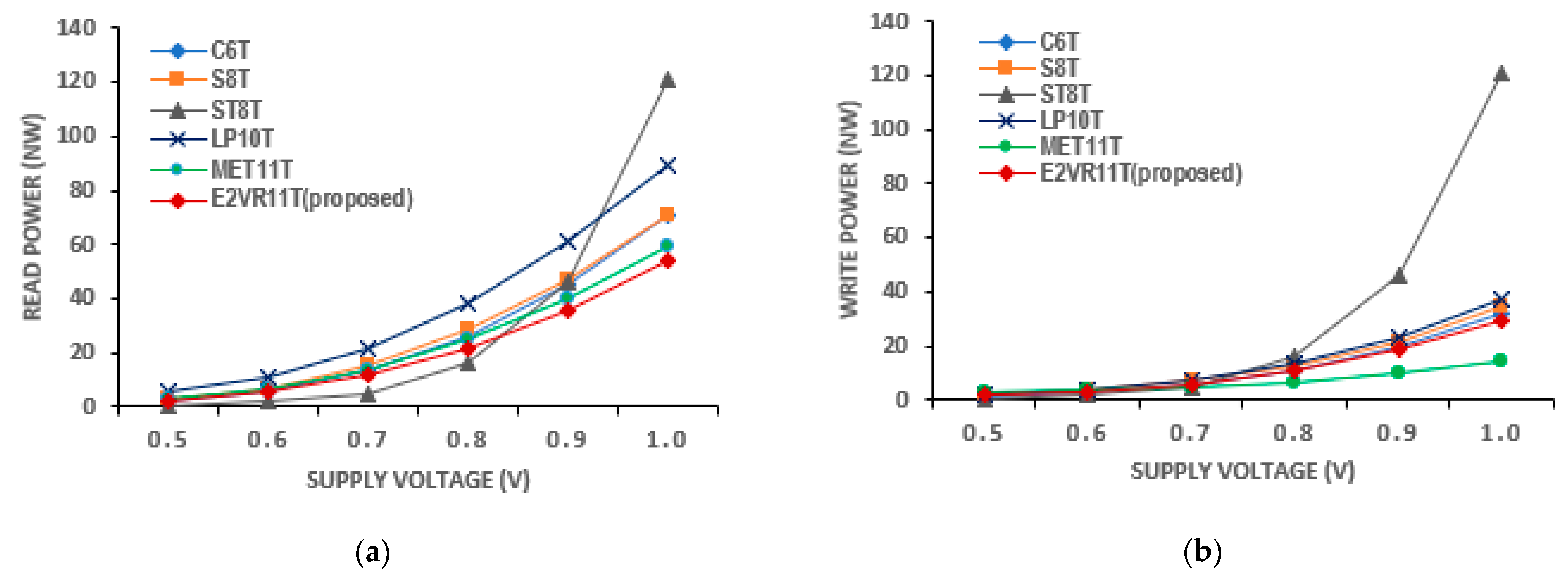
- Voltage Variation
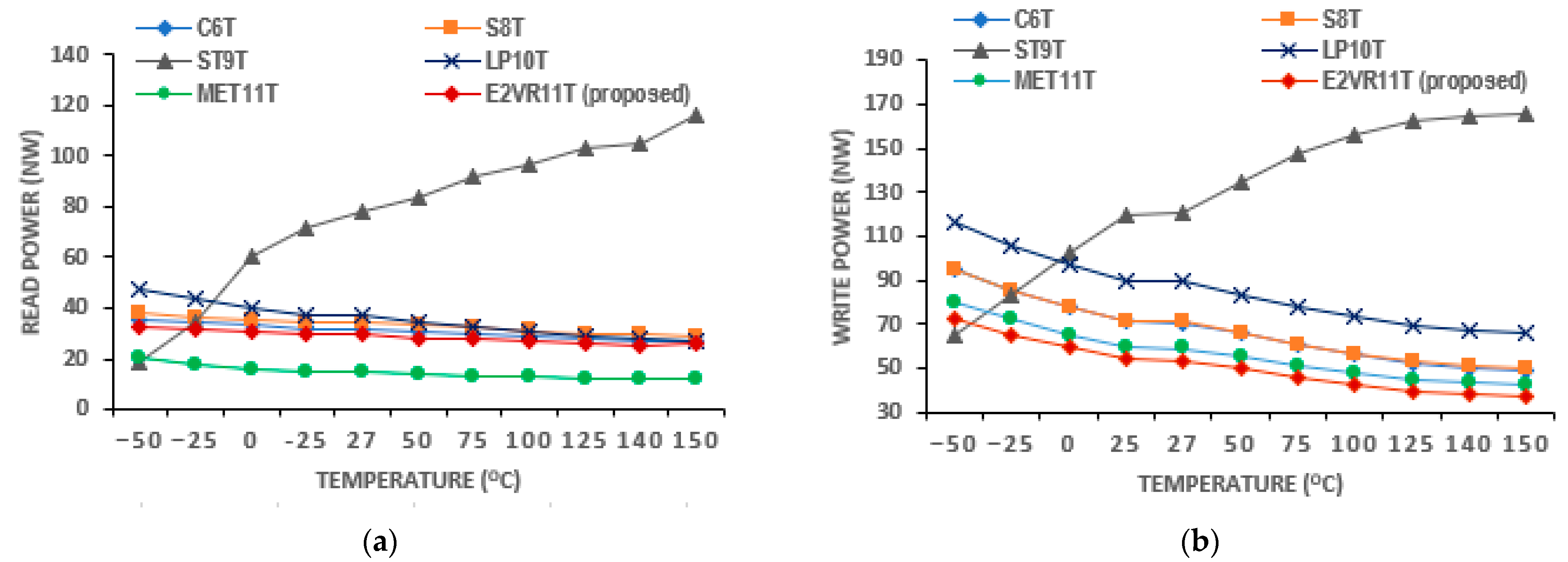
- Temperature Variation
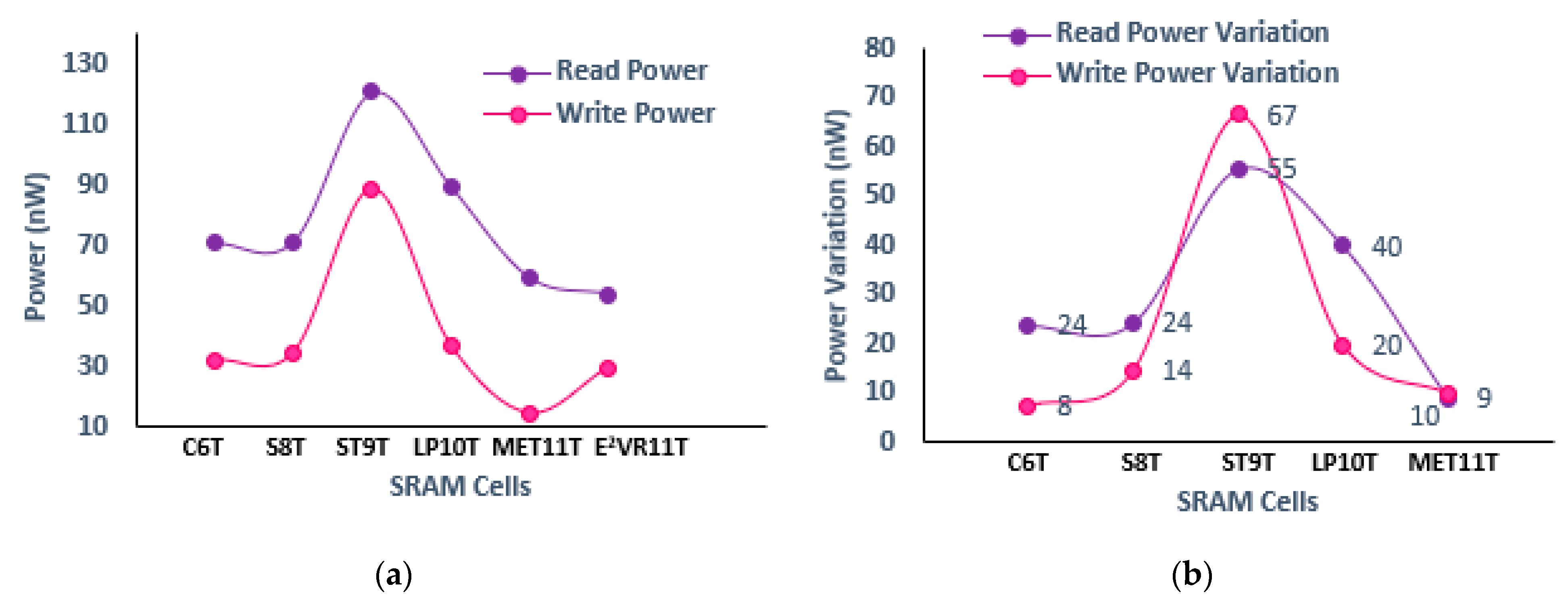
4.3. E2VR11T SRAM Power Consumption
4.3.1. Dynamic Power Consumption
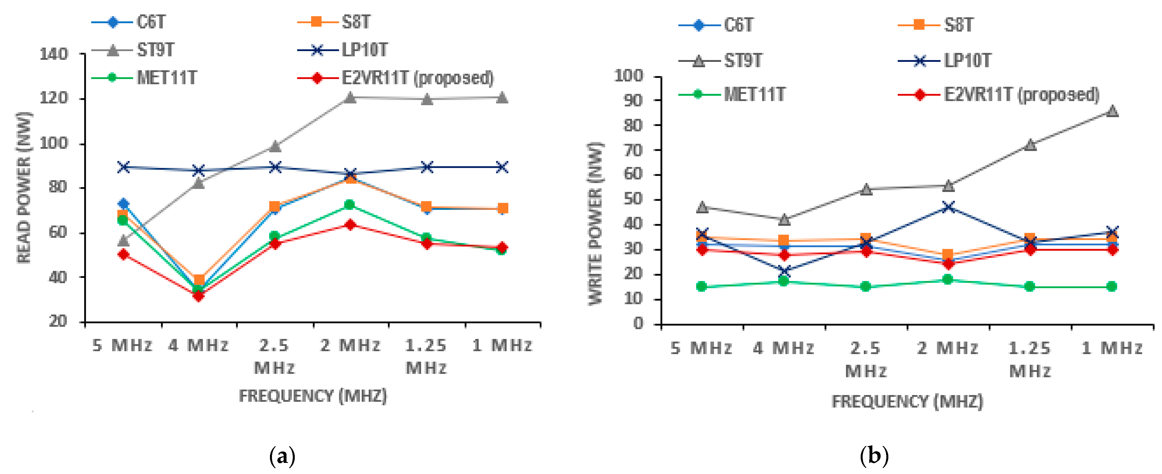
4.3.2. Read and Write Power Consumption
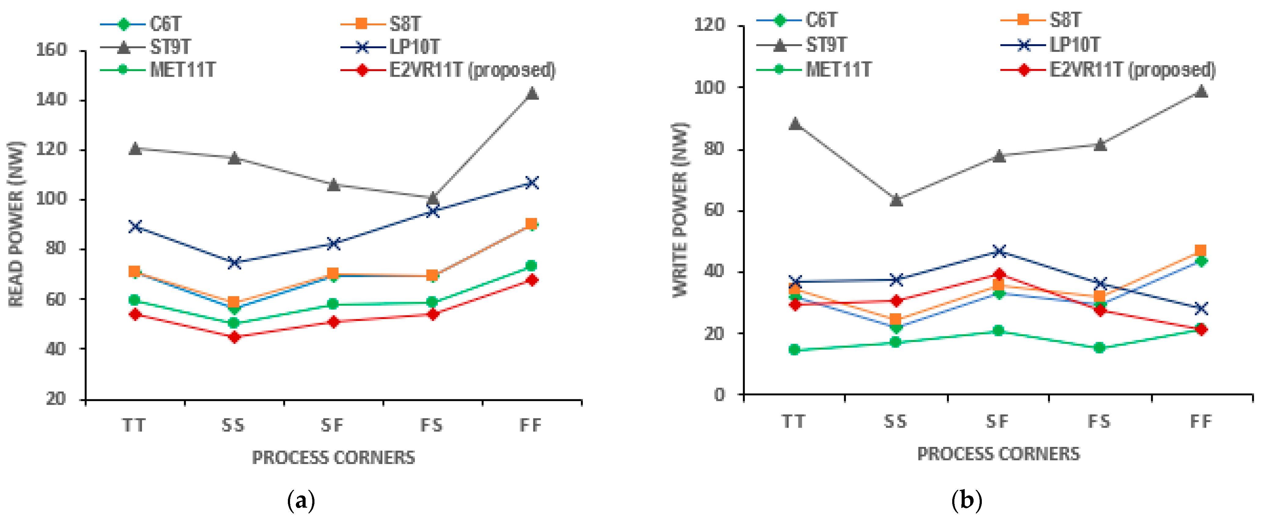
4.3.3. PVT Variation of Read and Write Power Analysis
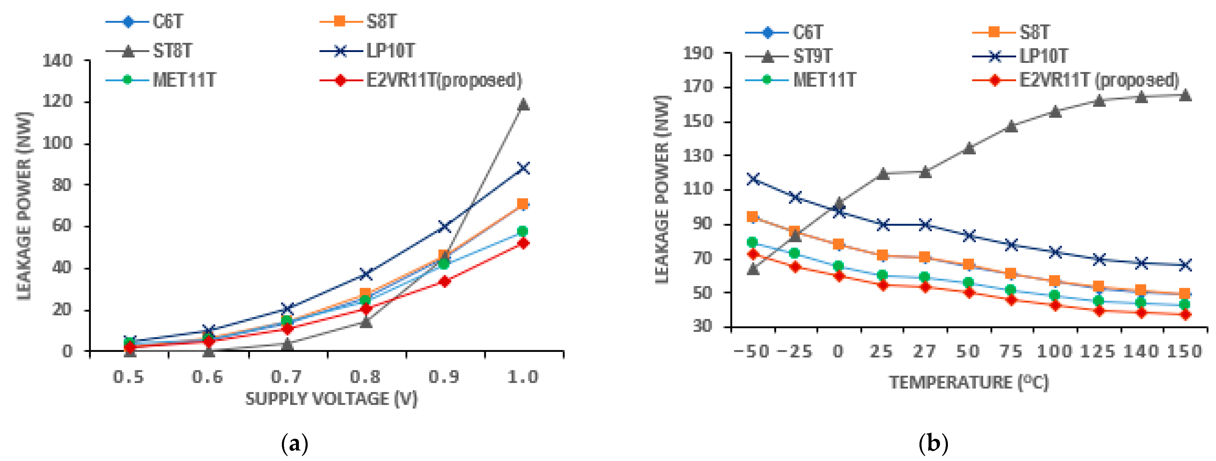
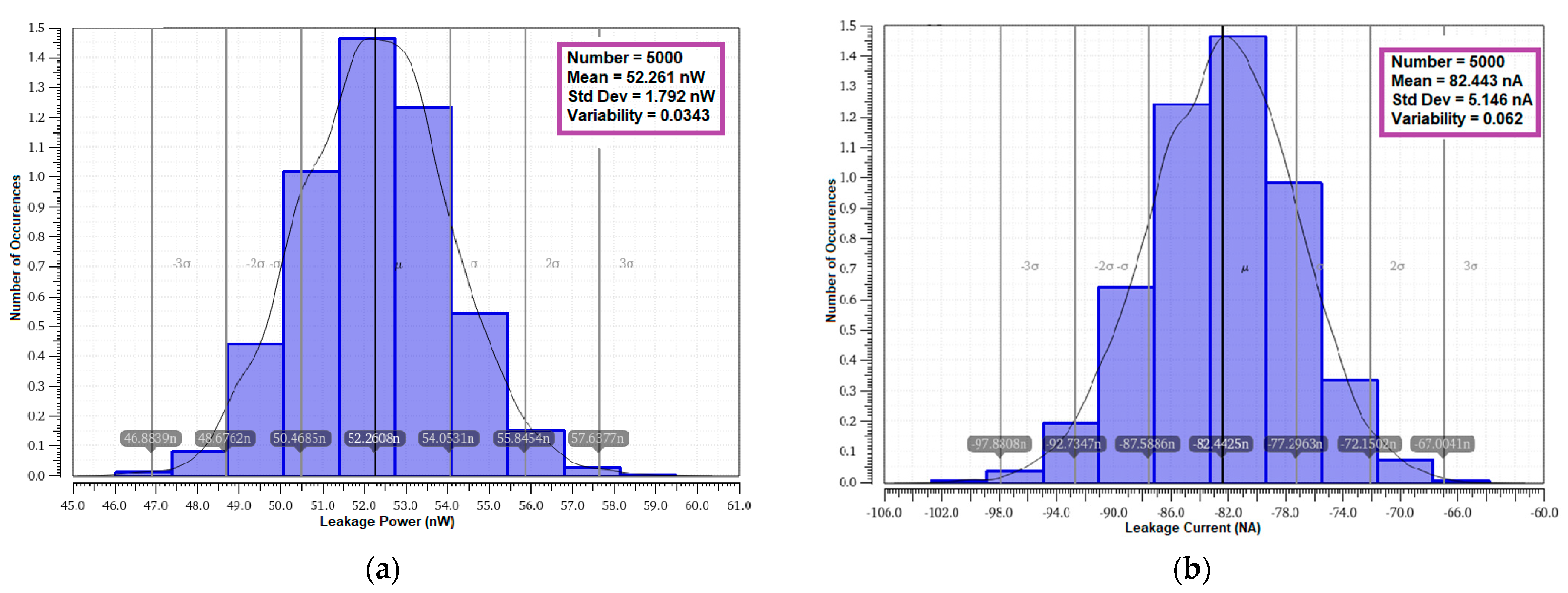
4.3.4. Leakage Power Consumption
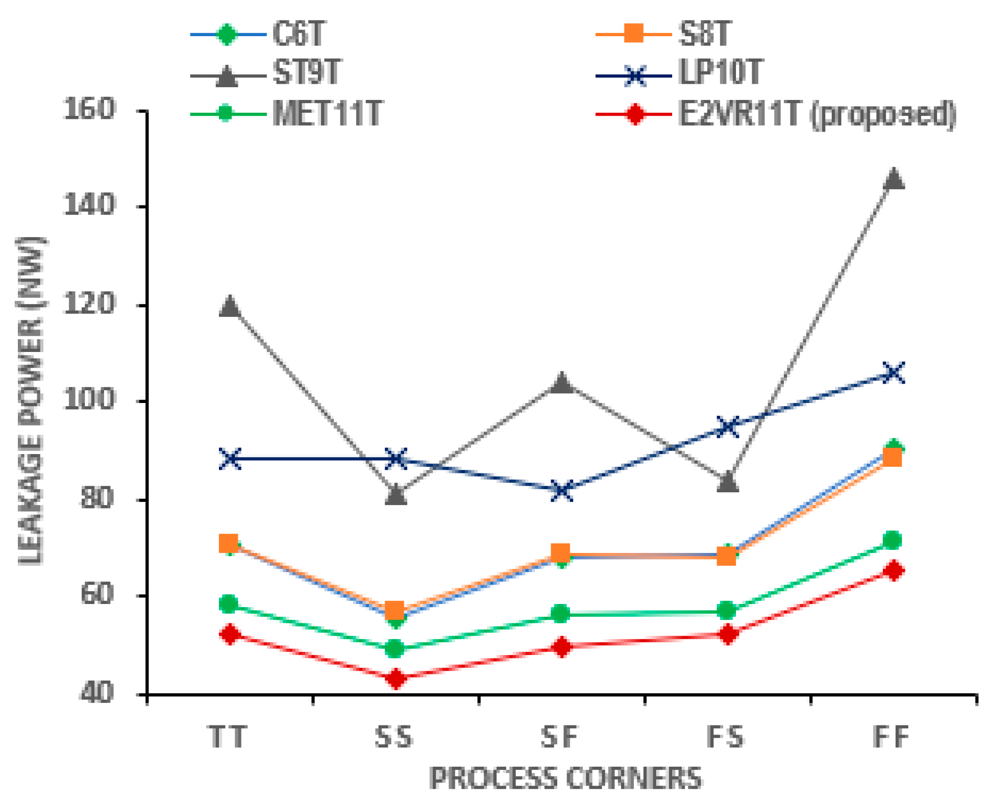
4.3.5. PVT Variation of Leakage Power Analysis
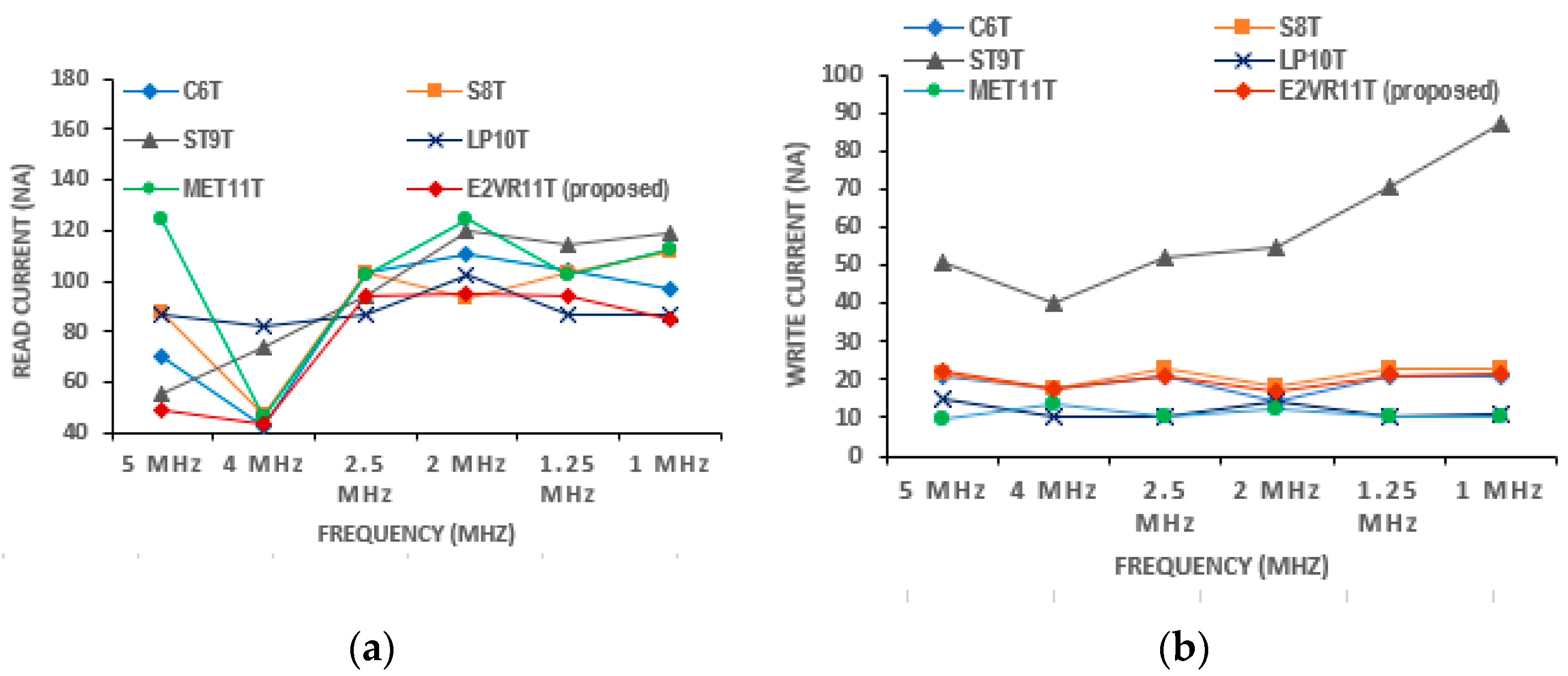
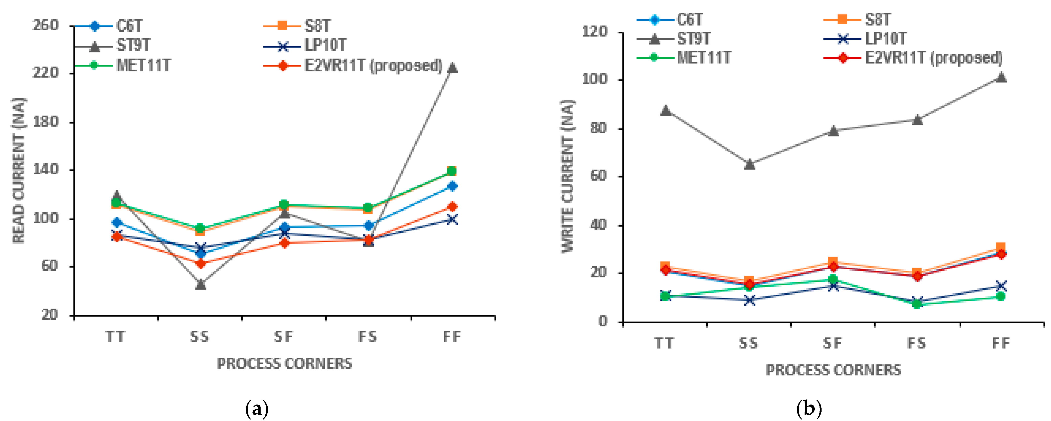
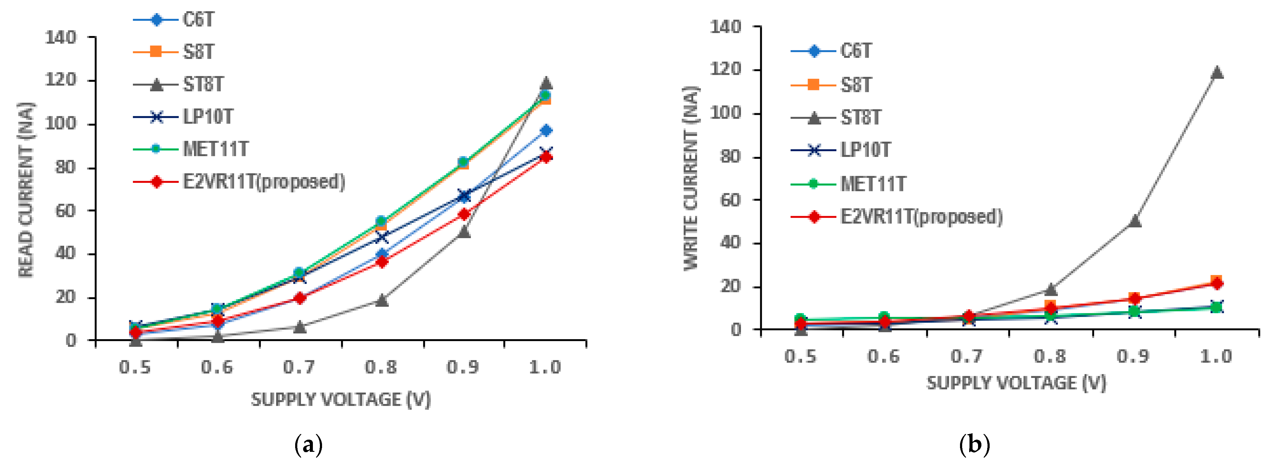
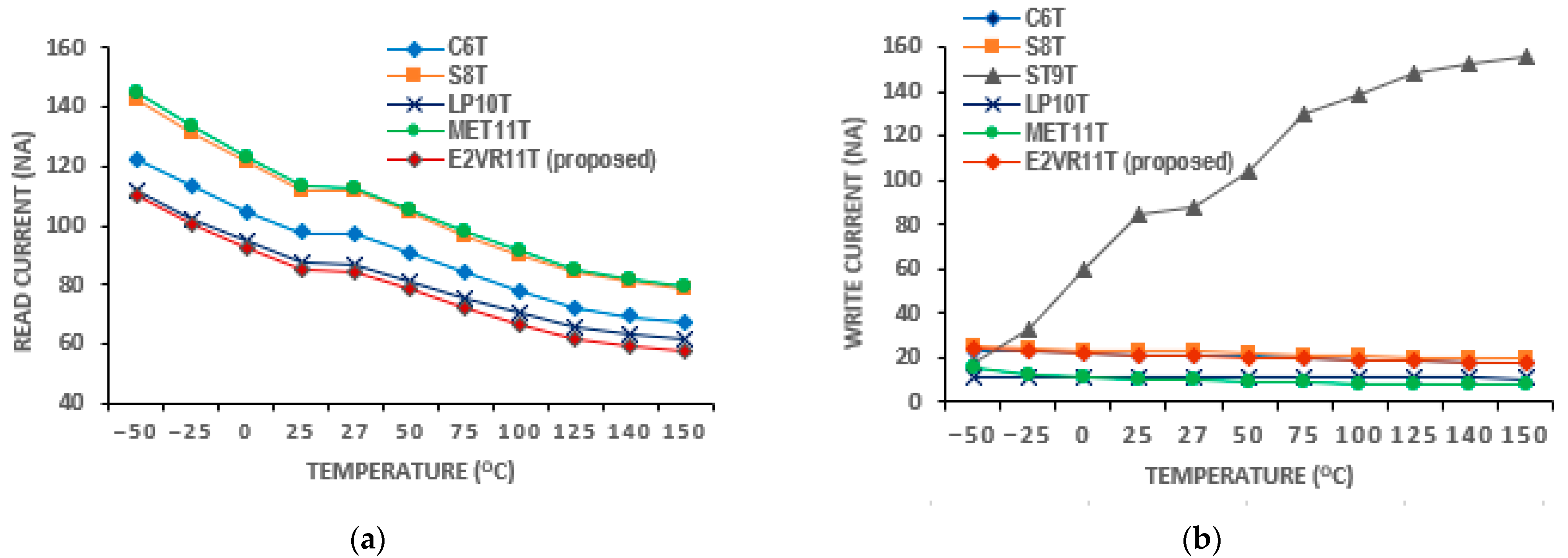
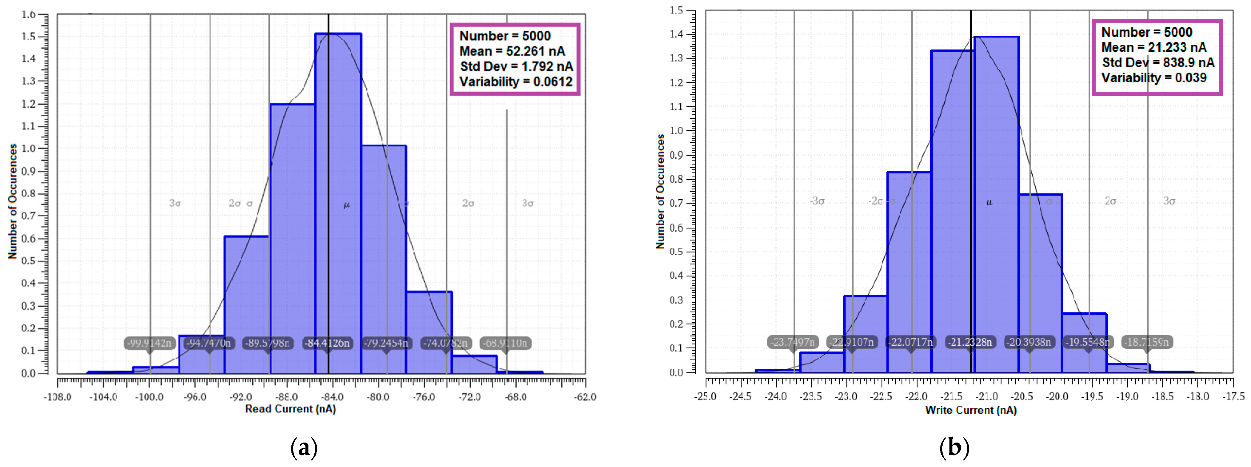
4.4. E2VR11T SRAM Current
PVT Variation of Current Analysis
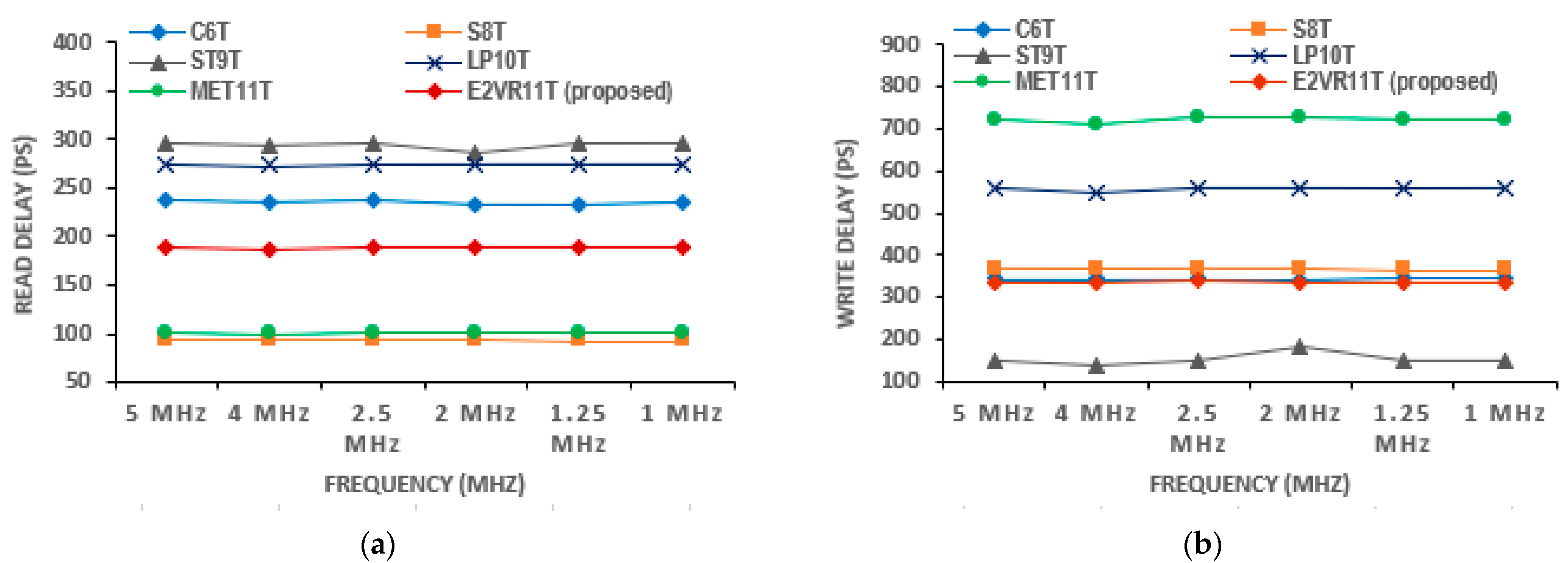
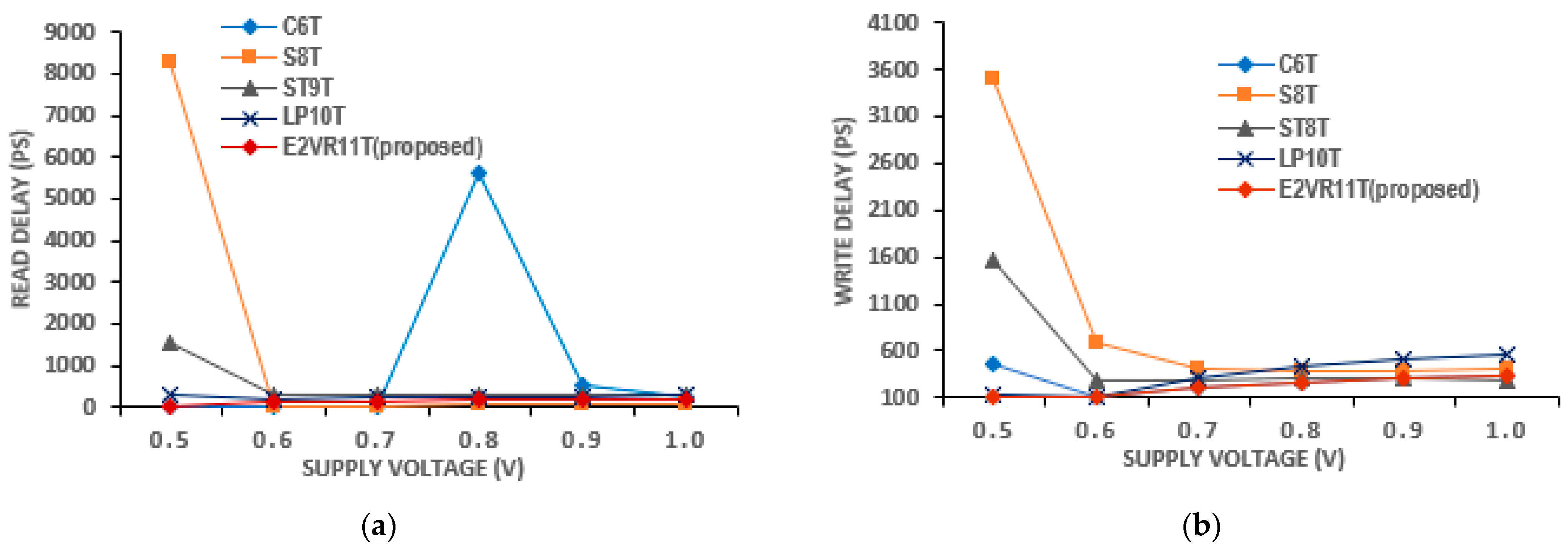
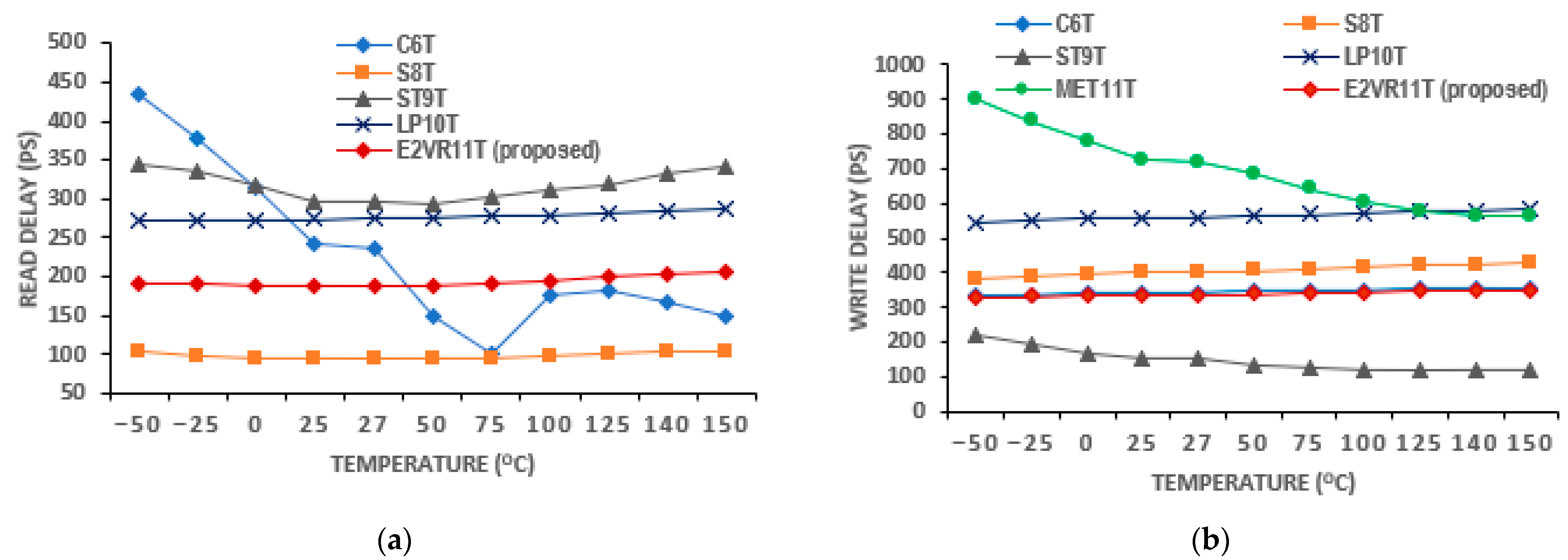
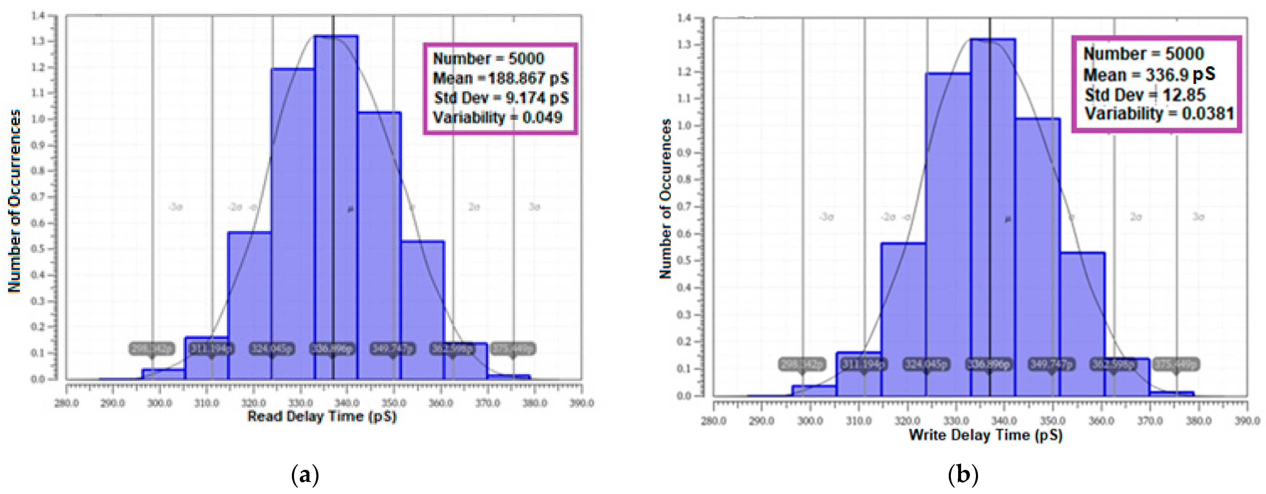
4.5. E2VR11T SRAM Delay Time
4.5.1. Read Delay Time (RDT)and Write Delay Time (WDT)
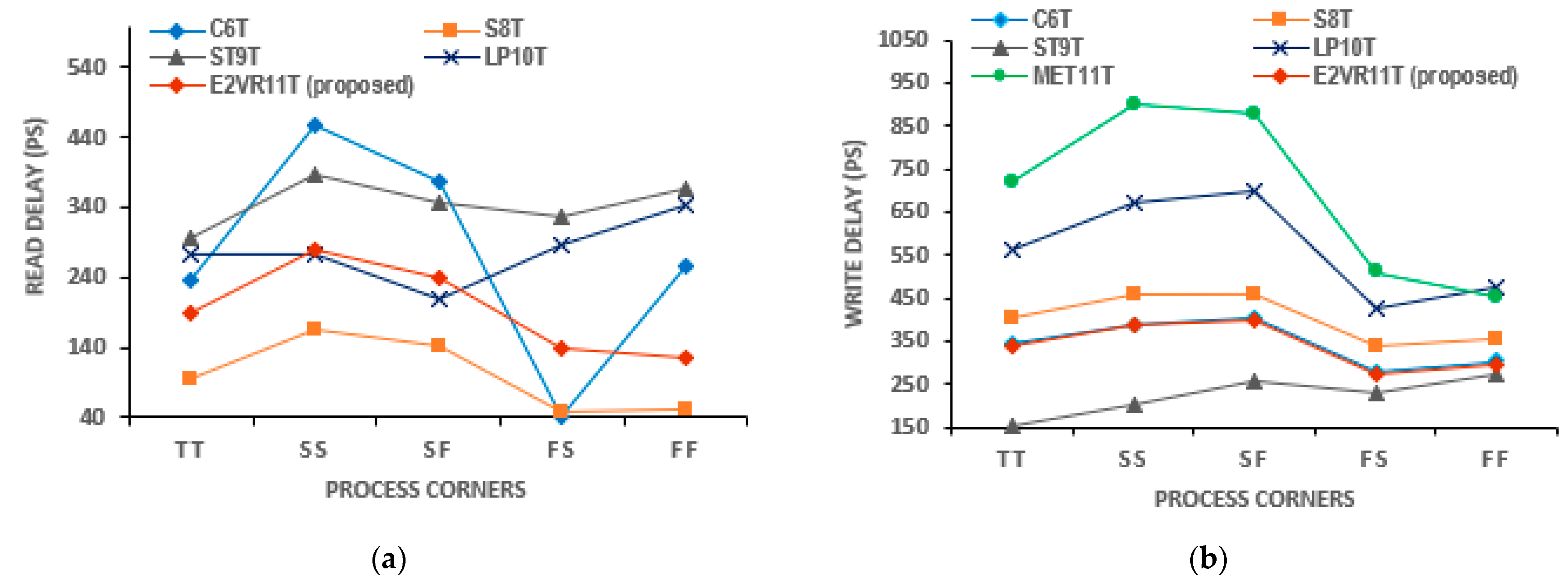
4.5.2. PVT Variation of Delay Time Analysis
4.6. E2VR11T SRAM Energy Consumption
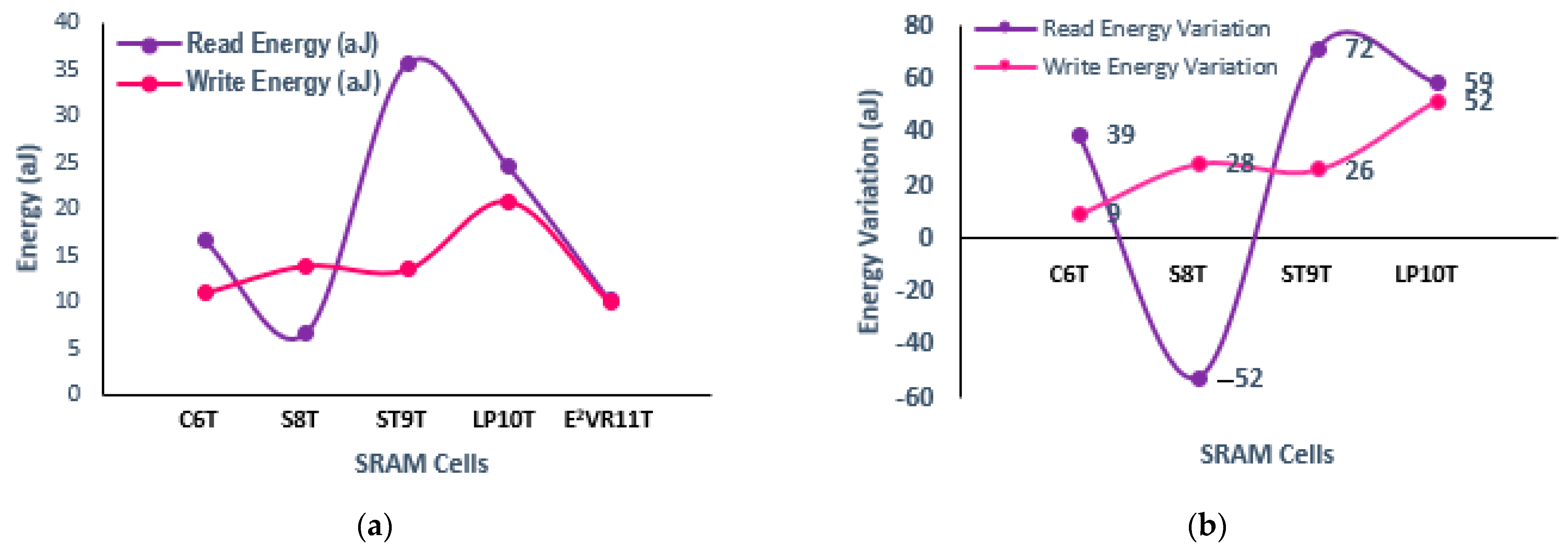
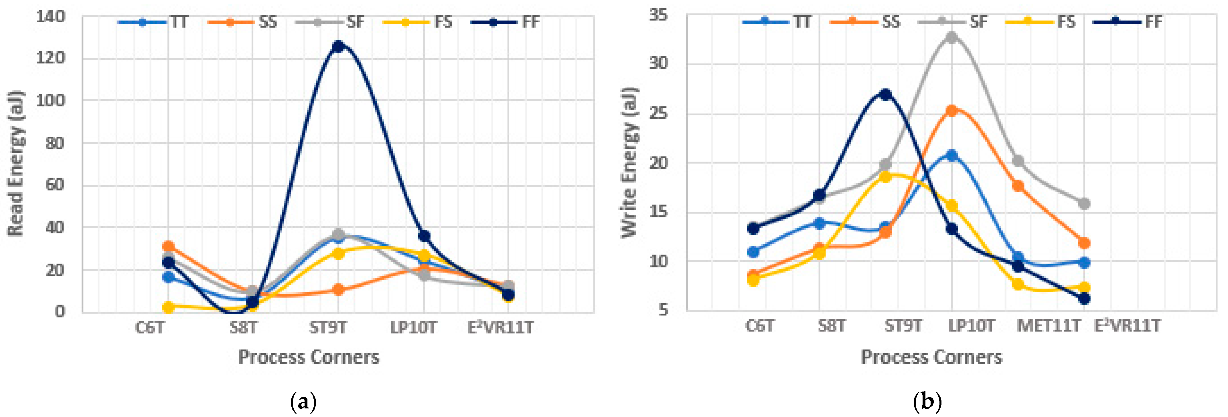
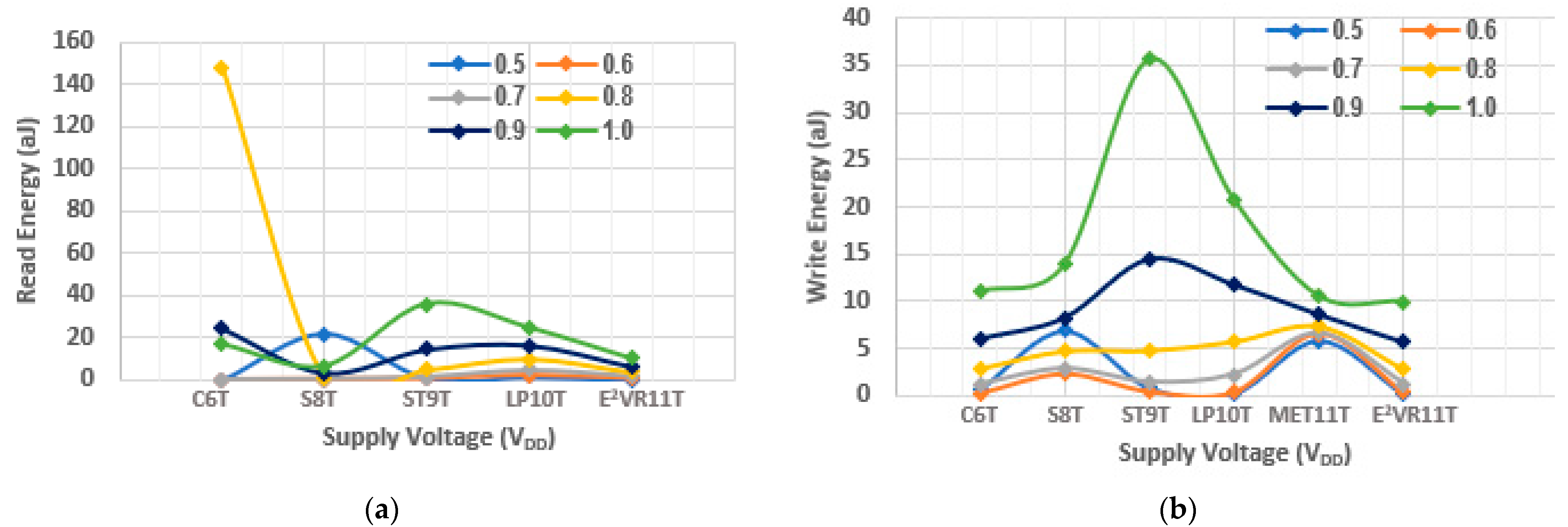
4.6.1. Read and Write Energy
4.6.2. PVT Variation of Energy Analysis
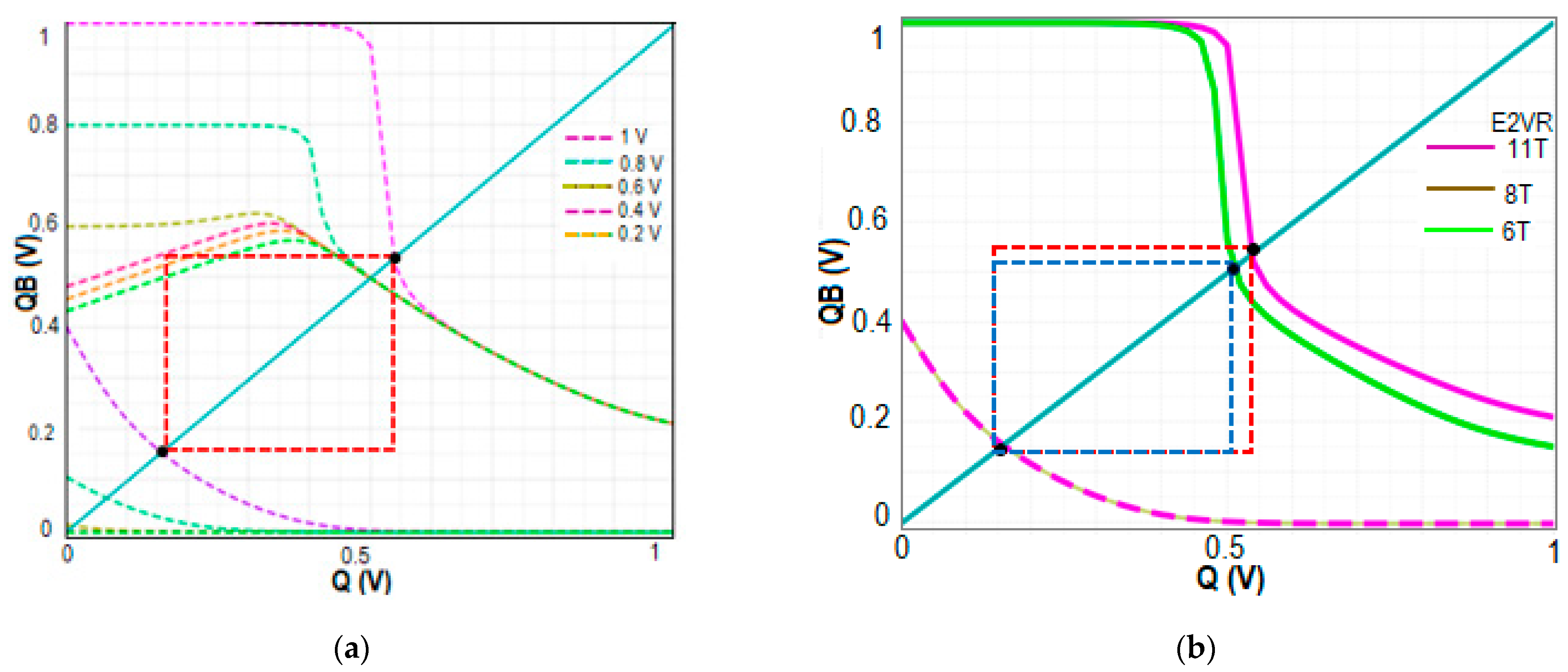
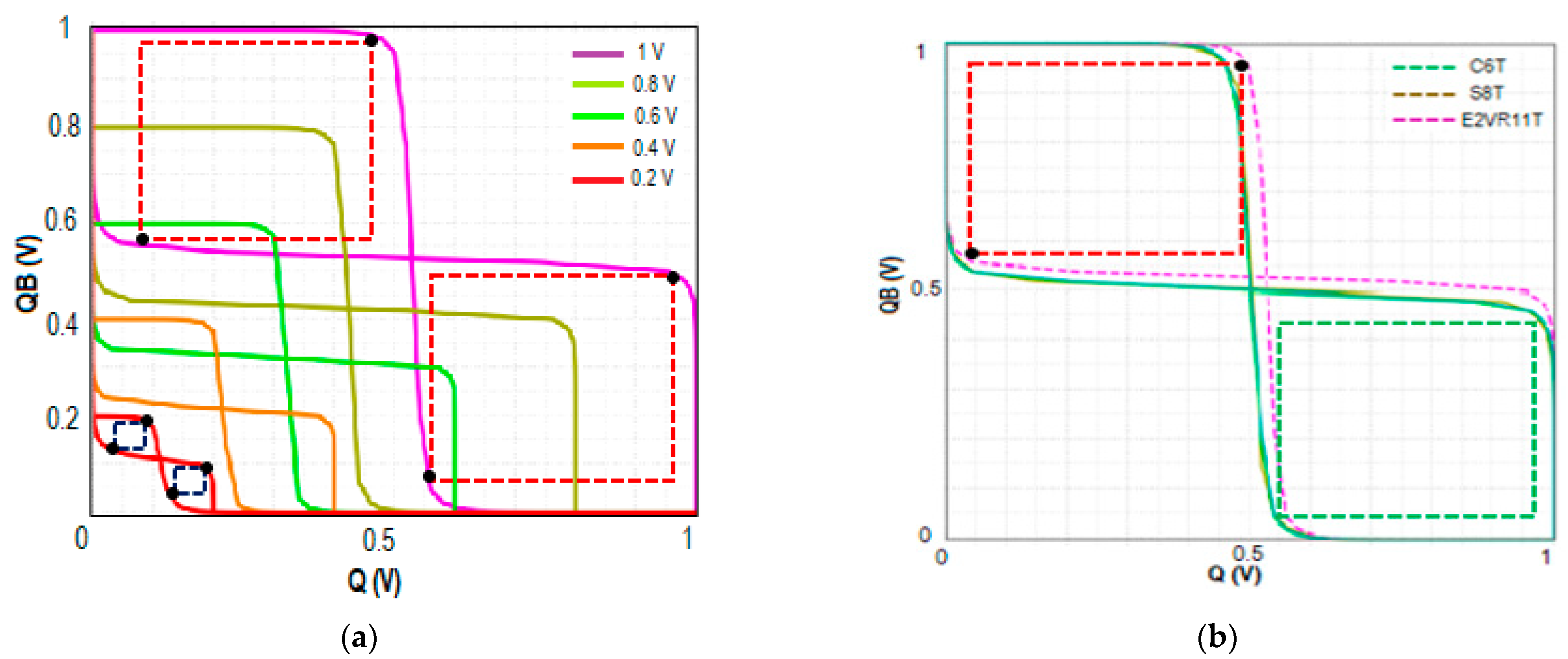
4.7. E2VR11T SRAM Stability
4.7.1. Read Stability
4.7.2. Write Stability
4.7.3. Hold Static Noise Margin (HSNM)
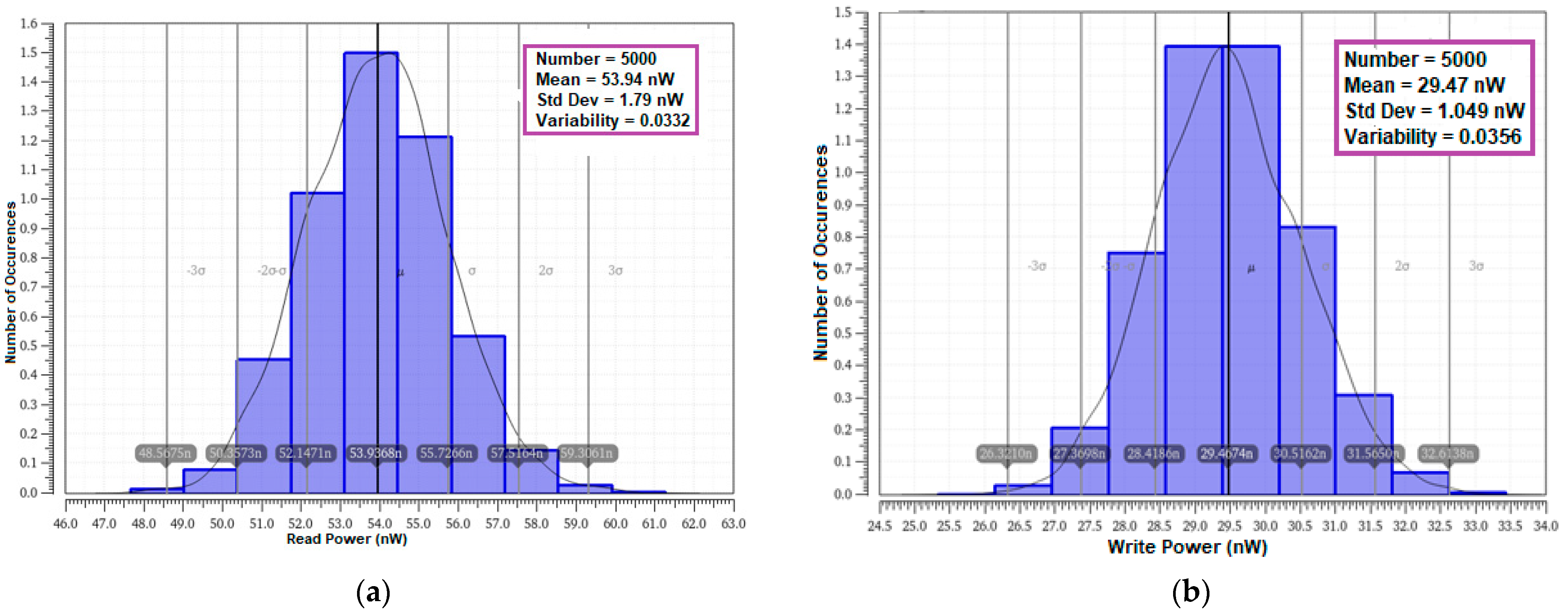
4.8. E2VR11T SRAM Variability Investigation
4.8.1. Power Variability
4.8.2. Leakage Power and Leakage Current Variability
4.8.3. Current Variability
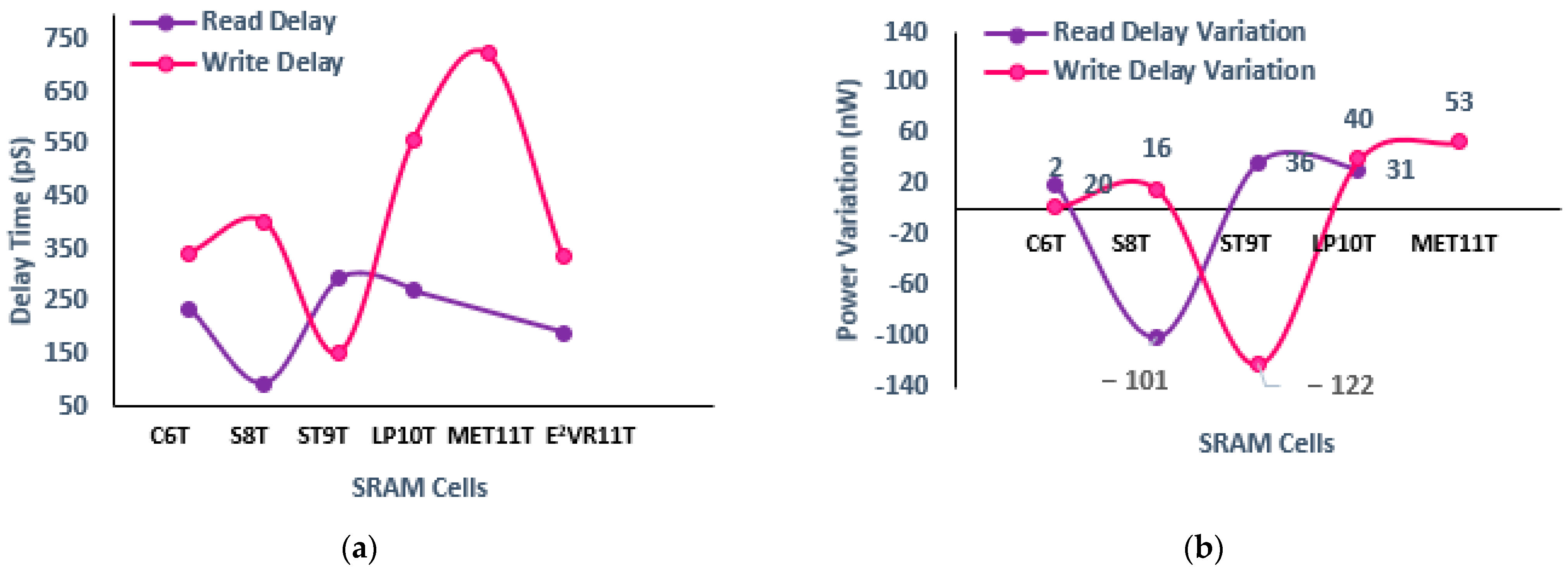
4.8.4. Delay Time Variability
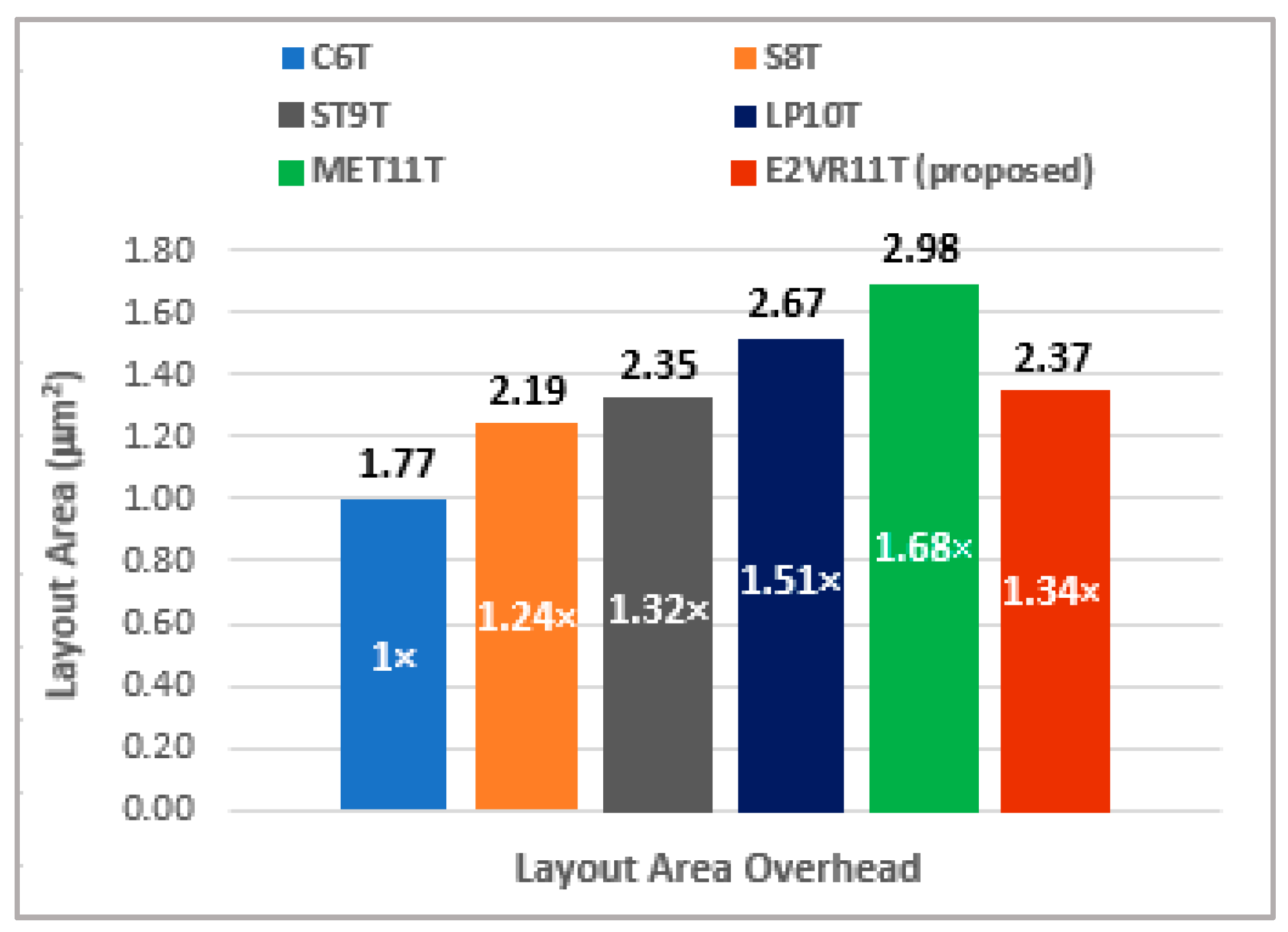
4.9. E2VR11T SRAM Layout Area Considerations
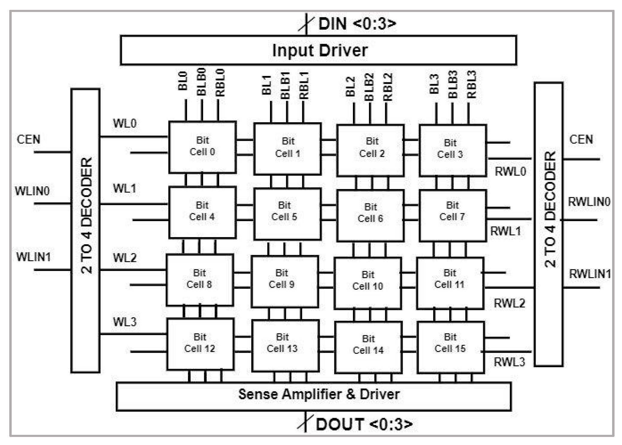
4.10. E2VR11T SRAM Memory Array
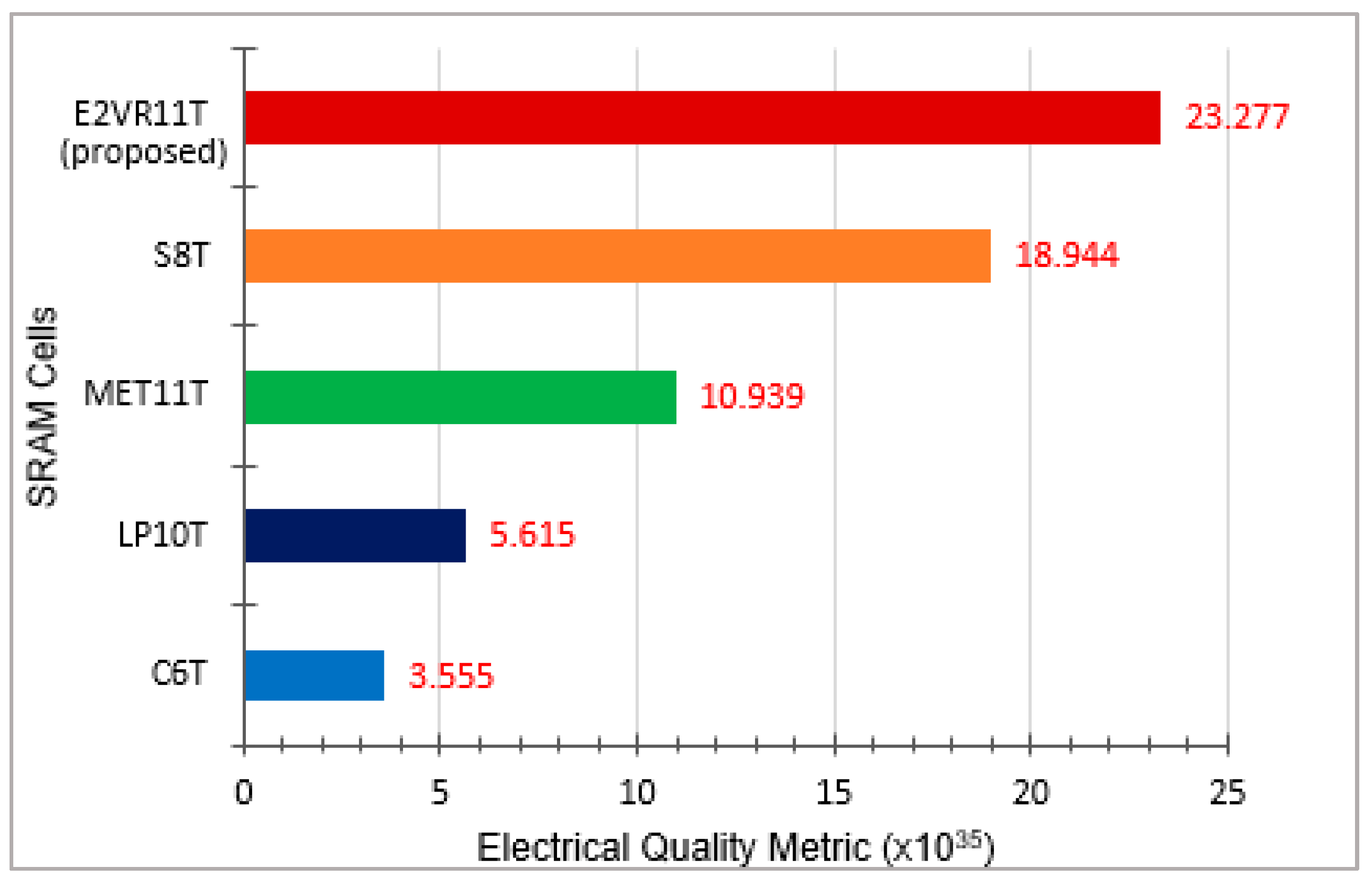
4.11. E2VR11T SRAM Electrical Quality Metric (EQM)
4.12. E2VR11T SRAM Overall Performance
5. Conclusions
Author Contributions
Funding
Institutional Review Board Statement
Informed Consent Statement
Data Availability Statement
Acknowledgments
Conflicts of Interest
References
- Perera, C.; Liu, C.H.; Jayawardena, S.; Chen, M. A Survey on Internet of Things from Industrial Market Perspective. IEEE Access 2014, 2, 1660–1679. [Google Scholar] [CrossRef]
- Hiramoto, T.; Takeuchi, K.; Mizutani, T.; Ueda, A.; Saraya, T.; Kobayashi, M.; Yamamoto, Y.; Makiyama, H.; Yamashita, T.; Oda, H.; et al. Ultra-low power and ultra-low voltage devices and circuits for IoT applications. In Proceedings of the 2016 IEEE Silicon Nanoelectronics Workshop (SNW), Honolulu, HI, USA, 12–13 June 2016; pp. 9.1–9.2. [Google Scholar] [CrossRef]
- Hodge, V.J.; O’Keefe, S.; Weeks, M.; Moulds, A. Wireless sensor networks for condition monitoring in the railway industry: A survey. IEEE Trans. Intell. Transp. Syst. 2015, 16, 1088–1106. [Google Scholar] [CrossRef]
- Teodor, C.; Michael, N.; Raoul, V. Upset hardened memory design for submicron cmos technology. IEEE Trans. Nucl. Sci. 1996, 43, 2874–2878. [Google Scholar] [CrossRef]
- Singh, P.; Reniwal, B.S.; Vijayvargiya, V.; Sharma, V.; Vishvakarma, S.K. Ultra low power-high stability, positive feedback controlled (PFC) 10T SRAM cell for look up table (LUT) design. Integration 2018, 62, 1–13. [Google Scholar] [CrossRef]
- Agrawal, K.; Nassif, S. The Impact of Random Device Variation on SRAM Cell Stability in Sub-90-nm CMOS Technologies. IEEE Trans. Very Large Scale Integr. (VLSI) Syst. 2008, 16, 86–97. [Google Scholar] [CrossRef]
- Chang, Y.J.; Lai, F.; Yang, C.L. Zero-Aware Asymmetric SRAM Cell for reducing Cache Power in Writing Zero. IEEE Trans. Very Large Scale Integr. (VLSI) Syst. 2004, 12, 827–836. [Google Scholar] [CrossRef]
- Vibhu, S.; Francky, C.; Wil, D. Introduction. In SRAM Design for Wireless Sensor Networks Energy Efficient and Variability Resilient Techniques; Ismail, M., Sawan, M., Eds.; Springer Science & Business Media: Heidelberg, Germany; Dordrecht, The Netherlands; London, UK, 2013; Volume 1, pp. 1–8. [Google Scholar]
- Chen, H.; Jun, Y.; Meng, Z.; Xiulong, W. A 12 T subthreshold SRAM Bit-cell for Medical Device Application. In Proceedings of the International Cyber-Enabled Distributed Computing and Knowledge Discovery Conference, Beijing, China, 10–12 October 2011; pp. 540–543. [Google Scholar] [CrossRef]
- Ahmad, S.; Gupta, M.K.; Alam, N.; Hasan, M. Low leakage single bitline 9T (SB9T) static random access memory. Microelectron. J. 2017, 6, 1–11. [Google Scholar] [CrossRef]
- Sharma, V.; Bisht, P.; Dalal, A.; Gopal, M.; Vishvakarma, S.K. Half-select free bit-line sharing 12 T SRAM with double-adjacent bits soft error correction and a reconfigurable FPGA for low-power applications. Int. J. Electron. Commun. 2019, 104, 10–22. [Google Scholar] [CrossRef]
- Kim, T.H.; Jeong, H.; Park, J.; Kim, H.; Song, T. An Embedded Level-Shifting Dual-Rail SRAM for High-Speed and Low-Power Cache. IEEE Access 2020, 8, 187126–187139. [Google Scholar] [CrossRef]
- Pal, S.; Islam, A. 9-T SRAM cell for reliable ultralow-power applications and solving multibit soft-error issue. IEEE Trans. Device Mater. Reliab. 2016, 16, 172–182. [Google Scholar] [CrossRef]
- Pal, S.; Bose, S.; Ki, W.H.; Islam, A. Characterization of half-select free write assist 9 T SRAM cell. IEEE Trans. Electron Devices 2019, 66, 4745–4752. [Google Scholar] [CrossRef]
- Lorenzo, R.; Pailly, R. Single bit-line 11T SRAM cell for low power and improved stability. IET Comput. Digit. Tech. 2020, 14, 114–121. [Google Scholar] [CrossRef]
- Zhiting, L.; Zhiyong, Z.; Honglan, Z.; Chunyu, P.; Xiulong, W.; Yuan, Y.; Jianchao, N.; Junning, C. Two-Direction In-Memory Computing Based on 10T SRAM With Horizontal and Vertical Decoupled Read Ports. IEEE J. Solid-State Circuits 2021, 56, 2832–2844. [Google Scholar] [CrossRef]
- Yang, H.; Hu, J.; Zhu, H. Novel SRAM cells using dual-threshold independent gate FinFETs. In Proceedings of the IEEE 17th International Conference on Nanotechnology (IEEE-NANO), Pittsburgh, PA, USA, 4–8 July 2017; pp. 358–359. [Google Scholar] [CrossRef]
- Sharma, V.; Gopal, M.; Singh, P.; Vishvakarma, S.K.; Chouhan, S.S. A robust, ultra-low-power, data-dependent power supplied 11T SRAM cell with expanded read/write stabilities for internet-of-things applications. Analog Integr. Circuits Signal Process. 2019, 98, 331–346. [Google Scholar] [CrossRef]
- Grace, P.S.; Sivamangai, N.M. Design of 10T SRAM Cell for High SNM and Low Power. In Proceedings of the Third International Conference on Devices, Circuits and Systems (ICDCS’16), Coimbatore, India, 3–5 March 2016; pp. 281–285. [Google Scholar] [CrossRef]
- Arandilla, C.D.C.; Alvarez, A.B.; Roque, C.R.K. Static Noise Margin of 6T SRAM Cell in 90-nm CMOS. In Proceedings of the 2011 UkSim 13th International Conference on Computer Modelling and Simulation, Cambridge, UK, 30 March–1 April 2011; pp. 534–539. [Google Scholar] [CrossRef]
- Noguchi, H.; Okumura, S.; Iguchi, Y.; Fujiwara, H.; Morita, Y. Which is the best dual-port SRAM in 45-nm process technology-8T, 10T single end, and 10T differential. In Proceedings of the IEEE International Conference on Integrated Circuit Design and Technology, (IEEE ICICDT), Grenoble, France, 2–4 June 2008; pp. 55–58. [Google Scholar] [CrossRef]
- Keonhee, C.; Juhyun, P.; Tae, W.O.; Seong, O.J. One-Sided Schmitt-Trigger-Based 9T SRAM Cell for Near-Threshold Operation. IEEE Trans. Circuits Syst. I Regul. Pap. 2020, 67, 1551–1561. [Google Scholar] [CrossRef]
- Erfan, A.; Farzaneh, I.; Morteza, G. A Reliable Low Standby Power 10T SRAM Cell With Expanded Static Noise Margins. IEEE Trans. Circuits Syst. I Regul. Pap. 2022, 69, 1606–1616. [Google Scholar] [CrossRef]
- Sharma, V.; Gupta, N.; Shah, A.P.; Vishvakarma, S.K.; Chouhan, S.S. A reliable, multi-bit error tolerant 11T SRAM memory design for wireless sensor nodes. Analog Integr. Circuits 2021, 107, 339–352. [Google Scholar] [CrossRef]
- Grossar, E.; Stucchi, M.; Maex, K.; Dehaene, W. Read Stability and Write-Ability Analysis of SRAM Cells for Nanometer Technologies. IEEE J. Solid-State Circuits 2006, 41, 2577–2588. [Google Scholar] [CrossRef]
- Gierczynski, N.; Borot, B.; Planes, N.; Brut, H. A new combined methodology for write margin extraction of advanced SRAM. In Proceedings of the 2007 IEEE International Conference on Microelectronic Test Structures, Bunkyo-ku, Japan, 19–22 March 2007; pp. 97–100. [Google Scholar] [CrossRef]
- Naghizadeh, S.; Gholami, M. Two Novel Ultra-Low-Power SRAM Cells with Separate Read and Write Path. Circuits Syst. Signal Process. 2019, 38, 287–303. [Google Scholar] [CrossRef]
- Gupta, S.; Gupta, K.; Pandey, N. A 32-nm Subthreshold 7T SRAM bit cell with Read Assist. IEEE Trans. Very Large Scale Integr. (VLSI) Syst. 2017, 25, 3473–3483. [Google Scholar] [CrossRef]
- Sargunam, T.G.; Soong, L.W.; Prabhu, C.M.R.; Ajay, K.S. Process Tolerant and Power Efficient SRAM Cell for Internet of Things Applications. Comput. Mater. Contin. 2022, 72, 3425–3446. [Google Scholar] [CrossRef]
- Ajay, K.S.; Mohammadsadegh, S.; Venkataseshaiah, C. Design of single-ended energy efficient data-dependent-write-assist dynamic (DDWAD) SRAM cell for improved stability and reliability. Analog Integr. Circuits Signal Process. 2017, 90, 411–426. [Google Scholar] [CrossRef]
- Singh, P.; Vishvakarma, S.K. Ultra-Low Power, Process-Tolerant 10 T (PT10T) SRAM with Improved Read/Write Ability for Internet of Things (IoT) Applications. J. Low Power Electron. Appl. 2017, 7, 24. [Google Scholar] [CrossRef]
- Islam, A.; Hasan, M. A technique to mitigate impact of process, voltage and temperature variations on design metrics of SRAM cell. Microelectron. Reliab. 2012, 52, 405–411. [Google Scholar] [CrossRef]
- Gupta, N.; Shah, A.P.; Khan, S.; Vishvakarma, S.K.; Waltl, M.; Girard, P. Error-Tolerant Reconfigurable VDD 10T SRAM Architecture for IoT Applications. Electronics 2021, 10, 1718. [Google Scholar] [CrossRef]
- Sachdeva, A.; Tomar, V.K. Design of Low Power Half Select Free 10T Static Random-Access Memory Cell. J. Circuits Syst. Comput. 2021, 30, 2150073. [Google Scholar] [CrossRef]
- Sanvale, P.; Gupta, N.; Neema, V.; Shah, A.P.; Vishvakarma, S.K. An improved read-assist energy on efficient single ended P-P-N based 10 T SRAM cell for wireless sensor network. Microelectron. J. 2019, 92, 104611. [Google Scholar] [CrossRef]
- Pal, S.; Islam, A. Variation tolerant differential 8 T SRAM cell for ultralow power applications. IEEE Trans. Comput.-Aided Des. Integr. Circuits Syst. 2015, 35, 549–558. [Google Scholar] [CrossRef]
- Duari, C.; Birla, S. Low Leakage SRAM Cell with Improved Stability for IoT Applications. Procedia Comput. Sci. 2020, 171, 1469–1478. [Google Scholar] [CrossRef]
- Takeda, K.; Ikeda, H.; Hagihara, Y.; Nomura, M.; Kobatake, H. Redefinition of write margin for next-generation SRAM and write-margin monitoring circuit. In Proceedings of the 2006 IEEE International Solid-State Circuits Conference-Digest of Technical Papers, San Francisco, CA, USA, 6–9 February 2006; pp. 2602–2611. [Google Scholar] [CrossRef]
- Elangovan, M.; Erfan, A.; Muthukumaran, G.; Sobhan, S. Design of high stability, low power and high speed 12 T SRAM cell in 32-nm CNTFET technology. Int. J. Electron. Commun. 2022, 154, 154308. [Google Scholar] [CrossRef]
- Mansore, S.; Gamad, R. A data-aware write-assist 10T SRAM cell with bit-interleaving capability. Turk. J. Electr. Eng. Comput. Sci. 2018, 26, 2361–2373. [Google Scholar] [CrossRef]
- Sachdeva, A.; Tomar, V.K. Design of 10T SRAM cell with improved read performance and expanded write margin. IET Circuits Devices Syst. 2020, 15, 42–64. [Google Scholar] [CrossRef]
- Peyman, P.; Esteve, A.; Antonio, R. Adaptive Proactive Reconfiguration: A Technique for Process-Variability- and Aging-Aware SRAM Cache Design. IEEE Trans. Very Large Scale Integr. (VLSI) Syst. 2015, 23, 1951–1955. [Google Scholar] [CrossRef]
- Saraza-Canflanca, P.; Carrasco-Lopez, H.; Santana-Andreo, A.; Diaz-Fortuny, J.; Castro-Lopez, R.; Roca, E.; Fernandez, F.V. A Smart SRAM-Cell Array for the Experimental Study of Variability Phenomena in CMOS Technologies. In Proceedings of the 2022 IEEE International Reliability Physics Symposium (IRPS), Dallas, TX, USA, 27–31 March 2022; pp. P3-1–P3-5. [Google Scholar] [CrossRef]
- Samandari-Rad, J.; Hughey, R. Power/Energy minimization techniques for variability aware high performance 16 nm 6T-SRAM. IEEE Access 2016, 4, 594–613. [Google Scholar] [CrossRef]
- Waqas, G.; Maithanm, S.; Dhamin, A.K. SRAM Cell Design Challenges in Modern Deep Sub-Micron Technologies: An Overview. Micromachines 2022, 13, 1332. [Google Scholar] [CrossRef]
- Adeeba, S.; Sayeed, A.; Naushad, A. A 9 T SRAM cell with data-independent read bitline leakage and improved read sensing margin for low power applications. Semicond. Sci. Technol. 2022, 37, 234–242. [Google Scholar] [CrossRef]


| Cell Feature | C6T [20] | S8T [21] | ST9T [22] | LP10T [23] | MET11T [24] | E2VR11T (Proposed) |
|---|---|---|---|---|---|---|
| Write operation | Differential | Differential | Differential | Differential | Differential | Differential |
| Read operation | Differential | Single end | Differential | Differential | Single end | Single end |
| Bit lines * | 2 BL/BLB | 3 BL/BLB/RBL | 1 BL | 2 WBL/RBL | 3 BL/BLB/RBL | 3 BL/BLB/RBL |
| Control signals * | 1 WL | 2 WL/RWL | 3 WL/WWLA/WWLB | 2 WWL/RWL/WWLA | 4 WWL/CWL/RWL/RGND | 2 WL/RWL |
| No. of NMOS Transistors in Read path | - | 2 | - | - | 2 | 3 |
| Type | Signal | Write Operation | Read Operation | Hold State |
|---|---|---|---|---|
| Control Signals | WL | 1 | 0 | 0 |
| RWL | 0 | 1 | 0 | |
| BL | 1/0 | Pre-charge | Pre-charge | |
| Bit lines | BLB | 0/1 | Pre-charge | Pre-charge |
| RBL | 0 | Pre-charge | Pre-charge |
| Parameters | Data |
|---|---|
| EDA design tool used | Cadence Virtuoso |
| CMOS technology | 45 nm GPDK |
| Supply voltage | 0.5–1.0 V |
| Temperature | 27 °C |
| Device Size: PMOS | 150 nm/45 nm |
| Device Size: NMOS | 120 nm/45 nm |
| SRAM Cell | Leakage Power (nW) | Variation |
|---|---|---|
| C6T [20] | 70.4404 | 25.87% |
| S8T [21] | 70.2984 | 25.72% |
| ST9T [22] | 119.5427 | 56.32% |
| LP10T [22] | 88.3565 | 40.90% |
| MET11T [23] | 57.8335 | 9.71% |
| E2VR11T (proposed) | 52.2160 | - |
| SRAM Cell | Read Current (nA) | Variation | Write Current (nA) | Variation |
|---|---|---|---|---|
| C6T [20] | 97.0769 | 12.81% | 21.0656 | −1.38% |
| S8T [21] | 111.5110 | 24.09% | 22.7555 | 6.15% |
| ST9T [22] | 119.3510 | 29.08% | 87.4934 | 75.59% |
| LP10T [22] | 86.7418 | 2.42% | 11.1768 | −91.07% |
| MET11T [23] | 112.8450 | 24.99% | 10.0197 | −113.13% |
| E2VR11T (proposed) | 84.6452 | - | 21.3554 | - |
| No | SRAM Cells | Read Power | Write Power | ||||
|---|---|---|---|---|---|---|---|
| Mean (nW) | Standard Deviation (nW) | Variability | Mean (nW) | Standard Deviation (nW) | Variability | ||
| (μ) | (σ) | (σ/μ) | (μ) | (σ) | (σ/μ) | ||
| 1 | C6T [20] | 70.81 | 1.677 | 0.0237 | 31.93 | 1.232 | 0.0386 |
| 2 | S8T [21] | 71.08 | 1.395 | 0.0196 | 34.32 | 1.856 | 0.0541 |
| 3 | ST9T [22] | 119.50 | 32.700 | 0.2736 | 107.70 | 31.100 | 0.2888 |
| 4 | LP10T [22] | 89.66 | 3.403 | 0.0380 | 36.99 | 2.070 | 0.0560 |
| 5 | MET11T [23] | 59.37 | 0.695 | 0.0117 | 14.55 | 0.670 | 0.0460 |
| 6 | E2VR11T (proposed) | 53.94 | 1.790 | 0.0332 | 29.47 | 1.049 | 0.0356 |
| No | SRAM Cells | Leakage Power | Leakage Current | ||||
|---|---|---|---|---|---|---|---|
| Mean (nW) | Standard Deviation (nW) | Variability | Mean (nA) | Standard Deviation (nA) | Variability | ||
| (μ) | (σ) | (σ/μ) | (μ) | (σ) | (σ/μ) | ||
| 1 | C6T [20] | 70.40 | 1.679 | 0.0238 | 96.26 | 2.482 | 0.0258 |
| 2 | S8T [21] | 69.73 | 2.355 | 0.0338 | 108.30 | 4.180 | 0.0386 |
| 3 | ST9T [22] | 116.5 | 30.600 | 0.2627 | 105.50 | 30.200 | 0.2863 |
| 4 | LP10T [22] | 88.79 | 3.397 | 0.0383 | 85.30 | 5.637 | 0.0661 |
| 5 | MET11T [23] | 57.92 | 0.674 | 0.0116 | 111.70 | 1.763 | 0.0158 |
| 6 | E2VR11T (proposed) | 52.26 | 1.792 | 0.0343 | 82.44 | 5.146 | 0.0624 |
| No | SRAM Cells | Read Current | Write Current | ||||
|---|---|---|---|---|---|---|---|
| Mean (nA) | Standard Deviation (nA) | Variability | Mean (nA) | Standard Deviation (nA) | Variability | ||
| (μ) | (σ) | (σ/μ) | (μ) | (σ) | (σ/μ) | ||
| 1 | C6T [20] | 96.95 | 2.548 | 0.0263 | 18.01 | 0.877 | 0.0487 |
| 2 | S8T [21] | 111.60 | 1.783 | 0.0159 | 22.63 | 1.463 | 0.0647 |
| 3 | ST9T [22] | 110.70 | 30.810 | 0.2783 | 106.30 | 31.070 | 0.2923 |
| 4 | LP10T [22] | 86.99 | 5.671 | 0.0652 | 11.47 | 2.173 | 0.1896 |
| 5 | MET11T [23] | 113.00 | 1.764 | 0.0156 | 10.07 | 0.704 | 0.0699 |
| 6 | E2VR11T (proposed) | 84.41 | 5.167 | 0.0612 | 21.23 | 0.839 | 0.0395 |
| No | SRAM Cells | Read Delay Time (RDT) | Write Delay Time (WDT) | ||||
|---|---|---|---|---|---|---|---|
| Mean (pS) | Standard Deviation (pS) | Variability | Mean (pS) | Standard Deviation (pS) | Variability | ||
| (μ) | (σ) | (σ/μ) | (μ) | (σ) | (σ/μ) | ||
| 1 | C6T [20] | 235.80 | 35.860 | 0.1521 | 343.30 | 13.030 | 0.0380 |
| 2 | S8T [21] | 101.00 | 15.650 | 0.1550 | 402.30 | 34.310 | 0.0853 |
| 3 | ST9T [22] | 119.50 | 32.700 | 0.2736 | 330.00 | 23.220 | 0.0704 |
| 4 | LP10T [22] | 274.40 | 11.500 | 0.0419 | 563.508 | 83.485 | 0.1482 |
| 5 | MET11T [23] | 100.90 | 0.002 | - | 725.20 | 37.490 | 0.0517 |
| 6 | E2VR11T (proposed) | 188.70 | 9.174 | 0.0486 | 336.90 | 12.850 | 0.0381 |
| Parameter | Data_0000 | Data_1111 |
|---|---|---|
| Total power | 81.9196 nW | 14.8521 μW |
| Total current | 71.9991 nA | 14.8412 μA |
| Parameters | C6T [20] | S8T [21] | ST9T [22] | LP10T [23] | MET11T [24] | E2VR11T (Proposed) | |
|---|---|---|---|---|---|---|---|
| Power | Read power (nW) | 70.716 | 71.023 | 120.765 | 89.639 | 59.224 | 53.839 |
| Write power (nW) | 32.004 | 34.565 | 88.610 | 86.742 | 14.506 | 29.598 | |
| Leakage power (nW) | 70.440 | 70.298 | 119.543 | 88.357 | 57.834 | 52.216 | |
| Current | Read current (nA) | 97.077 | 111.511 | 119.351 | 112.845 | 112.845 | 84.645 |
| Write current (nA) | 21.066 | 22.756 | 87.493 | 11.177 | 10.019 | 21.355 | |
| Leakage current (nA) | 96.174 | 108.989 | 117.293 | 85.106 | 111.721 | 82.589 | |
| Stability | HSNM (mV) | 400 | 400 | 400 | 400 | 400 | 420 |
| RSNM (mV) | 160 | 400 | 440 | 400 | 420 | 470 | |
| WNM (mV) | 370 | 420 | 480 | 750 | 750 | 460 | |
| Speed | Read delay time (pS) | 236.095 | 93.655 | 295.513 | 273.906 | - | 188.035 |
| Write delay time (pS) | 343.658 | 402.153 | 152.056 | 560.399 | 722.505 | 336.972 | |
| Energy | Read Energy (aJ) | 16.696 | 6.6516 | 35.688 | 24.553 | - | 10.126 |
| Write Energy (aJ) | 10.999 | 13.901 | 13.474 | 20.686 | 10.481 | 9.974 | |
| Variability (σ/μ) on MC Simulation | Read power | 0.0237 | 0.0196 | 0.2736 | 0.0380 | 0.0117 | 0.0332 |
| Write power | 0.0386 | 0.0541 | 0.2888 | 0.0560 | 0.0460 | 0.0356 | |
| Read delay time | 0.0238 | 0.0338 | 0.2627 | 0.0383 | 0.0116 | 0.0343 | |
| Write delay time | 0.0258 | 0.0386 | 0.2863 | 0.0661 | 0.0158 | 0.0624 | |
| Area | Normalized | 1 | 1.24 | 1.32 | 1.51 | 1.68 | 1.34 |
| EQM | Electrical Quality Metric | 3.555 | 18.944 | - | 5.615 | 10.939 | 23.277 |
| Supply voltage (V) | 1 | 1 | 1 | 1 | 1 | 1 |
Disclaimer/Publisher’s Note: The statements, opinions and data contained in all publications are solely those of the individual author(s) and contributor(s) and not of MDPI and/or the editor(s). MDPI and/or the editor(s) disclaim responsibility for any injury to people or property resulting from any ideas, methods, instructions or products referred to in the content. |
© 2023 by the authors. Licensee MDPI, Basel, Switzerland. This article is an open access article distributed under the terms and conditions of the Creative Commons Attribution (CC BY) license (https://creativecommons.org/licenses/by/4.0/).
Share and Cite
Thirugnanam, S.; Soong, L.W.; Prabhu, C.M.; Singh, A.K. Energy-Efficient and Variability-Resilient 11T SRAM Design Using Data-Aware Read–Write Assist (DARWA) Technique for Low-Power Applications. Sensors 2023, 23, 5095. https://doi.org/10.3390/s23115095
Thirugnanam S, Soong LW, Prabhu CM, Singh AK. Energy-Efficient and Variability-Resilient 11T SRAM Design Using Data-Aware Read–Write Assist (DARWA) Technique for Low-Power Applications. Sensors. 2023; 23(11):5095. https://doi.org/10.3390/s23115095
Chicago/Turabian StyleThirugnanam, Sargunam, Lim Way Soong, Chinnaraj Munirathina Prabhu, and Ajay Kumar Singh. 2023. "Energy-Efficient and Variability-Resilient 11T SRAM Design Using Data-Aware Read–Write Assist (DARWA) Technique for Low-Power Applications" Sensors 23, no. 11: 5095. https://doi.org/10.3390/s23115095