3.1. Morphological and Surface Studies of PBTTT-C14 Thin Films
Initially, PBTTT-C14 thin-film formation was investigated via AFM and evaluated through thickness and roughness determination. As shown in
Figure 5a, there is a nonlinear direct relation between film thickness and solution concentration, which can be modeled by
, where
[nm
mL/mg] and
are fitting constants [
45]. The exponent
is a system-specific parameter, which is expected to approach unity but is generally larger than one [
46,
47]. In this work, this deviation was even higher at lower spinning speeds. For instance, the
values of films spun at 600, 1200, and 1800 rpm were 1.6, 1.1, and 1.1, respectively (see
Table 2). In addition, the thickness of films from 2 mg/mL solutions barely depended on spinning frequency. A wider range of thickness was obtained only at higher concentrations, such as 10–33 nm of films from a 6 mg/mL solution. Roughness data are given in
Figure 5b.
was lower than 1.5 nm for films spun from 2 to 4 mg/mL solutions. However, the trend observed in
as a function of
c for films spun at 3000 rpm, compared with the ones at lower spinning frequencies, is a sign of malformation. On the other hand, at higher concentrations, such as 6 mg/mL, there was a clear increase in
from 1.3 to 1.6 nm alongside an increase in film thickness from 10 to 33 nm, respectively. These results agree well with previous reports [
6,
46,
48] and point to 6 mg/mL as a lower limit for solution concentration in fabricating PBTTT-C14 TFTs as gas sensors.
The thickness and roughness of PBTTT-C14 films from 6 mg/mL solutions in DCB were also studied as a function of spinning frequency. In this case, however, three different annealing temperatures were applied to the films. As shown in
Figure 6a, there is an inverse non-linear relation between thickness and deposition frequency. Upon fitting according to
[
45], it was found that
lies, on average, between
and
(see
Table 3). The exponent
, originally expected to be close to
, has been shown for polymer films to lie between
and
[
49]. Yimsiri and Mackley [
50] showed that the less volatile the solvent (e.g., DCB), the closer to
gets. In this work, higher speeds such as 1800 rpm did not seem to produce a noticeable change in film thickness. In addition, the decrease in
at higher spinning frequencies is once again observed in
Figure 6b. This trend, however, was more distinguishable for films treated at room temperature. Thermal annealing at temperatures higher than or equal to 80
C can form films with an
as high as 2.4 nm at 600 rpm. Rougher films spun at lower frequencies and treated at higher temperatures may be desirable for sensing applications, since they facilitate gaseous analyte permeation through the film while providing a higher surface-to-volume ratio [
21,
51,
52].
Table 4 provides a summary of the thickness and RMS roughness of PBTTT-C14 spun at 600 rpm from 6 mg/mL solutions. Depending on the annealing process, the thickness varied from 25 to 41 nm, whereas
ranged from 1.6 to 3.2 nm. As mentioned earlier, these values are acceptable for gas-sensing applications [
10]. The thickest value was obtained in a vacuum oven at 150
C (E150). It is believed that, in this case, the film dried first on the outside and only later on the inside, leaving empty spaces to be filled up with air later. Therefore, this bloated film is believed to, in fact, be porous on the inside [
10,
53]. Another explanation lies in the packing of polymer molecules in the film. According to Cho et al. [
54], a thicker film can be a consequence of the side chains being in contact with the substrate, i.e., edge-on positioning instead of face-on. This could favor molecular packing in the lamellar direction during solvent evaporation [
54]. Other than that, there seems to be no direct correlation between thickness and annealing parameters. As observed in
Figure 6b, the roughest film was dried in a vacuum oven. However, there was no clear trend of
with respect to drying environmental conditions.
The surface of the films mentioned in
Table 4 is shown in
Figure 7. According to previous work [
31,
55,
56], nodules and terraces are present on the surface of crystalline PBTTT-C14. Based on that, films treated at room temperature (A and EA) or in a vacuum oven at 80
C (E80) are amorphous [
56]. At higher temperatures, such as 150
C, but in the presence of O
and moisture (H150), terrace formation is impaired. The presence of terraces in both films from 6 and 8 mg/mL solutions in DCB spun in an inert atmosphere and treated at 150
C (H150N) demonstrates that environmental conditions and temperature are more important than solution concentration [
55]. In addition, filtering is not an issue at these concentration levels. Note that well-ordered terraces were also present after the treatment at 150
C in a vacuum oven (E150). Finally, in between these two extremes, drying on a hot plate at 80
C (H80) led to the formation of nodules [
56]. The presence of terraces significantly enhances the electrical performance of the transistors [
24,
57].
The absorbance in the UV-visible range was also investigated for different thermal treatments of PBTTT-C14 films. It can be seen as an indirect way to evaluate film crystallinity as well as semiconducting molecule structural degradation [
56,
58,
59,
60]. As shown in
Figure 8a, there is a redshift of
with an increase in treatment temperature. According to Jung et al. [
60], a red shift of the spectra is an indirect sign of enhanced crystallinity of the semiconducting film. In this work, it happened only for films treated at 150
C in an atmosphere with reduced oxygen and moisture content. Accordingly, a
of 552 nm is a sign of well-ordered backbone packing, which was observed both under low vacuum and inside the glovebox. In agreement with previous results, Wang et al. [
56] stated that a decrease in thin-film drying temperature produces a blue shift in the absorbance spectra. In this case, however, it is noted that also the presence of O
and H
O in the atmosphere tends to form amorphous films. That was observed at room temperature (A:
nm), at 80
C (H80:
nm), and even at 150
C (H150:
nm). These trends are better-noticed after normalization, as shown in
Figure 8b. In this case, a secondary peak (
) becomes distinguishable for films treated at 150
C, being barely perceptible for films dried in a vacuum oven at 80
C. Previously described in other work [
61,
62], this shoulder is usually at 585–592 nm and, according to Lee et al. [
24], provides evidence of strong intermolecular coupling.
An FTIR spectrum of a PBTTT-C14 film is shown in
Figure 9. It is mostly dominated by C–H modes due to their large vibrational dipole moment and stretching vibrations from bonds in the thiophene ring [
21,
23,
63,
64,
65,
66]. The stretching vibration of bonds in the thiophene ring [
23,
66] and the stretching vibration of C–C bonds [
66] produce peaks at 795 cm
and 1342 cm
, respectively. The band between 1400 and 1600 cm
is related to the antisymmetric stretching vibration of C=C from the rings [
65], the stretching vibration of C–C in aromatics [
21], and the deformation vibration of –CH bonds [
63,
67]. The band between 1000 and 1140 cm
is related to the deformation vibration of C–H bonds [
64], whereas the band between 3050 and 3150 cm
is due to the stretching vibration of C–H in aromatics [
21]. Similarly, peaks at 2847 and 2916 cm
are a consequence of the stretching vibration of CH
and CH
bonds in alkanes [
21,
66]. Despite its investigation for poly-3-hexylthiophene (P3HT) by DeLongchamp et al. [
64], a noticeable peak at 2916 cm
is also considered a sign of a well-organized semiconducting film. A summary of this discussion, including additional peaks, is provided as
Supplementary Materials (see Table S2).
A further investigation of carbon bonds in PBTTT-C14 films was performed using Raman spectroscopy, as shown in
Figure 10. The peaks at 1489 cm
and 1394 cm
are due to stretching vibrations of C=C and C–C bonds in the thiophene ring, respectively [
68,
69,
70]. The peak at 1411 cm
is due to stretching vibrations of C=C bonds in the thienothiophene ring [
68,
69,
70]. Compared with previous results, differences in the shape of the curve and peak intensity are probably a consequence of differences in processing parameters. Therefore, solution heating and thermal annealing of deposited films did not chemically degrade the semiconducting polymer.
XRD results of PBTTT-C14 films with terraces on the surface are given in
Figure 11. A
d spacing of
Å was calculated from the peak at 2
. According to Pandey et al. [
68], a spacing of approx. 21 Å is expected along the stacking direction of alkyl groups. This value also represents the lamellar spacing, i.e., the distance neighboring conjugated backbones, positioned one on top of the other [
54]. It can vary depending on the thermal treatment since side chains rearrange during recrystallization [
68]. In addition, these results point to edge-on monomer positioning, i.e., perpendicular to the substrate [
71]. In summary, XRD results also indicate that treatment both at 150
C and in a controlled atmosphere (e.g., low vacuum or under inert gas) enhances film crystallinity through the formation of terraces.
3.2. Validation of PVP:PMF Cross-Linking from Optical and Electrical Measurements
PVP and PMF polymers can undergo cross-linking when exposed to heat or catalysts. This process involves the reaction between the hydroxyl groups of PVP and the amino groups of PMF, resulting in the creation of cross-links [
72,
73,
74]. Thermal cross-linking can occur through such reactions. This method induces chemical changes in the polymers when subjected to elevated temperatures, leading to the formation of a three-dimensional network structure. FTIR measurements in
Figure 12 were taken in order to demonstrate the presence of cross-linking in PVP:PMF films. The results for the pure PVP films in
Figure 12a show bands at 2924 cm
and 3200–3550 cm
, which are assigned to the stretching vibration of C–H and O–H groups, respectively [
75,
76,
77]. After the addition of PMF at a 1:5 mass ratio, as shown in
Figure 12b, these bands become narrowed and tend to disappear. An exception is a band between 3336 cm
and 3410 cm
, due to OR (R = H or CH
) groups from PMF [
77] and hydrogen bonding between PVP and PMF of the remaining hydroxyl groups [
78]. Other peaks arise at 1501 and 1558 cm
due to the bending vibrations of C–O bonds [
75] and C–N from triazine rings [
79], respectively. There is also a new peak at 1076 cm
, which is related to the out-of-phase stretching modes of C–O–C bonds [
79,
80]. The presence of PMF in the film is also evidenced by an increase in the peak at 1369 cm
, which is related to the presence of C–N groups [
81]. All these changes after the addition of PMF point to enhanced cross-linking in the film. The peak at 2361 cm
is likely due to the presence of CO
in the air during data acquisition [
82]. Based on these results, the cross-linking reaction between PVP and PMF is illustrated in
Figure 12c. It happens through PMF bonding to the phenol group in PVP, which decreases the number of hydroxyl groups in the film [
75,
76,
77].
In order to acquire further evidence of a cross-linking reaction, these dielectric films were investigated using Raman spectroscopy. Typical PVP bands, as shown in
Figure 13a, are present at 845 and 1610 cm
due to out-of-plane deformation of the C–H bonds and C–C bond vibration from the phenyl group, respectively [
83]. The peak at 2908 cm
, due to the tertiary C-H stretching vibration [
84], increased after PMF addition, as shown in
Figure 13b, whereas the band due to the aromatic C–H stretching vibration at 3059 cm
[
84] almost disappeared. On the contrary, there was an increase in the bands at 1270 and 1452 cm
related to C–O–C [
84,
85] and C–N [
79,
85] groups, respectively. These are more indications of enhanced cross-linking in the dielectric film.
Dielectric films were also investigated via AFM in order to ensure that their thickness and roughness were adequate for OTFT applications. The AFM of PVP-based films is shown in
Figure 14. A 381 nm thick PVP film features an
of 0.3 nm in
Figure 14a. On the other hand, after PMF addition at a 1:5 ratio,
slightly increases to 0.38 nm in
Figure 14b. Despite an increase of 60% in the solution concentration in PGMEA for the same PVP mass, the film thickness increased just by ca. 17%, i.e., to 459 nm. This is an indirect sign of cross-linking, as such films tend to be more compact [
74,
86]. Ultimately, these thickness values are acceptable for OTFT fabrication (590–1150 nm) [
10,
87]. Dielectric surface roughness is even lower than previous reports on thinner PVP:PMF films [
28]. According to Jung et al. [
60], an
lower than 0.5 nm is desirable for large terrace formation in PBTTT-C14 films and, consequently, improved charge transport along the semiconductor.
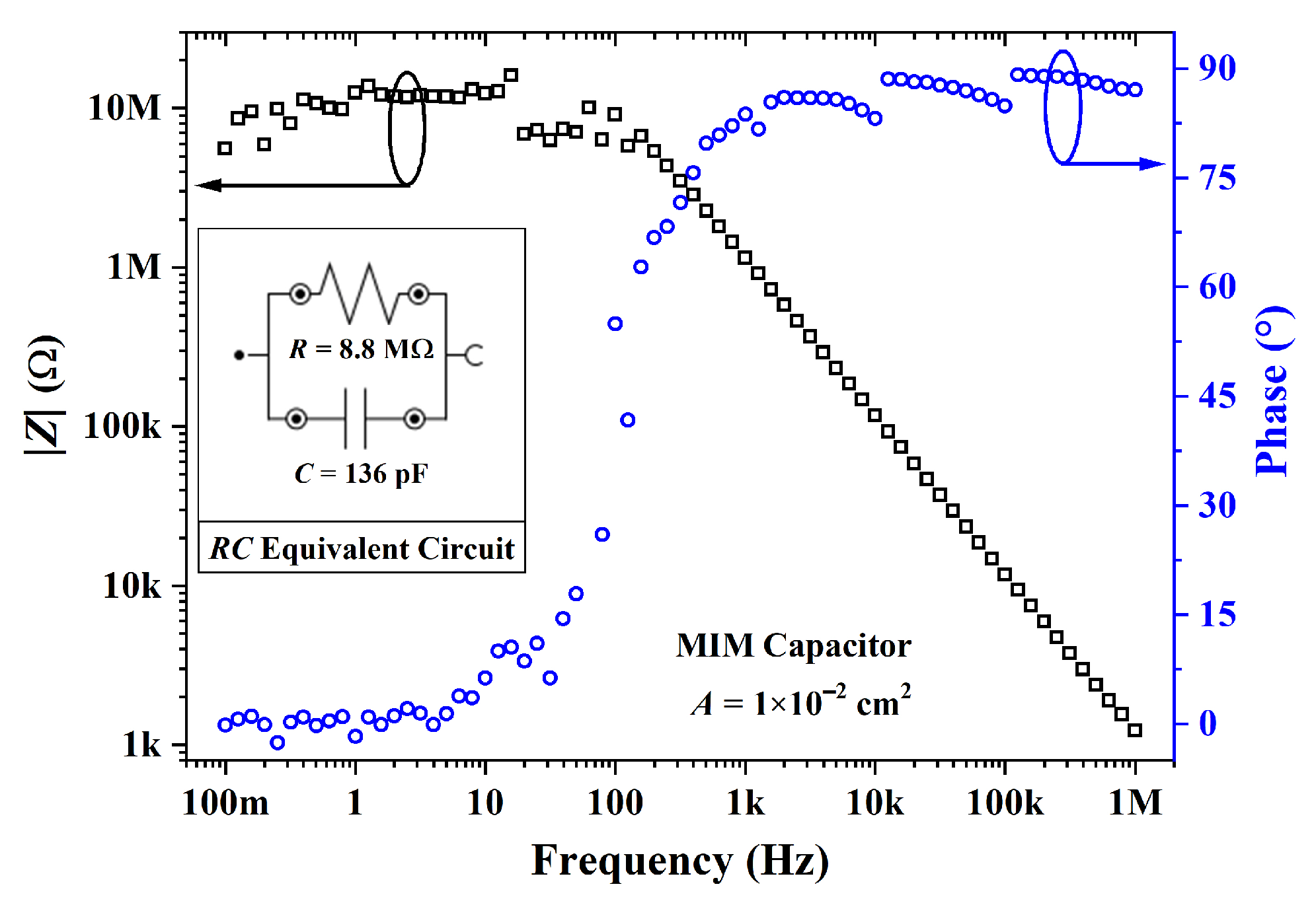
An MIM capacitor was processed from cross-linked PVP. The Bode diagram in
Figure 15 shows that the impedance was ca. 10 M
and
for frequencies in the range of 0.1 to 10 Hz. This purely resistive behavior gradually shifted to a purely capacitive one from 1 kHz to 1 MHz with an impedance phase of ca.
. By using a parallel RC circuit model, a dielectric constant of
was calculated. As expected, the film is a high
k, which is in agreement with previous results [
73,
88,
89]. The C-V curves of capacitors from cross-linked PVP are given in
Figure 16. As expected, the capacitance from an MIM structure, as shown in
Figure 16a, remained constant. In contrast, the addition of PBTTT-C14 in an MIS structure led to a lower capacitance with an increase in
(see
Figure 16b). There was a noticeable change in capacitance with gate bias due to the additional capacitive element in series originating from the depleted semiconductor. This behavior could not be observed at high frequencies (e.g., 1 MHz) due to the low charge-carrier mobility from the semiconductor.
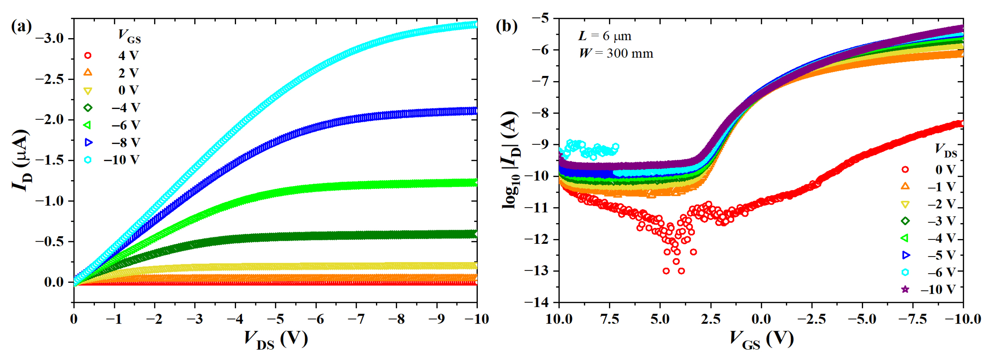
The leakage current density through the gate dielectric as a function of the electric field is given in
Figure 17. Its maximum absolute value was ca. 540 nA/cm
at
MV/cm (i.e., an
of approx. 9.8 nA at
V and
V), which is critical for OTFT operation in the cut-off region. High off currents are common in high-
k dielectrics, so a thin buffer layer is usually required for proper TFT operation [
73,
89]. Nevertheless, in this work, transistors were gas sensors operating in the triode region, in which the current in the channel (∼20–100 nA) was at least three orders of magnitude higher than the one through the gate dielectric (<20 pA).
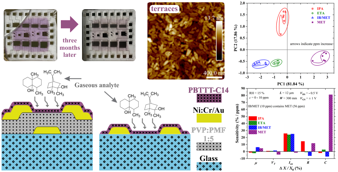
3.4. Gas-Sensing Response
The electrical parameters’ relative variation extracted from OTFTs’ transfer curves (see
Figure S6 in the Supplementary Materials) is reported in
Figure 19. Significant shifts for
,
, and
at 10 ppm were observed in the presence of MET (∼61%), MET (∼14%), and IB/MET (∼1000%), respectively. Mobility increased in the presence of MET and IB/MET but decreased when exposed to IPA and ETA. Threshold voltage and channel current always increased in the presence of alcohols and isoborneol.
At low analyte concentrations, the transistors were highly responsive to methanol and isoborneol. Under similar ppm levels, R varied ca. upon exposure to IPA, increasing both in the presence of IPA and MET, whereas decreasing in the presence of ETA and IB/MET. The capacitance, on the other hand, increased ca. upon exposure to MET, increasing both in the presence of MET and ETA, whereas it decreased in the presence of IPA and IB/MET.
At high concentrations (i.e., approaching 1000 ppm), significant shifts for , , and were observed in the presence of MET (∼76%), IPA (∼26%), and IB/MET (∼1740%), respectively. There was a clear saturation profile for OTFT parameters above 100 ppm. In any case, the transistors were also highly responsive to isopropyl alcohol. At these concentration levels, R increased ca. ∼260% upon exposure to IPA, whereas C increased ca. in response to MET. Chemical sensors also tend to saturate for concentrations greater than 100 ppm.
Table 6 was generated in order to assess the effect of measuring isoborneol in the presence of methanol. Except for
(∼3%), there was a noticeable difference between the response to IB/MET and pure MET. Chemical sensors can also clearly distinguish between these two analytes. As will be seen later, these conclusions are also supported by PCA and sensitivity data.
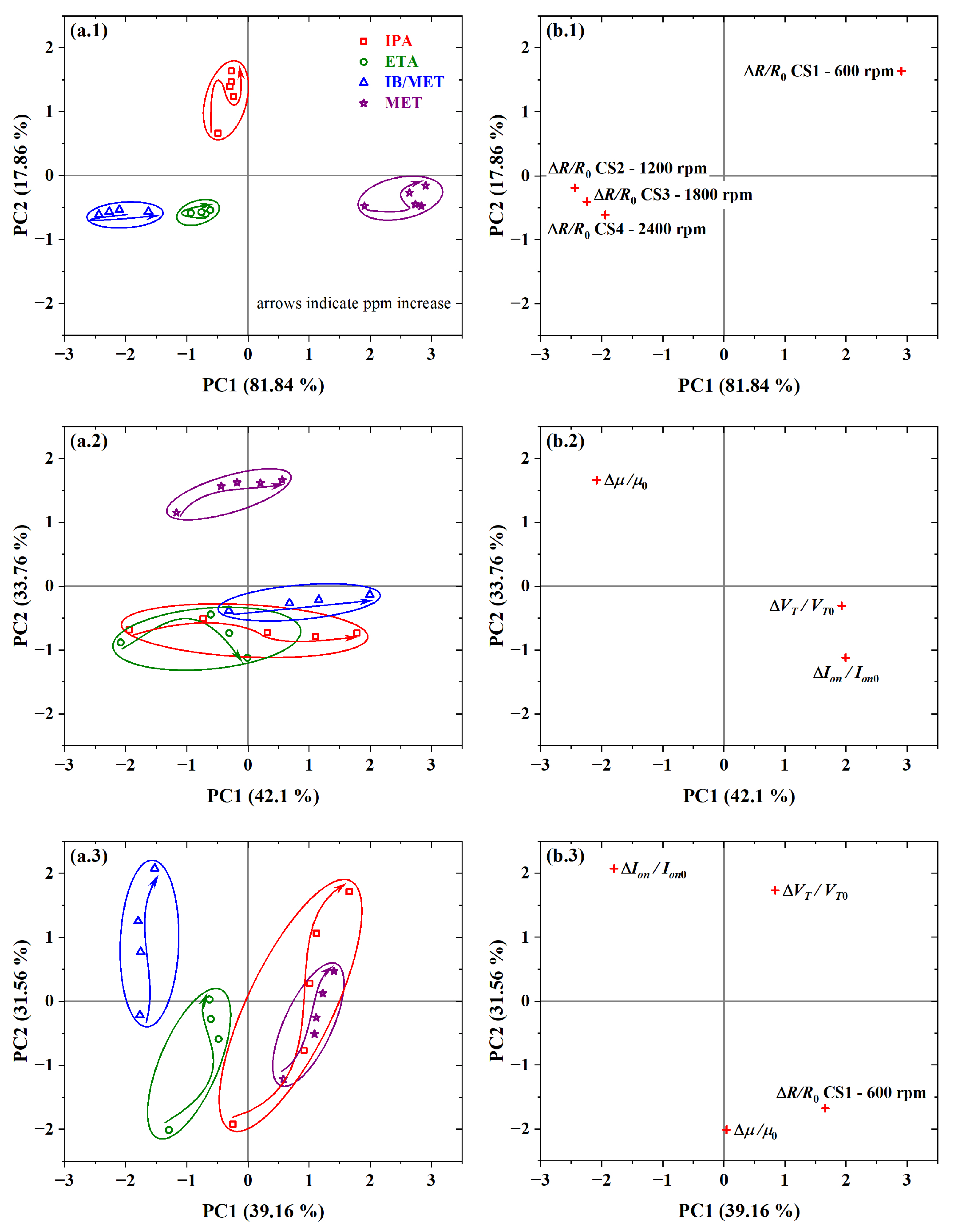
PCA plots are given in
Figure 20. By using only chemical sensors’ resistance data, a
of
and a sum (i.e.,
) of
was observed (see scores in
Figure 20(a.1)). It was possible to discriminate the four analyte samples into distinct clusters. In this case, there was also significant discrimination between the MET and IB/MET samples. This was the highest discrimination level observed for PCA bidimensional plots at hundreds of ppm of the investigated analytes.
The resistance of the chemical sensor from PBTTT-C14 spun at 600 rpm was detached from the ones from the other sensors (see loadings in
Figure 20(b.1)). The analysis of the loadings plot indicates that CS1 contributed the most to the discrimination of IPA along the PC2 axis. Additionally, CS1 contributed inversely to CS2, CS3, and CS4 in the discrimination along the PC1 axis. This points to a significant contribution coming from CS1, which is probably due to the thicker film and slower drying originating from the lower spinning frequency during deposition. Compared with MET and ETA, IPA has a lower dielectric constant (
) and dipole moment (
D) [
91]. It is likely that IPA penetrates deeper into the semiconducting film thanks to voids in the grain boundaries in a more crystalline structure, such as from CS1. In addition, a rougher surface from thicker films such as CS1 provides more interaction sites toward the detection of gaseous analytes. Similar behavior would be expected for IB, since it has an even lower dielectric constant (
[
92]) and dipole moment (
D [
93]). In this case, however, the larger molecular size of IB (0.50 nm [
94]) compared with the other analytes [
95,
96] might play a role against analyte diffusion into the sensing film.
The use or addition of capacitance data for the analysis worsens the discrimination ability of the system (see
Figure S7 in the Supplementary Materials). This agrees well with the fact that a zoom-in on
Figure 19e was necessary in order to distinguish among the response to IPA, ETA, and IB/MET. The higher selectivity of capacitance data to MET is probably related to its higher dielectric constant (
) and dipole moment (
D) with respect to the other investigated analytes [
91]. The average physicochemical properties of investigated analytes are summarized in
Table S5 in the Supplementary Materials.
Performing a PCA with only the transistors’ electrical parameters, such as
,
, and
, provided a
of
and a sum of
(see scores in
Figure 20(a.2)). In this case, there was the most significant overlap of clusters from different analyte samples along the PC1, such that the use of two PC axes provided only partial discrimination. Despite that, it was possible to separate MET and IB/MET on opposite sides of the plot. In addition, there should be enough MET in the IB solution to saturate the sensor response to that analyte. In this work, for each 10 ppm of IB, there are 56 ppm of MET only (i.e., approx. five times more). Therefore, at 100 ppm of IB, there is already 560 ppm of MET, i.e., more than enough for the response to be saturated from methanol. This is another clear indication that PBTTT-C14 TFTs respond to isoborneol. The reduced discrimination compared with CS points to better use of transistors at lower concentration levels (i.e., from units to tens of ppm). However, it should be noted that TFTs provide at least three significant parameters:
,
, and
. At the concentration levels used in this work, there is no reasonable gain by combining CS and OTFT data. In this case, both the PC1 and the sum decreased to
and
, respectively (see scores in
Figure 20(a.3)). For more details, see
Table S4 in the Supplementary Materials.
The reproducibility of chemical sensors from PBTTT-C14 films was also demonstrated in this work (see
Table S4 in the Supplementary Materials). The difference in the sum of the first two principal components was only
in PCA obtained from
R data,
from
C, and
from both
R and
C. The best combination of electrical parameters was achieved with
R,
, and
, which provided a
of
and a sum of
. One direct conclusion is that, despite the excellent attributes already described for the cross-linked dielectric, it interferes negatively with the discrimination of isoborneol through the OTFT’s threshold voltage.
The sensitivity calculated at the 10 ppm level for both OTFT and CS is shown in
Figure 21. Charge-carrier mobility enhances the discrimination of IB/MET and MET. It features a sensitivity of ca.
and
/ppm to IB/MET and MET, respectively. The threshold current and the channel current, on the other hand, assist mostly in the discrimination of MET with a sensitivity of ca.
and
/ppm, respectively. In agreement with an earlier discussion,
is highly sensitive to methanol, which impairs the discrimination of isoborneol. As expected,
R helps to separate IB/MET with a sensitivity of approx.
ppm, despite being highly sensitive to IPA too (∼14.5%/ppm).
C behaves similarly to
, being highly sensitive to MET (ca.
/ppm).
Multiple mechanisms of detection are believed to happen simultaneously within the organic material. For instance, polar molecules can become trapped in the PBTTT-C14 film and interact with charge carriers (i.e., holes) [
57,
97]. This interaction usually translates into a change in the potential barrier to transport and in the charge trapping along the channel. The analyte molecules are expected to physically adsorb onto the surface of the sensing semiconductor film, but also percolate through the voids surrounding the grains until they reach the dielectric surface [
57]. Notably, the degree of physisorption depends on the chemical affinity between the active layer and the analyte, occurring both in the bulk of the semiconducting film and at the interface with the dielectric [
57]. In summary, it has been shown that PBTTT-C14 is not only suitable for moisture and ammonia detection [
23,
37,
98], but also has enormous potential for alcohol detection and water quality assessment.


 ,
, 


