
Structure and Technological Parameters’ Effect on MISFET-Based Hydrogen Sensors’ Characteristics


Micro- and Nanoelectronics Department, National Research Nuclear University MEPhI (Moscow Engineering Physics Institute), Kashirskoe Highway 31, 115409 Moscow, Russia
*
Author to whom correspondence should be addressed.
Sensors 2023, 23(6), 3273; https://doi.org/10.3390/s23063273
Submission received: 16 February 2023
/
Revised: 14 March 2023
/
Accepted: 16 March 2023
/
Published: 20 March 2023
(This article belongs to the Special Issue Advanced Field-Effect Sensors: Volume II)
Abstract
:The influence of structure and technological parameters (STPs) on the metrological characteristics of hydrogen sensors based on MISFETs has been investigated. Compact electrophysical and electrical models connecting the drain current, the voltage between the drain and the source and the voltage between the gate and the substrate with the technological parameters of the n-channel MISFET as a sensitive element of the hydrogen sensor are proposed in a general form. Unlike the majority of works, in which the hydrogen sensitivity of only the threshold voltage of the MISFET is investigated, the proposed models allow us to simulate the hydrogen sensitivity of gate voltages or drain currents in weak and strong inversion modes, taking into account changes in the MIS structure charges. A quantitative assessment of the effect of STPs on MISFET performances (conversion function, hydrogen sensitivity, gas concentration measurement errors, sensitivity threshold and operating range) is given for a MISFET with a Pd-Ta2O5-SiO2-Si structure. In the calculations, the parameters of the models obtained on the basis of the previous experimental results were used. It was shown how STPs and their technological variations, taking into account the electrical parameters, can affect the characteristics of MISFET-based hydrogen sensors. It is noted, in particular, that for MISFET with submicron two-layer gate insulators, the key influencing parameters are their type and thickness. Proposed approaches and compact refined models can be used to predict performances of MISFET-based gas analysis devices and micro-systems.
1. Introduction
Many types of hydrogen sensors are used in fire–explosion safety and environmental monitoring systems [1]. The microminiaturization and intellectualization of such systems based on microtechnology and nanotechnology as well as improving their performance characteristics are the main trends of their development [2]. To develop the integrated hydrogen sensors and gas-analytic lab-on-chip systems, the sensitive elements must have technological compatibility with the elements of the integrated circuits. The capacitor and transistor elements based on metal–insulator–semiconductor (MIS) structures have good compatibility with the integrated circuits’ elements [3].
Gas sensors based on MIS capacitors and field-effect transistors (MISFETs) have been studied by many investigators. A great contribution to the developments of gas-sensitive MIS devices has been made by the researchers at Linköping University since their first work in 1975 [4]. Works [5,6] described the gas sensitivity mechanisms, the kinetic modeling of hydrogen adsorption/absorption in thin films of catalytic metals and the formation of hydrogen atom dipoles in the metal–SiO2 interfaces of MIS sensors. MIS sensors with different gate material (palladium [6], platinum and iridium [7]), with dielectric films SiO2, Si3N4-SiO2, TiO2-SiO2 and Ta2O5-SiO2 have been investigated [8]. The semiconductors Si [4,7], GaAs [3,9] and SiC [10] were used in MIS gas sensors to detect the low concentrations of gases H2 [6], NH3 [7], H2S [11], NO2 [12] and CO [13]. The studies have shown that performance characteristics of MISFET-based hydrogen sensors depend on technological parameters [8], electrical modes [14], chip temperature [15] and external factors (e.g., irradiation [16]).
Work on the study of the hydrogen effect on the properties of thin Pd films (less than 1 micron) began long before the appearance of real MISFET, and they are still ongoing. It has been shown that under the influence of various concentrations of hydrogen in the air, the partial pressure of the surrounding gases, the temperature and type of substrate, the thickness and deposition technology of the Pd film as a result of chemical reactions, changes in the structure, density and chemical composition of palladium films can occur [8]. As a result, under certain conditions of thermo-hydrogen exposure, PdxHy and PdO compounds are formed in palladium films, and the films themselves can swell and peel off from the substrate [17]. These effects lead to irreversible and/or reversible changes in the electrical conductivity of the films and the work of the electron output from Pd [3], which is the physical principle of operation of some types of hydrogen sensors.
In addition to these effects, the following processes are considered in the models of hydrogen sensitivity of MIS capacitors and MISFET. Firstly, the hydrogen molecules adsorb on the surface of the Pd film and then dissociate into atoms. The hydrogen concentration in Pd is proportional to the concentration of adsorbed hydrogen molecules in Pd and hydrogen concentrations in air, as well as dependent on Pd temperature and the concentrations of other molecules [18]. Secondly, there is the diffusion of hydrogen atoms through the Pd film to the Pd–insulator interface [6,19]. Some hydrogen atoms form PdxHy compounds, the concentration, structure and “lifetime” of which strongly depend on the chip temperature and hydrogen concentration [14]. Some hydrogen atoms penetrate to the boundary, with the dielectric either directly through the pores in the palladium film or via the tunnel mechanism through palladium grains (clusters) [5,11]. It is these atoms that form a polarized dipole layer of H in the Pd–insulator interface [6]. In work [20], based on modeling, doubts are expressed about the possibility of forming a dipole layer at the palladium–dielectric boundary. Third, there may be diffusion and drift protons in the insulator [21].
Thus, the hydrogen sensitivity of MIS devices depends on many factors. The simultaneous taking into account of all the factors is very difficult or not possible at all. In this article, the hydrogen sensitivity of the sensor characteristics was evaluated on the basis of a two-component physical model that takes into account possible changes in the work of the electron output from the gate material and changes in the MIS structure.
In recent years, based on nano- on micro-technologies, gas sensors with low sensitivity thresholds and low inertia have been developed. For example, new developments used nanostructured palladium films and Pd nanotubes [22], electrodeposited nanomaterials [23], nanoporous silicon thin films [24], integrated FET [25] and carbon nanotubes [26]. Microtechnologies, in combination with CMOS technologies [27,28], are used not only for the development of hydrogen and hydrogen-containing gas sensors [29], but also for the detection of other types of gases (e.g., CO [13,30] and NO2 [12,31]). Note that sensor developments [13,26] are based on functionalized Single-Walled Carbon Nanotubes (SWNTs).
The researchers at National Research Nuclear University MEPhI have developed and investigated the number of discrete and integrated gas sensors (MIS capacitors, Pd and Pt resistors) with Pd (or Pt)-SiO2-Si, Pd/Ti-SiO2-Si, Pd (or Pt)-Ta2O5-SiO2-Si structures. Experiments have demonstrated that MISFETs have the best performances compared to MIS capacitors and resistors. In addition, the integrated sensors, containing MISFET with a Pd(Ag)-Ta2O5-SiO2-Si-structure (hereinafter referred to as TSE), possess the best stability and reproducibility of characteristics [21]. In recent years, we have investigated the metrological and operating characteristics of TSE (e.g., electrical modes [14], chip temperature [15] and irradiation [16]).
In this paper, we have investigated the influence of the structure and technological parameters (STPs) on the characteristics of MISFET hydrogen sensors in a general form, and for TSE, based on refined compact models, allowing us to simulate the hydrogen sensitivity of gate voltages or drain currents in weak and strong inversion modes, taking into account changes in the work of the electron output from the gate material and charges in the MIS structure. A quantitative assessment of the effect of STP on the TSE conversion function, hydrogen sensitivity, gas concentration measurement errors, sensitivity threshold and operating range is given.
2. Materials and Methods
2.1. Initial Structure and Technological Parameters of TSE
The initial structure and technological parameters, which are considered unchanged when modeling sensor characteristics, included the dimensional parameters of the structural elements, the parameters of the semiconductor and the dielectric materials listed in Table 1. The STP values are determined using the specified materials, structure and topology of the TSE and are used to calculate the parameters C0, a and b of the TSE characteristic electrophysical models.
The errors in the calculations of electrophysical parameters depend on the errors of the STPs, which are determined using the technological standards or errors of the measuring instruments, if the values of the STPs were determined experimentally. For example, if ε3 is (12 ± 0.2), w is (3.2 ± 0.02) mm, L is (10 ± 0.1) μm, µn is (200 ± 5) cm2/(V∙s), NA is (5 ± 0.02) × 1015 cm−3, then the relative errors of the parameters C0, a and b are equal to 3.5%, 4.5% and 8.7%, respectively.
Denote the parameters with the symbol pk ∈ {pk} (k = 1, 2, …, 13 in Table 2). In general, the absolute and relative errors of the parameters Δpk and δpk are equal to ׀pkn − pk׀ and (Δpk/pkn) × 100%, respectively. The value of pkn is the desired (nominal) value of parameter pk or its average value, if this parameter was determined experimentally from a set of measured values.
The absolute errors of Δpk depend on the film manufacturing technologies (for parameters with indices k ∈ {1; 2; 3; 4; 5; 6}, on photolithography technologies (for p8, p9), on methods of estimating their thicknesses (for parameters with indices k ∈ {4; 5; 6} and on the type and structure of the materials (for parameters with indexes k ∈ {11; 12; 13}. Typically, the values of Δw and ΔL are in the range of 0.1 to 0.5 microns, and values Δd ∈ [5 nm; 15 nm] depend on d. The relative errors δw and δL are in the range from 0.002%...0.01% to 1.1%...5%. For specific technologies of the semiconductor wafers and dielectric films production, the relative errors δε1, δε2, δε3, δµn and δNA usually do not exceed 2%. The relative errors of δd1 and δd2 are in the range of δdmin ∈ [2%; 10%] to dmax ∈ [7.5%; 30%] and are the maximum for the STPs. Consequently, the thicknesses d1 and d2, the dimension of which will be determined in nm, can be considered the most critical STP.
2.2. Metrological Characteristics of TSE
To assess the influence of various factors on the characteristics of the sensors and systems being developed based on MISFETs, simulation modeling can be used, which is considered a fast and inexpensive method compared to full-scale tests of sensors with various STPs. In simulation modeling, the type, structure and values of STPs and the parameters of the models are chosen arbitrarily. In this paper, the characteristics of the TSE with the parameters specified in Table 1 were studied.
A fragment of the structure, the schematic designation of the n-channel TSE and a potentiometric circuit of its embedding for measuring the gas concentration C are shown in Figure 1 and Figure 2.
The main metrological characteristics of TCE include: conversion function (dependence V as function of C); differential Sd and integral S sensitivities being equal to dV/dC and ΔV/ΔC; absolute ΔC and relative δC errors of measurement C; the sensitivity threshold Cth; minimum relative error δCmin; the boundaries of the working range C1 and C2, limited by a given error δCmax and finally Cmax.
As previous studies [16,21] have shown, the conversion function of a TSE can be represented in general form as V (C) is [V0 − ΔV(C)], where the initial value of V (at C = 0) is equal to V0. In general, the output signals V of MISFETs-based sensors are formed as a result of the embedding of one or more transistors in various measurement circuits. In this paper, the main components of the models are determined using experimental studies of one TSE in the mode with a constant current ID and the voltage VD as shown in Figure 2b. In this case,
V (C) = VG (C) = VG0 − ΔVG (C) and Sd = dVG/dC,
VG0 (φs) = φs + a·{φs + φT·exp[(φs − 2φs0)/φT)]}1/2 + φms0 − [Qte0 + Qss (φs)]/C0.
For modeling the characteristics of TSE sensors, the following expression can be used to approximate the conversion function in the range of hydrogen concentrations from 0.005 vol.% to 1.5 vol.% [16]:
ΔVG(C) = ΔQte(C)/C0 − Δφms(C) = ΔVm · [1 − exp(−kC·C)] > 0.
Then, the sensitivity of Sd is equal to [−kC·ΔVm · exp(−kC·C)]. The maximum relative error of measuring the gas concentration δC in the general case is represented as
where Δ(C) is the absolute error of the specified gas concentration during sensor calibration, ΔV is the error voltage measurements and Δ(V) being equal to Δ(ΔVG) is the absolute voltage error associated with an absolute error of the parameter pk and is approximately equal to [dVG/dpk]·Δpk. Then, after sensor calibration the sensitivity threshold Cth is (ΔV/|Sdmax|), minimum relative error is δCmin and the boundaries of the working range C1 and C2 can be determined as solutions of Equations (5) and (6). The value of δCmin is δC (at C is C*), where C* is the solution of the following equation:
δC = 100% × ΔC/C = 100% × [Δ(C)·|Sd| + ΔV + Δ(V)]/(C|Sd|),
d(δC)/dC = 0.
The values of C1 and C2 are solutions of Equation (6) with respect to C at a given δCmax greater than δCmin:
δCmax = 100% × [Δ(C)|Sd| + ΔV + Δ(V)]/(C|Sd|),
Cmax = (1/kC) · ln (ΔVm/ΔV).
These transcendental equations will be solved using numerical methods. The testing n-channel MISFET based on the Pd-Ta2O5-SiO2-Si structure was fabricated on a single chip (2 × 2 mm2) together with a (p–n) junction temperature sensor and heater resistor by means of conventional n-MOS technology. Technological processes are detailed and presented in [14,21].
3. Results
3.1. Influence of Film Manufacturing Technology and Thicknesses on the Components of the Conversion Function
The experimental studies demonstrated that the MISFET hydrogen sensitivity depends on several effects, which occur in regions of the (ambient gas)–metal–dielectric structure. The probability of various effects depends on the following factors: chip temperature; partial pressure of hydrogen; material, chemical composition, structure, manufacturing technology and thickness of the gate film and the pressure of the gas medium [4,13,18,22,23]. The presence of a large number of influencing factors complicates and/or make it impossible in principle to simulate the influence of the material, the technology of production and the thickness of the shutter film on the metrological characteristics of MISFETs. The degree of this influence can only be determined experimentally. The morphology (crystalline, polycrystalline, amorphous, nanoparticles, etc.) of palladium films may affect the hydrogen sensitivity of sensors based on Pd film resistors or MIS structures as shown, for example, in [21,22].
Basically, the deposition technology and thickness of metal film dm can affect the conversion function components ΔQte(C) and Δφms(C). In the investigated TSE Pd film (dm is 70 ± 5 nm) was prepared using laser evaporation in vacuum 2·10−3 Pa in the substrate’s temperature range of 300–400 °C. For this technology, at thicknesses dm that is less than 80 nm, the palladium film has a porous structure. Therefore, it can be assumed that the hydrogen sensitivity and response time will be independent of dm and of its deviations Δdm from the nominal values of dmn. For other technologies (for example, with thicknesses of nanostructured Pd films less than 30 nm), the response time decreased, and the sensitivity can be increased at low concentrations (~5–50 ppm) with a decrease in dm [32]. Quantitative analysis of the effect of the Pd films’ characteristics on the hydrogen sensitivity of the TSE requires special experimental studies, which have not been observed in this work.
Deposition technologies and the thicknesses of dielectric films d1 and d2 can affect the conversion function components VG0 and ΔVm, which according to (2) and (3) are inversely proportional to specific capacity C0:
where in engineering physical models (8) and (9), the dimensions of the potentials are the volts, charge density is nCl/cm2, capacitance is nF/cm2 and thicknesses is nm. With an increase in the hydrogen concentration, the work of the electron output from Pd decreases, and therefore you have a negative value Δφms(C) [3]. The absolute ΔC0 and relative δC0 being equal to 100% × ΔC0/ΔC0 errors for C0 are, respectively, equal to:
where Δε1, Δε2, Δd1 and Δd2 and δε1, δε2, δd1 and δd2 are the absolute and relative errors of the corresponding values. For the values, ε1 is 25 and ε2 is 4, and the dependences of the components C0 and δC0 on thicknesses of d2 at different values of d1 are shown in Figure 3.
VG0 = φs + 0.085 + {41·[φs + 0.033·exp((φs − 0.42)/0.033)]1/2 − 5}/C0 (V),
ΔVm = ΔQtem/C0 − Δφmsm = 15/C0 + 0.11 (V),
C0 = (ε0ε1ε2)/(ε1d2 + ε2d1),
ΔC0 = ε0[ε2d1(Δε1·ε2 + 2Δε2·ε1) + ε1d2(Δε2·ε1 + 2Δε1·ε2) + ε1·ε2(Δd2·ε1 + Δd1·ε2)]/(ε1d2 + ε2d1)2,
δC0 = [δε1(2ε1d2 + ε2d1) + δε2(2ε2d1 + ε1d2) + δd2·ε1d2 + δd1·ε2d1]/(ε1d2 + ε2d1),
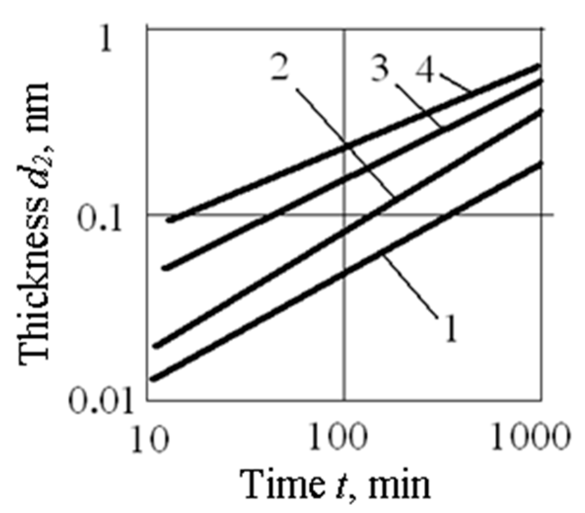
In the process of forming metal and dielectric films at a constant temperature Tp of the silicon wafer (substrate), their thicknesses depend on the time of the process t and on the temperature-dependent growth rate of the film vi. For example, when creating a SiO2 film via silicon oxidation in dry oxygen, the dependence of d2(t) for various Tp is shown in Figure 4 (based on Figure 8a in [32]). At the initial stage of silicon oxidation (up to d2 is about 30 nm), the thickness of the SiO2 film is proportional to the oxidation time t; with further oxidation, the thickness of d2 is proportional to (t)1/2. If the oxidation of silicon in dry oxygen is carried out at a temperature of 1100 °C, then the thickness d2 is v1·t (nm) at t ∈ [0; 10 min] and d2 = 30 + v2·(t)1/2 (nm) when the t is greater than 10 min, where v1 and v2 are equal to 4.0 nm/min and 8.5 nm·min ½; [t] is min.
The error δd2 is (δv2 + 100% × Δt/t) or δd2 is (δv2 + 50% × Δt/(t)1/2), where δv2 depends on the dispersion of the plate temperature ΔTp. The value of Δt is determined by the time parameters of the temperature response Tp (t) when the plate is introduced into the core with the constant temperature and partial pressure of oxygen, or by the time parameters of establishing a constant partial pressure of oxygen after oxygen is introduced into the placement zone of the plate heated to the operating temperature Tp and the time of oxygen pressure drop. Usually, δv2 < 0.5% and Δt ∈ (0.5; 2) min. For a given thickness d2, the error δd2 can be estimated as δd2 being less than the value of [0.5% + 425Δt/(d2 − 30)]. For example, if d2 is 50 nm and Δt is 30 s, then the value of δd2 < 11.1%, and if d2 is 80 nm and Δt is 30 s, then the value of δd2 < 4.75%.
Thus, the thicknesses and dielectric permittivities of dielectric films determine the capacitance C0, which can be considered a key parameter affecting the TSE conversion function.
3.2. Influence of Material’s Parameters and Topological Dimensions of Elements on Conversion Function Components
The material’s parameters (ε3, NA, µn) and topological dimensions (L, w) affect parameters a and b, which depend on the value of C0. According to (2), the conversion function component VG0 depends on the variables parameters a and φs. Then, the absolute error ΔVG0 with small deviations Δa and Δφs a from their average values can be presented as:
ΔVG0 = (∂VG0/∂φs)Δφs + (∂VG0 /∂a)Δa = 0.01·(Kφ·φs·δφs + Ka·a·δa),
Kφ = 1+ 0.5a(1+ exp m)/(φs + φT·exp m)1/2; Ka = (φs + φT·exp m)1/2; m = (φs − 2φs0)/φT.
Parameter a depends on values of ε3, NA and C0, and the potential φs depends on the given values of ID and VD. According to the simplified TSE electrical model [15], the dependence ID (VG) at φs > 2φs0 has two sections: parabolic when ID ∈ [ID0; ID1] and φs ∈ [2φs0; φs1], and linear when value of ID is greater than ID1 being equal to (ID0 + 0.5bVD2). In principle, the entire range of changes in the drain current ID and gate voltage VG corresponding to the inversion mode can be used to measure the hydrogen concentration. Usually, the values of the set current are within the error range: ID is IDn ± ΔID.
In practice, the electric mode of strong inversion (at φs > φs1) is chosen, in which the measurement errors ΔVG0 and δC are minimal. For example, when VD is 0.2 V (ID1 is 42 μA) and ID is equal to (20 ± 2) μA, the value of VG0 is (1.16 ± 0.01) V, and when ID is equal to (100 ± 2) μA, the value of VG0 is (1.25 ± 0.005) V. Then, the values of ID and fluctuations of Δφs are represented as:
ID = b·{a·VD·[(φs + φT exp m) 1/2 − φs1/2] − 0.5VD2}; Δφs ≈ 2ΔID·(φs + φT exp m)1/2/[a·b·VD·(1 + exp m)].
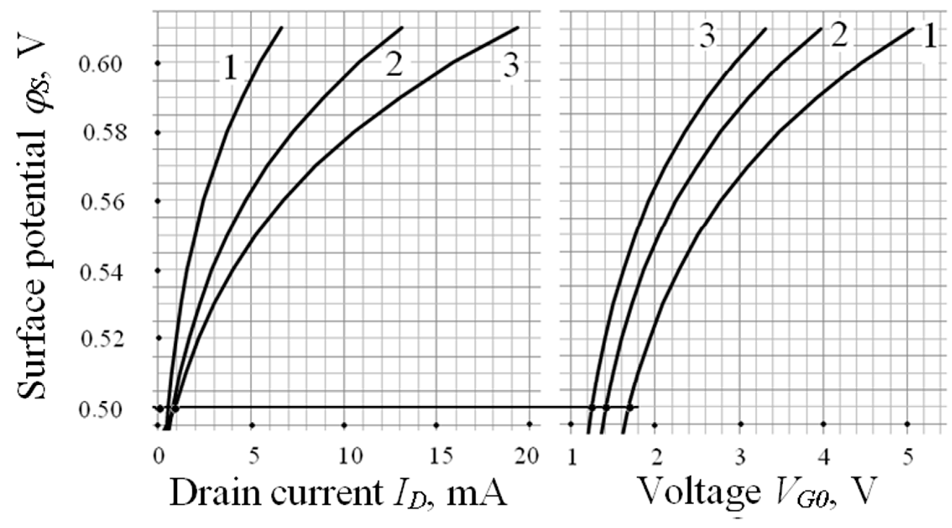
The dependences of the potential φs on the current ID at different VD and on values of VG0 at different C0 are shown in Figure 5. The relative errors of conversion function components a and b are equal to:
δa = δC0 + 0.5(δε3 + δNA) = 4.5% and δb = δC0 + δµn + δw + δL = 8.7%.
Quantitative values of a and b are given for the investigated TSE. Average values of the parameters of the conversion function for different C0 and (w/L) are presented in Table 3. As an example, Figure 5 shows the coordinates of the points corresponding to the values VG0 being equal to 1.2 V, 1.4 V and 1.7 V for different VD and a given drain current of 1 mA.
3.3. Influence of Specific Capacity on the Main Metrological Characteristics of TSE
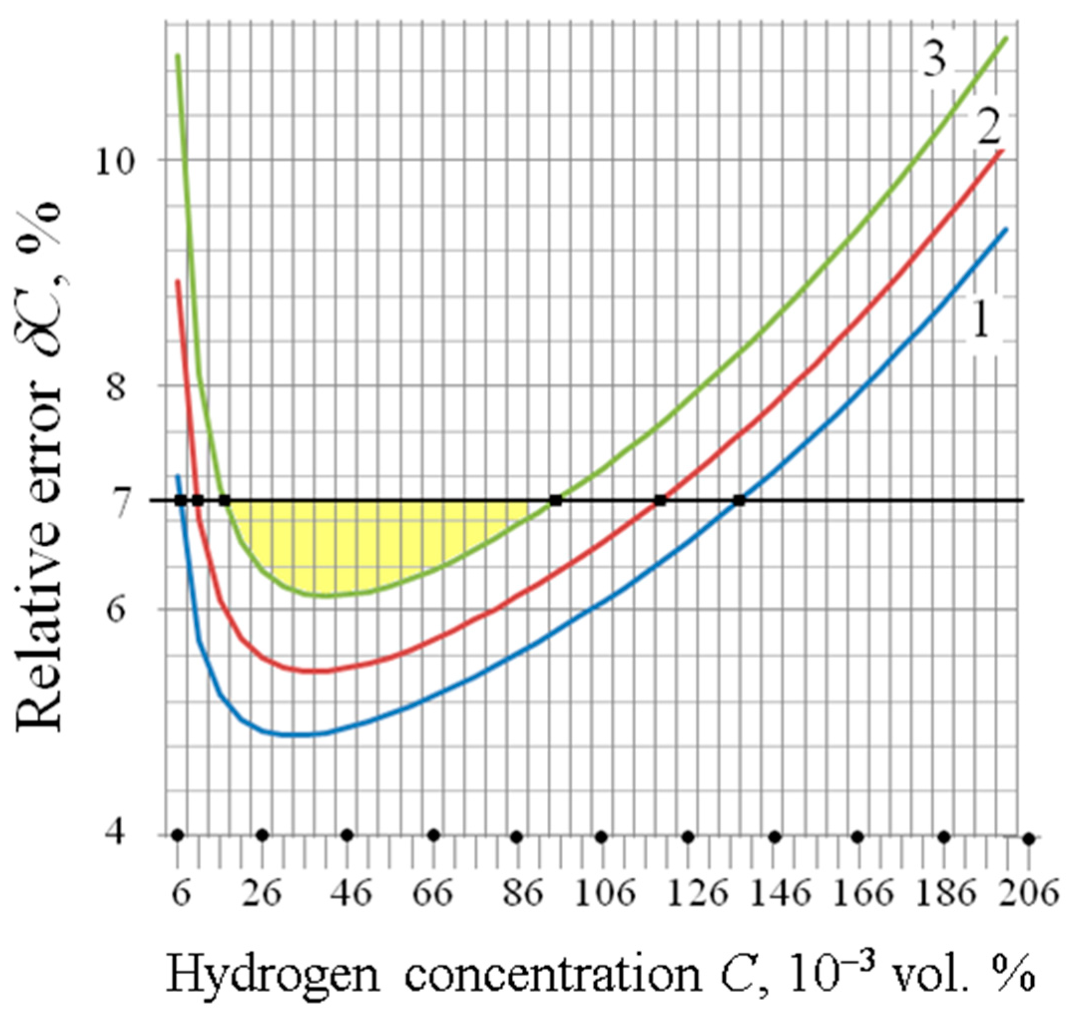
The quantitative assessment of the effect of STPs on the initial value of the output signal, hydrogen sensitivity, absolute and relative errors in measuring gas concentration, the sensitivity threshold, the maximum concentration and the hydrogen concentration range for a given maximum relative error is given. The calculations used engineering physical models obtained on the basis of selected electrophysical and electrical models. The dependences of δC(C) and the average values of metrological characteristics for different C0 are presented in Figure 6 and in Table 4.
4. Discussion
The analysis of the data obtained allows us to draw the following conclusions.
- All the considered STPs of the TSE (pk in Table 2) affect the components of the conversion function on which the main metrological characteristics depend.
- The deposition technology and thickness of the metal film dm can affect the conversion function components ΔQte(C) and Δφms(C) on which the sensor’s hydrogen sensitivity and the response time depend. A quantitative analysis of the effect of the Pd films technological characteristics on TSE hydrogen sensitivity requires special experimental studies. In the investigated TSE, the Pd film has a porous structure. Therefore, it can be assumed that the hydrogen sensitivity and response time will be independent of dm and of its deviations Δdm from the nominal values of dmn.
- The values of VG0 and ΔVG0 depend on NA, C0 and the given electrical parameters ID and VD. With the growth of ID and VD, the error ΔVG0 decreases. As a result of the calibration of the measuring device, the zero error is determined by the error ΔVG0 or the instrumental error of the voltage measurement ΔV (in the examples considered, ΔV is 1 mV).
5. Conclusions
Refined compact electrophysical and electrical models are proposed that link the drain current, the voltage between the drain and the source, the voltage between the gate and the substrate with the structure and technological parameters (STPs) of an n-channel MISFET as a sensitive element of a hydrogen sensor (TSE). The method of the analytical assessment of the effect of STPs on the main metrological characteristics of a TSE is proposed. A qualitative assessment is given of the influence of the metal gate film manufacturing technology, the technology of manufacturing the gate dielectric films and their thicknesses, the concentration of impurities in the semiconductor, the length and width of the channel and the mobility of electrons in the channel on the metrological characteristics of TCE.
Using the example of a TSE with a Pd-Ta2O5-SiO2-Si structure, manufactured according to a specific technology, a quantitative assessment of the effect of STPs on the initial value of the output signal, hydrogen sensitivity, absolute and relative errors in measuring gas concentration, the sensitivity threshold and the hydrogen concentration range for a given maximum relative error is given. The calculations used engineering physical models obtained on the basis of selected electrophysical and electrical models.
The degree of influence of each STP and their errors on the components of the conversion function and the main metrological characteristics of a TSE is shown. It has been established that for a specific technology of manufacturing TSEs (in particular, for MISFET with submicron two-layer gate insulators), the key influencing parameters are their type and thickness. Proposed approaches and models can be used to predict performances of MISFET-based gas analysis devices and micro-systems and also to solve the inverse problem determining the STPs according to the specified metrological characteristics.
Author Contributions
Conceptualization, B.P.; data curation, B.P. and M.E.; formal analysis, A.L.; funding acquisition, N.S.; investigation, M.E. and A.L.; methodology, B.P.; project administration, N.S.; resources, A.L.; supervision, N.S.; validation, M.E.; writing—original draft, B.P.; writing—review and editing, N.S. All authors will be informed about each step of manuscript processing including submission, revision, revision reminder, etc. via emails from our system or assigned Assistant Editor. All authors have read and agreed to the published version of the manuscript.
Funding
This work was supported by a grant from the Russian Science Foundation No. 18-79-10230.
Institutional Review Board Statement
Not applicable.
Informed Consent Statement
Not applicable.
Data Availability Statement
Data sharing not applicable.
Conflicts of Interest
The authors declare no conflict of interest. The funders had no role in the design of the study; in the collection, analyses, or interpretation of the data; in the writing of the manuscript; or in the decision to publish the results.
References
- Hübert, T.; Boon-Brett, L.; Black, G. Banach, U. Hydrogen sensors—A review. Sens. Actuators B 2011, 157, 329–352. [Google Scholar] [CrossRef]
- Hong, S.; Wu, M.; Hong, Y.; Jeong, Y.; Jung, G.; Shin, W.; Park, J.; Kim, D.; Jang, D.; Lee, J.H. FET-type gas sensors: A review. Sens. Actuators B 2020, 330, 129240. [Google Scholar] [CrossRef]
- Tejaswini, S.; Paresh, K. Work Function-Based MOS Hydrogen Sensor and its Functionality: A Review. Adv. Mater. Interfaces 2021, 8, 2100649. [Google Scholar]
- Lundström, I.; Shivaraman, S.; Svensson, C.; Lundkvist, L. A hydrogen-sensitive MOS field-effect transistor. Appl. Phys. Lett. 1975, 26, 55–57. [Google Scholar] [CrossRef]
- Lundström, I. Hydrogen sensitive MOS-structures, Part I: Principles and applications. Sens. Actuators 1981, 1, 423–426. [Google Scholar] [CrossRef]
- Lundström, I.; Armgarth, M.; Spetz, A.; Winquist, F. Gas sensors based on catalytic metal-gate field-effect devices. Sens. Actuators 1986, 3–4, 399–421. [Google Scholar] [CrossRef]
- Spetz, A.; Helmersson, U.; Enquist, F.; Armgarth, M.; Lundström, I. Structure and ammonia sensitivity of thin platinum or iridium gates in metal–oxide–silicon capacitors. Thin Solid Film. 1989, 177, 77–93. [Google Scholar] [CrossRef]
- Lundström, I.; Sundgren, H.; Winquist, F.; Eriksson, M.; Krants-Rülcker, C.; Lloyd-Spets, A. Twenty-five years of field effect gas sensor research in Linköping. Sens. Actuators B Chem. 2007, 121, 247–262. [Google Scholar] [CrossRef]
- Lin, K.W.; Cheng, C.C.; Cheng, S.Y.; Yu, K.H.; Wang, C.K.; Chuang, H.M.; Liu, W.C. A novel Pd/oxide/GaAs metal–insulator–semiconductor field-effect transistor (MISFET) hydrogen sensor. Semicond. Sci. Technol. 2001, 16, 997–1001. [Google Scholar] [CrossRef]
- Andersson, M.; Pearce, R.; Lloyd-Spetz, A. New generation SiC based field effect transistor gas sensors. Sens. Actuators B Chem. 2013, 179, 95–106. [Google Scholar] [CrossRef]
- Kalinina, L.; Litvinov, A.; Nikolaev, I.; Samotaev, N. MIS-Field Effect Sensors for low concentration of H2S for enviromental monitoring. Procedia Eng. 2010, 5, 1216–1219. [Google Scholar] [CrossRef] [Green Version]
- Yaqoob, U.; Younis, M.I. Chemical Gas Sensors: Recent Developments, Challenges, and the Potential of Machine Learning—A Review. Sensors 2021, 21, 2877. [Google Scholar] [CrossRef] [PubMed]
- Ren, Q.; Cao, Y.Q.; Arulraj, D.; Liu, C.; Wu, D.; Li, W.M.; Li, A.D. Resistive-Type Hydrogen Sensors Based on Zinc Oxide Nanostructures. J. Electrochem. Soc. 2020, 167, 067528. [Google Scholar] [CrossRef]
- Podlepetsky, B.; Nikiforova, M.; Kovalenko, A. Chip temperature influence on characteristics of MISFET hydrogen sensors. Sens. Actuators B 2018, 254, 1200–1205. [Google Scholar] [CrossRef]
- Podlepetsky, B.; Kovalenko, A.; Samotaev, N. Influence of electrical modes on performance of MISFET hydrogen sensors. Sens. Actuators B 2017, 248, 1017–1022. [Google Scholar] [CrossRef]
- Podlepetsky, B. Effect of irradiation on hydrogen sensors based on MISFET. Sens. Actuators B 2017, 238, 1207–1213. [Google Scholar] [CrossRef]
- Gurlo, A.; Clarke, D. High-Sensitivity Hydrogen Detection: Hydrogen-Induced Swelling of Multiple Cracked Palladium Films on Compliant Substrates. Angew. Chem. Int. Ed. 2011, 50, 10130–10132. [Google Scholar] [CrossRef] [PubMed]
- Eriksson, M.; Lundström, I.; Ekedahl, L.-G. A model of the Temkin isotherm behaviour for hydrogen adsorption at Pd–SiO2 interfaces. J. Appl. Phys. 1997, 82, 3143–3146. [Google Scholar] [CrossRef]
- Fogelberg, J.; Eriksson, M.; Dannetun, H.; Petersson, L.-G. Kinetic modeling of hydrogen adsorption/absorption in thin films on hydrogen-sensitive field-effect devices: Observation of large hydrogen-induced dipoles at the Pd–SiO2 interface. J. Appl. Phys. 1995, 78, 988–996. [Google Scholar] [CrossRef]
- Irokawa, Y.; Usami, M. First-Principles Studies of Hydrogen Absorption at Pd-SiO2 Interfaces. Sensors 2015, 15, 14757–14765. [Google Scholar] [CrossRef] [Green Version]
- Podlepetsky, B.I.; Kovalenko, A.V. Errors of Integrated Hydrogen Sensors based on FETs with Structure Pd-(Ag)–Ta2o5–Sio2–si. J. Electrochem. Soc. 2020, 167, 167524. [Google Scholar] [CrossRef]
- Li, X.; Le Thai, M.; Dutta, R.K.; Qiao, S.; Chandran, G.T.; Penner, R.M. Sub-6 nm Palladium Nanoparticles For Faster, More Sensitive H2 Detection Using Carbon Nanotube Ropes. ACS Sens. 2017, 2, 282. [Google Scholar] [CrossRef]
- Penner, R. A Nose for Hydrogen Gas: Fast, Sensitive H2 Sensors using Electrodeposited Nanomaterials. Acc. Chem. Res. 2017, 50, 1902–1910. [Google Scholar] [CrossRef] [PubMed]
- Kim, H.; Yun, J.; Gao, M.; Kim, H.; Cho, M.; Park, I. Nanoporous Silicon Thin Film-Based Hydrogen Sensor Using Metal-Assisted Chemical Etching with Annealed Palladium Nanoparticles. ACS Appl. Mater. Interfaces 2020, 12, 43614–43623. [Google Scholar] [CrossRef] [PubMed]
- Shin, W.; Hong, S.; Jung, G.; Jeong, Y.; Park, J.; Kim, D.; Lee, J.H. Improved signal-to-noise-ratio of FET-type gas sensors using body bias control and embedded micro-heater. Sens. Actuators B 2021, 329, 129166. [Google Scholar] [CrossRef]
- Guo, S.Y.; Hou, P.X.; Zhang, F.; Liu, C.; Cheng, H.M. Gas Sensors Based on Single-Wall Carbon Nanotubes. Molecules 2022, 27, 5381. [Google Scholar] [CrossRef]
- Usagava, T.; Takeyasu, K.; Fukutani, K. Hydrogen-Induced Dipoles and Sensing Principles of Pt-Ti-O gate Si-MISFET Hydrogen Gas Sensors. Procedia Eng. 2014, 87, 1015–1018. [Google Scholar] [CrossRef] [Green Version]
- Usagava, T.; Daugherty, D. Semiconductor Gas Sensor. U.S. Patent 20160097731A1, 7 April 2016. [Google Scholar]
- Sharma, B.; Sharma, A.; Kim, J. Recent advances on H2 sensor technologies based on MOX and FET devices: A review. Sens. Actuators B 2018, 262, 758–770. [Google Scholar] [CrossRef]
- Kumar, A.; Zhao, Y.; Mohammadi, M.M.; Liu, J. Palladium Nanosheet-Based Dual Gas Sensors for Sensitive Room-Temperature Hydrogen and Carbon Monoxide Detection. ACS Sens. 2022, 7, 225–234. [Google Scholar] [CrossRef]
- Saxena, P.; Shukla, P. A Review on Gas Sensor Technology and Its Applications. In Computational and Experimental Methods in Mechanical Engineering; Smart Innovation, Systems and Technologies; Rao, V.V., Kumaraswamy, A., Kalra, S., Saxena, A., Eds.; Springer: Singapore, 2022; p. 239. [Google Scholar]
- Available online: http://ece723.tripod.com/lec04.pdf.p.20 (accessed on 15 February 2023).
Disclaimer/Publisher’s Note: The statements, opinions and data contained in all publications are solely those of the individual authors and contributors and not of MDPI and/or the editors. MDPI and/or the editors disclaim responsibility for any injury to people or property resulting from any ideas, methods, instructions or products referred to in the content. |
Figure 1.
The structure and the schematic designation of TSE: 1 is gas-sensitive film, 2 is metal gate, 3 and 9 are drain and source contacts, 4 and 8 are passivating films, 5 and 10 are drain and source, 6 is substrate, 7 is channel, 11 is thin gate dielectric.
Figure 1.
The structure and the schematic designation of TSE: 1 is gas-sensitive film, 2 is metal gate, 3 and 9 are drain and source contacts, 4 and 8 are passivating films, 5 and 10 are drain and source, 6 is substrate, 7 is channel, 11 is thin gate dielectric.
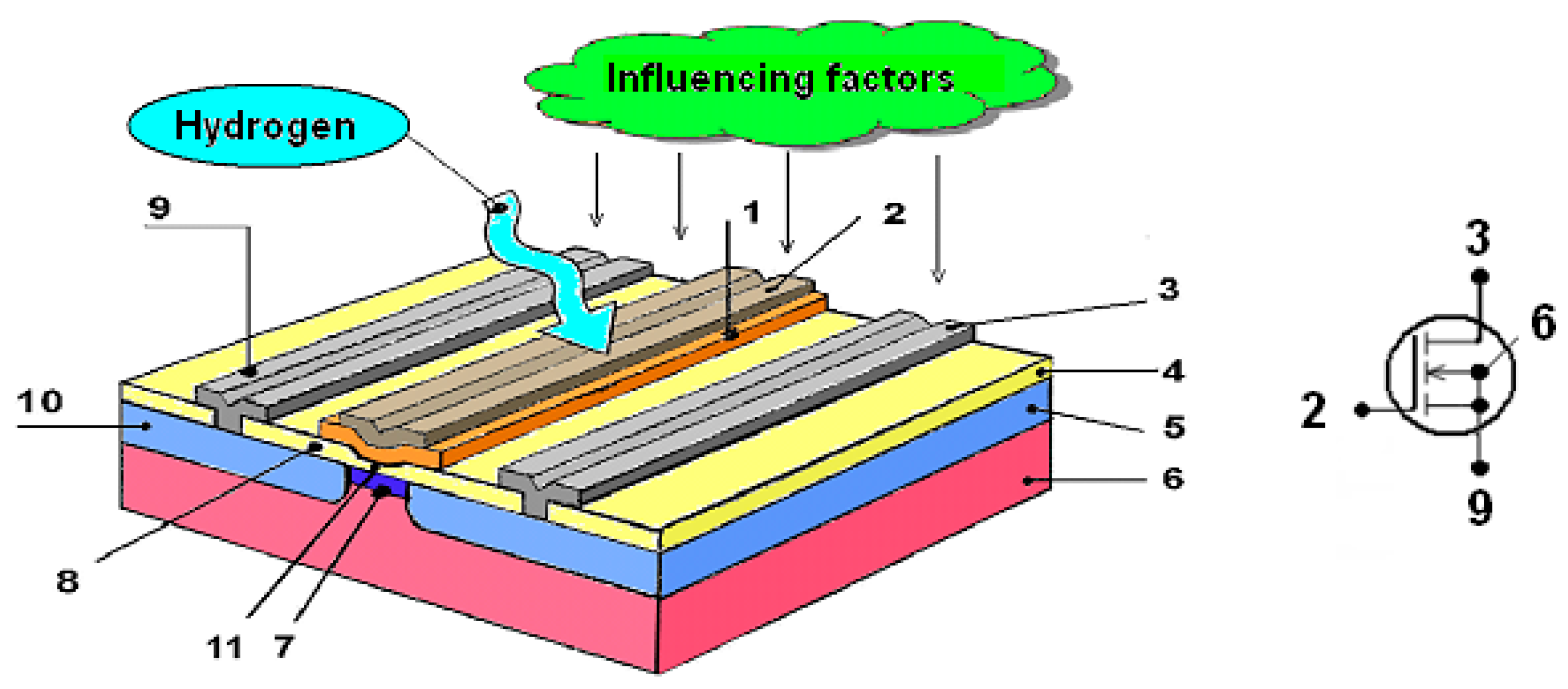
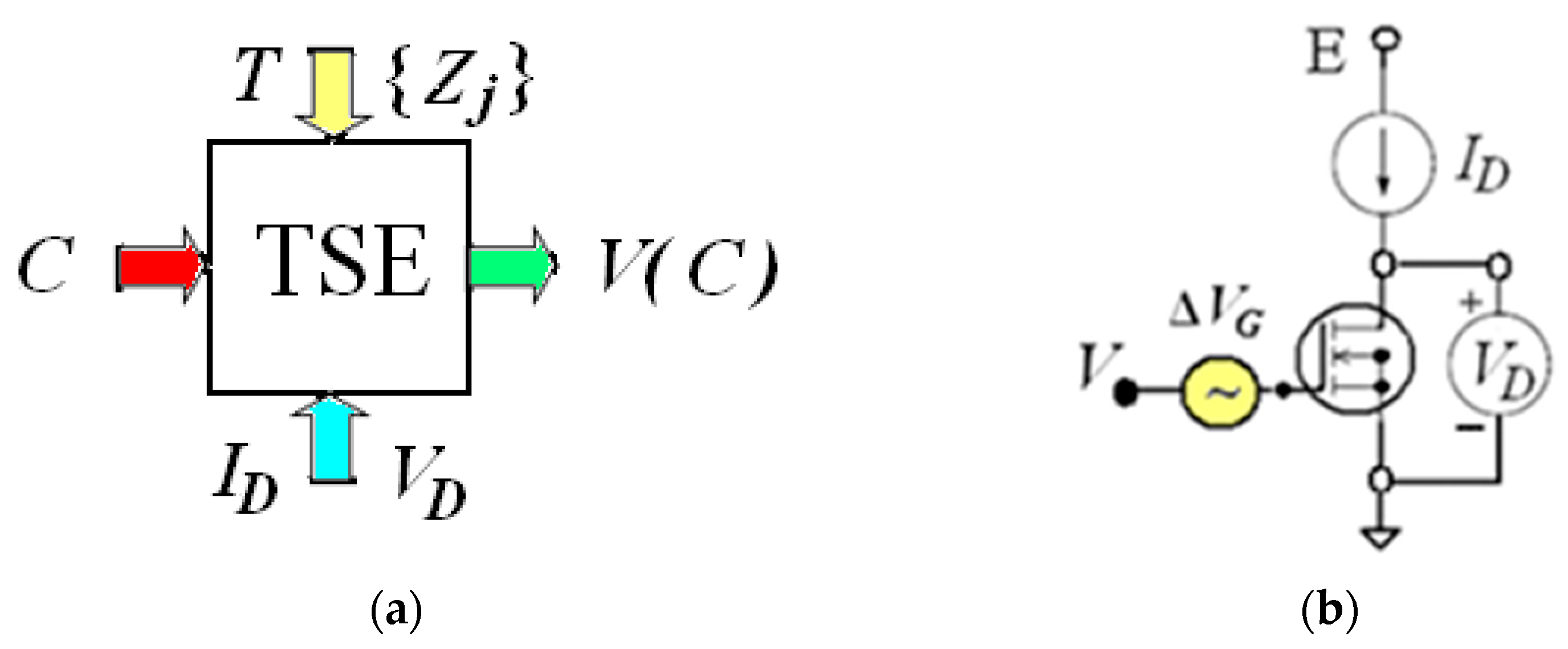
Figure 2.
(a) The input informative parameter is the gas concentration C; the output informative parameter is the voltage of the output signal V; the operating chip temperature is T; the parameters of the electrical mode of the circuit are the current ID and the voltage VD; external influencing factors {Zj} are molecules of other gases, temperature, humidity and radiation background of the environment. (b) The circuit for measuring the dependence V as function of C.

Figure 3.
(a,b) are dependences C0 (d2) and δC0(d2) at d1: 1 → 0 nm; 2 → 40 nm; 3 → 80 nm; 4 →120 nm.
Figure 3.
(a,b) are dependences C0 (d2) and δC0(d2) at d1: 1 → 0 nm; 2 → 40 nm; 3 → 80 nm; 4 →120 nm.
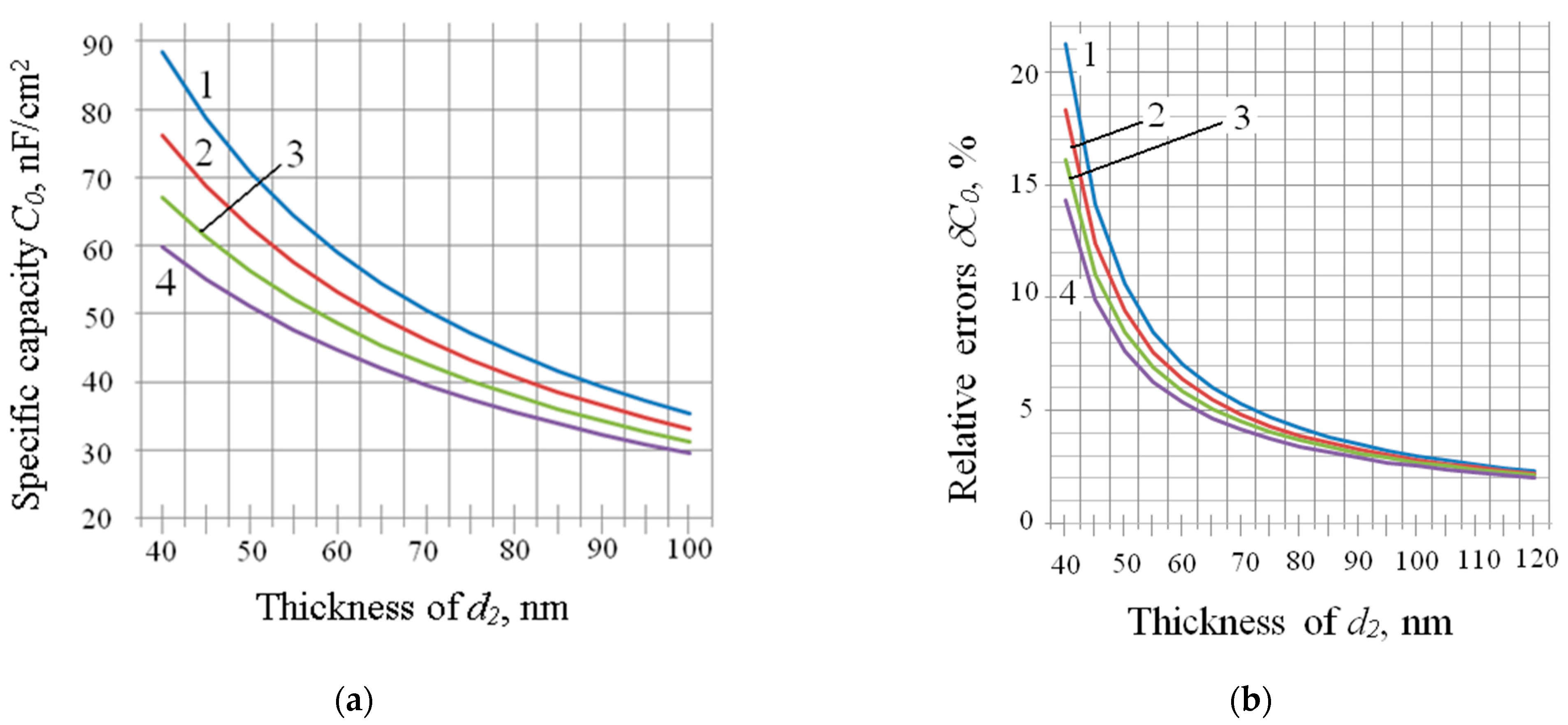
Figure 4.
Dependence of the SiO2 film thickness d2 on the oxidation time t in dry oxygen at temperatures: 1 → 900 °C; 2 → 1000 °C; 3 → 1100 °C; 4 → 1200 °C.
Figure 4.
Dependence of the SiO2 film thickness d2 on the oxidation time t in dry oxygen at temperatures: 1 → 900 °C; 2 → 1000 °C; 3 → 1100 °C; 4 → 1200 °C.

Figure 5.
Dependences of values φs on the current ID at different VD (1→ 0.1 V; 2 → 0.2 V; 3 → 0.3 V), and on values of VG0 at different C0 (1→ 30 nF/cm2; 2 → 40 nF/cm20.2 V; 3 → 50 nF/cm2).
Figure 5.
Dependences of values φs on the current ID at different VD (1→ 0.1 V; 2 → 0.2 V; 3 → 0.3 V), and on values of VG0 at different C0 (1→ 30 nF/cm2; 2 → 40 nF/cm20.2 V; 3 → 50 nF/cm2).

Figure 6.
Dependence of δC(C) for different C0: 1 → 30 nF/cm2; 2 → 40 nF/cm2; 3 → 50 nF/cm2. The values of C1 and C2 correspond to the square points on the curves. The color indicates the working area for the curve corresponding to the capacity of 50 nF/cm2.
Figure 6.
Dependence of δC(C) for different C0: 1 → 30 nF/cm2; 2 → 40 nF/cm2; 3 → 50 nF/cm2. The values of C1 and C2 correspond to the square points on the curves. The color indicates the working area for the curve corresponding to the capacity of 50 nF/cm2.


Table 1.
Average values of the parameters of MISFETs and parameters of used models.
| Symbols | Parameters | Values |
|---|---|---|
| Parameters of semiconductor and dielectric materials | ||
| ε1, ε2 and ε3 | relative permittivity of Ta2O5, SiO2 and Si | 25, 4 and 12 |
| NA | concentration of acceptors in Si | 5 × 1015 cm−3 |
| µn | electron mobility in the channel | 200 cm2/(V∙s) |
| Dimensions of structural elements | ||
| L and w | channel length and width | 10 μm and 3.2 mm |
| d1 and d2 | thicknesses of Ta2O5 and SiO2 | 90 nm and 80 nm |
| dm | thickness of the gate metal film | 70 nm |
| Constants and derived parameters | ||
| ε0 | dielectric constant of vacuum | 8.85 × 10⁻¹² F/m |
| k | Boltzmann constant | 1.38 × 10⁻²³ J/K |
| q | electron charge | 1.6 × 10⁻¹⁹ Cl |
| d | thickness of the gate dielectric is (d1 + d2) | 170 nm |
| ε | effective permittivity of the dielectric layer is (dε1ε2)/(ε1d2 + ε2d1) | 7.1 |
| C0 | specific capacity of the dielectric (ε0ε)/d | 37 nF/cm2 |
| a | charge parameter in Si is (2q ε0∙ε3∙NA)1/2/C0 | 1.18 V1/2 |
| b | specific steepness is (µnw C0)/L | 2 mA/V2 |
| Physical and electrical parameters | ||
| φms | output work difference potential Pd– Si | φms0 = 85 mV |
| T | chip temperature | 400 K |
| φT | thermal potential (kT/q) at 400 K | 33 mV |
| φgb | the potential of the band gap in Si | 1.08 V |
| φs0 | the potential of acceptors’ level is φT ln(NA/ni) at 400 K | 0.21 V |
| φs | surface potential is [φ(SiO2 − Si) − φF] | 0.2…0.8 V |
| Qte and Qss | charge densities in the dielectric and in SiO2 − Si interface | (5…100) nKl/cm2 |
| ID | drain current | (2…300) μA |
| VD | voltage between the drain and the source | (0.1…0.5) V |
| VG | voltage between the gate and the substrate | (1…3) V |
| Qte and Qss | charge densities in the dielectric and in SiO2 − Si interface | (5…100) nCl/cm2 |
| ID | drain current | (2…300) μA |
| VD | voltage between the drain and the source | (0.1…0.5) V |
| VG | voltage between the gate and the substrate | (1…3) V |
Table 2.
The effect of STP pk on the components of TSE models.
| k | STP | Components of TSE Models | |
|---|---|---|---|
| 1 | film production technologies | Pd | ΔQte (C); Δφms(C); φms0 |
| 2 | Ta2O5 | ΔQte(C); C0; b | |
| 3 | SiO2 | Qte0; Qss; C0; b | |
| 4 | film thicknesses | Pd (dM) | ΔQte (C); Δφms(C) |
| 5 | Ta2O5 (d1) | ΔQte(C); Qte0; C0; b | |
| 6 | SiO2 (d2) | Qte0; C0; b | |
| 7 | acceptor concentration | (NA) | a; φs0; Qss |
| 8 | channel length | (L) | b |
| 9 | channel width | (w) | |
| 10 | electron mobility in the channel | (µn) | |
| 11 | relative dielectric permittivity | Ta2O5 (ε1) | a; b; C0 |
| 12 | SiO2 (ε2) | ||
| 13 | Si (ε3) | ||
Table 3.
Average values of parameters for different C0 and (w/L) at ID is 0.1 mA and VD is 0.2 V.
| Parameters → | δC0, % | a, V | δa, % | w/L Is 0.003 | w/L Is 0.006 | ||||
|---|---|---|---|---|---|---|---|---|---|
| ↓ C0, nF/cm2 | b, mA/V2 | δb, % | ΔVG0, mV | b, mA/V2 | δb, % | ΔVG0, mV | |||
| 30 | 2.1 | 1.37 | 3.1 | 1.62 | 7.3 | 6 | 3.24 | 7.0 | 3 |
| 40 | 3.6 | 1.02 | 4.6 | 2.16 | 8.8 | 4.6 | 4.32 | 8.5 | 2.3 |
| 50 | 5.5 | 0.82 | 6.5 | 2.70 | 10.4 | 3.7 | 5.4 | 10.1 | 1.8 |
Table 4.
Average values of metrological characteristics for different C0 at δCmax being equal to 7%.
Table 4.
Average values of metrological characteristics for different C0 at δCmax being equal to 7%.
| MC → | VG0, V | ΔVm, V | kC, 1/(vol.%) | Sdmax, V/(vol.%) | δCmin, % | Cth, ppm | C1, ppm | C2, ppm | Cmax, ppm |
|---|---|---|---|---|---|---|---|---|---|
| ↓ C0, nF/cm2 | |||||||||
| 30 | 1.55 | 0.61 | 8 | 4.88 | 4.9 | 2.0 | 50 | 1410 | 8016 |
| 40 | 1.52 | 0.42 | 3.36 | 5.5 | 2.9 | 90 | 1210 | 7550 | |
| 50 | 1.48 | 0.32 | 2.56 | 6.1 | 3.9 | 160 | 960 | 7210 |
Disclaimer/Publisher’s Note: The statements, opinions and data contained in all publications are solely those of the individual author(s) and contributor(s) and not of MDPI and/or the editor(s). MDPI and/or the editor(s) disclaim responsibility for any injury to people or property resulting from any ideas, methods, instructions or products referred to in the content. |
© 2023 by the authors. Licensee MDPI, Basel, Switzerland. This article is an open access article distributed under the terms and conditions of the Creative Commons Attribution (CC BY) license (https://creativecommons.org/licenses/by/4.0/).
Share and Cite
MDPI and ACS Style
Podlepetsky, B.; Samotaev, N.; Etrekova, M.; Litvinov, A. Structure and Technological Parameters’ Effect on MISFET-Based Hydrogen Sensors’ Characteristics. Sensors 2023, 23, 3273. https://doi.org/10.3390/s23063273
AMA Style
Podlepetsky B, Samotaev N, Etrekova M, Litvinov A. Structure and Technological Parameters’ Effect on MISFET-Based Hydrogen Sensors’ Characteristics. Sensors. 2023; 23(6):3273. https://doi.org/10.3390/s23063273
Chicago/Turabian StylePodlepetsky, Boris, Nikolay Samotaev, Maya Etrekova, and Artur Litvinov. 2023. "Structure and Technological Parameters’ Effect on MISFET-Based Hydrogen Sensors’ Characteristics" Sensors 23, no. 6: 3273. https://doi.org/10.3390/s23063273
Note that from the first issue of 2016, this journal uses article numbers instead of page numbers. See further details here.