Article

Buck Converter with Cubic Static Conversion Ratio †

by
Delia-Anca Botila
*,
Ioana-Monica Pop-Calimanu
and
Dan Lascu
Applied Electronics Department, Politehnica University Timisoara, 300223 Timișoara, Romania
*
Author to whom correspondence should be addressed.
“Cubic Buck-Boost Converter with High Step-Up Capability” presented at the 2022 International Symposium on Electronics and Telecommunications (ISETC) conference, Timisoara, Romania, 10–11 November 2022.
Sensors 2024, 24(2), 696; https://doi.org/10.3390/s24020696
Submission received: 28 November 2023 / Revised: 16 January 2024 / Accepted: 18 January 2024 / Published: 22 January 2024

Abstract

:
The paper introduces a step-down converter that exhibits a static conversion ratio of cubic nature, providing an output voltage which is much closer to the input voltage, and at the same duty cycle, compared to a wide class of one-transistor buck-type topologies. Although the proposed topology contains many components, its control is still simple, as it employs only one transistor. A dc analysis is performed, the semiconductor stresses are derived in terms of input and output voltages and output power, revealing that the semiconductor voltage stresses remain acceptable and anyway lower than in other cubic buck topology. All detailed design equations are provided. The state-space approach is used to analyze the converter in the presence of conduction losses and a procedure for calculating the individual power dissipation is provided. The feasibility of the proposed cubic buck topology is first validated by computer simulation and finally confirmed by an experimental 12 V–10 W prototype.

1. Introduction

In applications that require a step-down of the input voltage, buck-type topologies are the first choice due to their compact size and ability to handle varying loads [1,2]. They are commonly used in various electronic devices and applications where efficient power converters are necessary, like power supplies [3,4], battery charging [5,6,7,8,9,10,11], IoT applications [12,13], LED drivers [14,15,16] and renewable energy [17].
An interesting topology that is using the basic principle of the conventional non-isolated buck converter is presented in [18]. It contains a reduced number of components compared to the classical one due to the use of an optocoupler as a switching device and thus the diode is not used.
Another topology with a single switch, but in this case with an increased number of diodes (four), two inductors and three capacitors, and that belongs to the non-linear voltage gain family, is the single-switch semi-quadratic buck converter proposed in [19].
Also, the quadratic converter presented in [20] exhibits only one transistor, three diodes, two inductors and two capacitors. Compared to the semi-quadratic converters, the number of diodes and capacitors is decreased, and the static conversion ratio is lower than the classical buck at the same duty cycle.
In article [21], a systematic method of constructing various types of quadratic converters is introduced by inserting a three-terminal, four-element switching cell into conventional switching cells, enabling the redevelopment of known converters and proposing new topologies.
A family of single-switch PWM converters that has a wide voltage range between the input and output is presented in [22]. The proposed converters exhibit reduced current stress compared with other step-down topologies mentioned in the paper.
Some PWM switched-capacitor converters featuring a switched-capacitor-inductor cell for adjustable high step-down voltage conversion were reported in [23]. The authors performed a useful comparison with different converter topologies, while taking into account the advantages and disadvantages of each circuit.
In papers [24,25,26], different step-down topologies, where the output voltage is closer to the input voltage, are presented. Emphasizing the study of a dc conversion ratio using mathematical tools, paper [24] generalizes a two-stage stacked step-down converter to an n-stage topology. The study from [25] introduces a family of switching step-down dc–dc converters based on the principle of reduced redundant power processing. The authors in [26] present a novel switched step-down dc–dc converter suitable for applications which require a small voltage difference between input and output. The converter demonstrates a measured efficiency of approximately 90% over a wide duty cycle range.
The authors from [27] present a single-input, double-output, unidirectional and bidirectional dc–dc buck converter. The paper shows the control strategy, PWM implementation and design specifications. A dual-output converter integrating two inductors into one magnetic coil, which is claimed to have a good dynamic behavior, is proposed in [28]. Another paper, [29], introduces a dual-output, high step-down converter with six active switches that has the advantages of improved efficiency through zero-voltage switching, compatibility with an existing buck controller integrated circuit, the ability to control multiple output voltages with a single controller and can be extended to more than two output rails.
A multiphase, synchronous buck converter is introduced in [30]. This converter employs two types of fully integrated current sensing schemes, as described in the paper.
The interleaved converter with coupled inductors from [31] has three windings built within a single core. The advantages of this converter, over other topologies, are also presented in the paper. A high step-down dc–dc converter with continuous output current, which maintains the soft switching of the semiconductors through a broad power range and reduces the MOSFET peak current with coupled inductors and series capacitors, is introduced in [32].
The authors of [33] analyzed some multilevel cascaded dc–dc converters for photovoltaic applications, together with some half-bridge topologies. One of those circuits is the multilevel cascaded dc–dc buck converter and another one is represented by the half-bridge buck converter. The main conclusion resulting from the paper is that, for series operation of photovoltaic generators, the buck topology is a proper choice, and, in the cascaded photovoltaic systems, the half-bridge topology of the buck converter is preferred. Another cascaded buck converter that improved efficiency by repositioning the second-stage inductor, reducing the total volume and conduction losses of the magnetic components, is introduced in [34].
An extended and comprehensive comparison of a variety existing step-down topologies, from which it can be remarked that cubic buck converters are not very common, is presented in [35]. In [36], the authors introduced a single-switch cubic buck converter and they recommend to use this topology for low power loads.
The present paper introduces a new cubic buck-type topology. It extends the authors’ previous research [37], where an ideal buck-boost topology of cubic nature is theoretically analyzed and verified only at a computer simulation level. Starting from the same parent converter [38], similar to the one from [37], the authors propose a cubic topology, this time of step-down nature, which is obtained using the same switching cell method. The content of the present paper is related to aspects that refer to:
  • The dc analysis for the ideal converter, together with the semiconductor stresses and ripples calculation;
  • The expression of the duty cycle for which a conversion from a given input voltage Vg to a desired output voltage Vo is achieved;
  • A comprehensive comparison of the proposed converter with other buck-type topologies, revealing superior features, at least compared to the cubic topologies;
  • The continuous conduction mode (CCM) operation conditions for a proper design of the inductors;
  • The analysis of the non-ideal converter in the presence of conduction losses with the help of the state-space matrices. The abovementioned, together with the design equations, can be found in Section 2;
  • A simulation for validating the theoretical operation of the ideal converter, as well as the experimental results on a 12 V–10 W prototype all confirm the feasibility of the proposed topology. These aspects are presented in Section 3;
  • The discussions and conclusions, which are included in Section 4 and Section 5, respectively.

2. Materials and Methods

The proposed cubic buck converter was derived from the cubic boost topology presented in [38]. Starting from its schematic, the proposed circuit was obtained by applying the three terminals switching cell rotation technique [39].
Basically, this method implies that the cell containing the switching devices and the reactive elements has three terminals which are connected to the supply voltage terminal (G), load terminal (L) and to the common point (C) of the circuit, as displayed in Figure 1. After the cell is extracted from the original converter, the semiconductors are swapped with single-pole single-throw (SPST) switches, maintaining the same control sequence. The next step is to obtain new circuits by rotating the resulting cell between the terminals G, L, C. Finally, after performing all five possible cell rotations, for each resulting topology, switch synthesis is performed, and the SPST switches are replaced by the corresponding semiconductor devices.
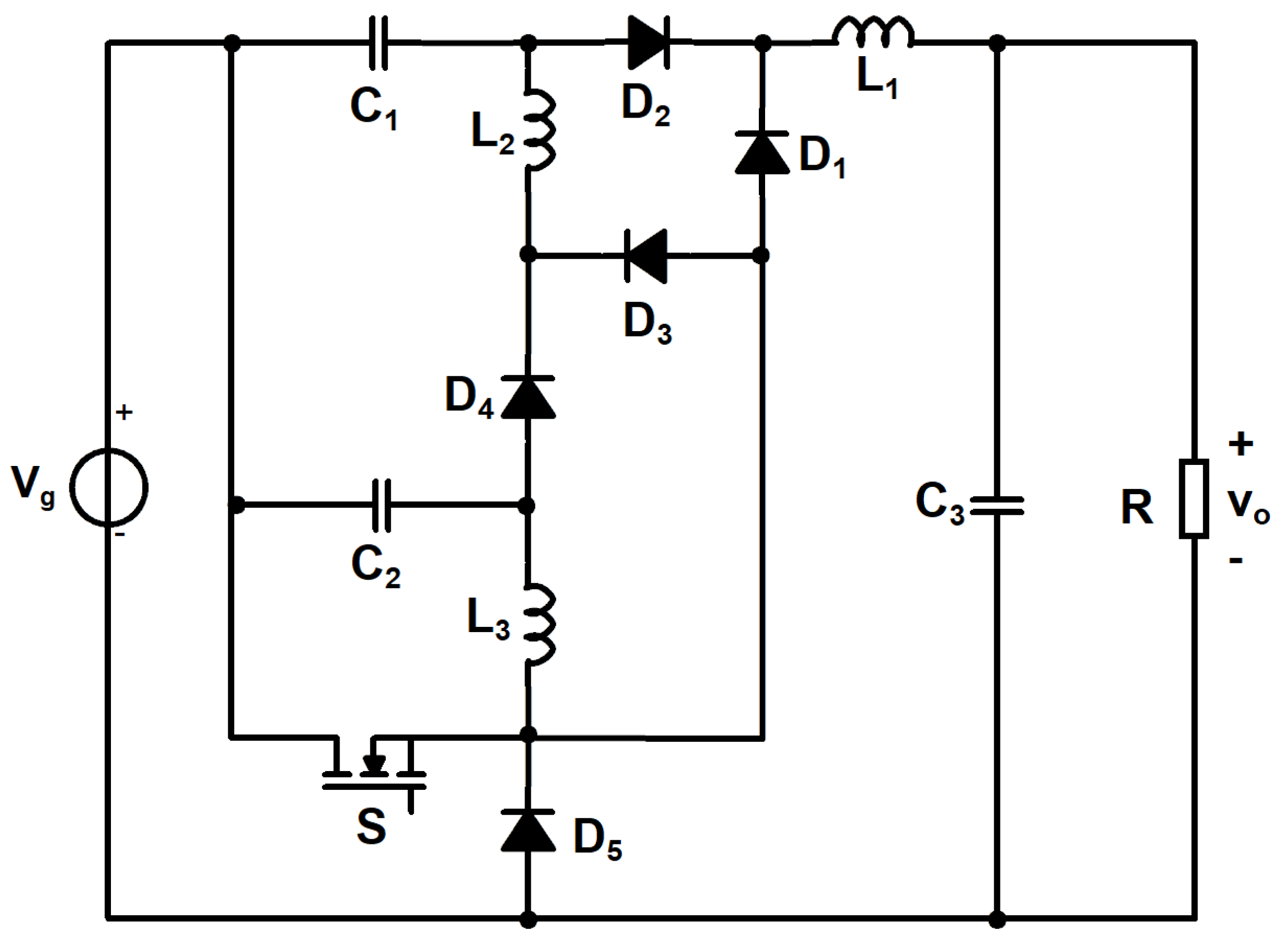
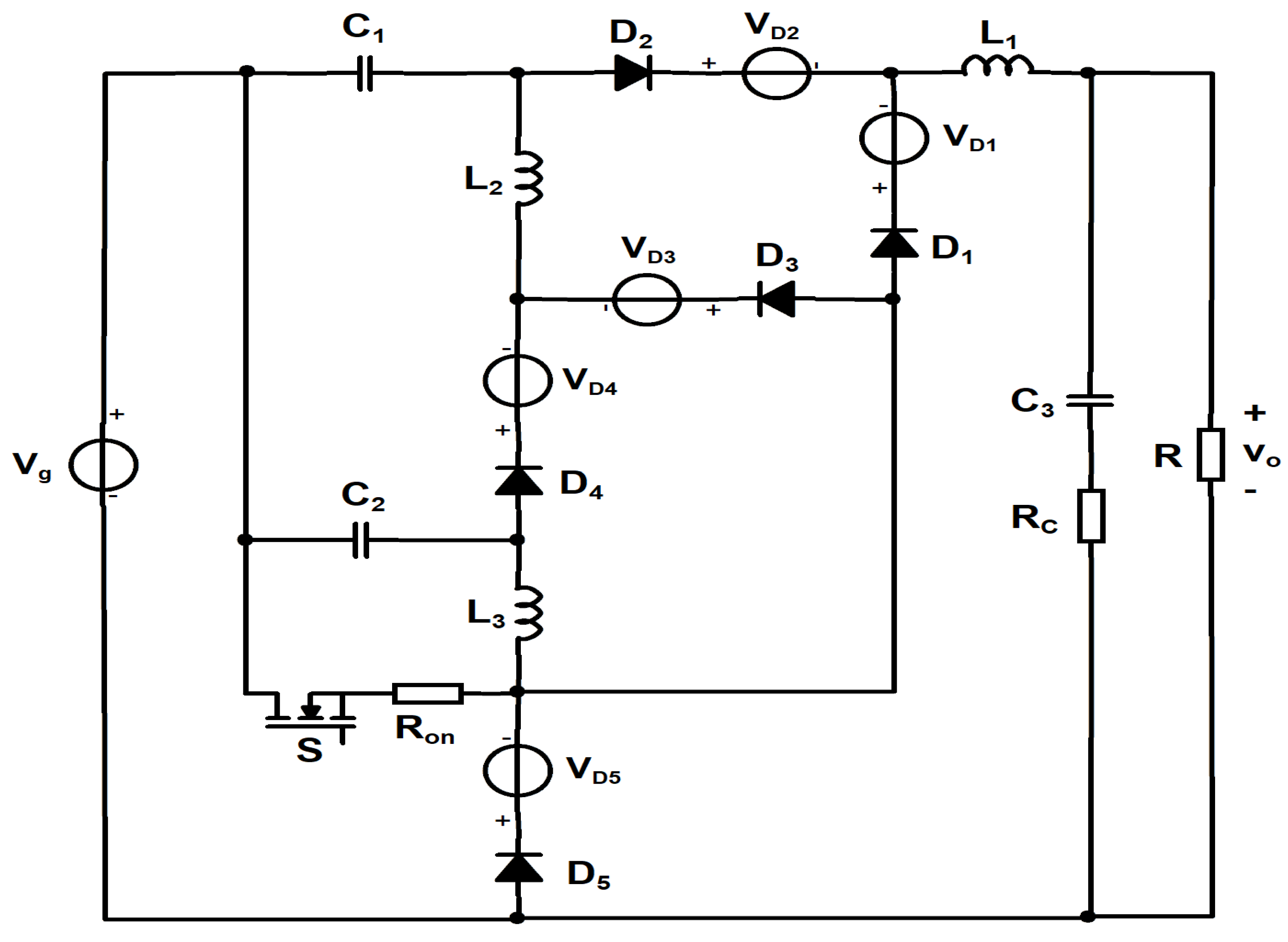
As a consequence, by applying the technique, which was previously described, the proposed converter, in its final form, is obtained for the combination 1-L, 2-C, 3-G connection and its schematic is presented in Figure 2. This new converter is first analyzed assuming ideal components, invoking the small ripple assumption for inductor currents and capacitor voltages and CCM operation. The transistor switching function q(t) is a pulse width modulated (PWM) signal of duty cycle D and switching frequency fS corresponds to the switching period TS.
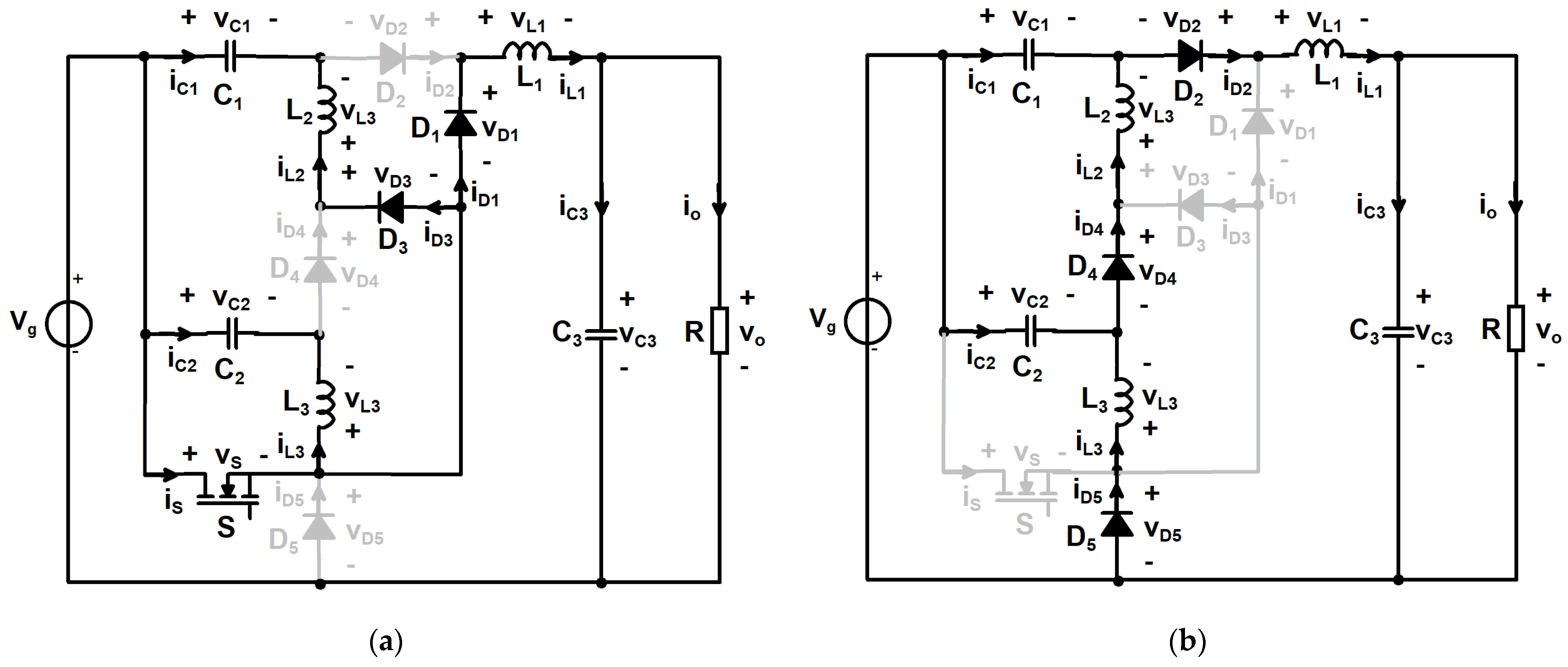
In the first topological state, which extends from 0 to D∙TS, the transistor conducts alongside diodes D1 and D3. The remaining amount of time until reaching a complete switching period, which is from D∙TS to TS, corresponds to the second topological state, in which the transistor is off and only diodes D2, D4 and D5 are forward biased and conducting. The schematics associated to each topological state are depicted in Figure 3.
In order to apply the volt-second balance principle to obtain the dc capacitor voltages, the dc voltage across each inductor shall be determined from both topological states. It results that:
D ( V g V C 3 ) + ( 1 D ) ( V g V C 3 V C 1 ) = 0
D V C 1 + ( 1 D ) ( V C 1 V C 2 ) = 0
D V C 2 + ( 1 D ) ( V g + V C 2 ) = 0
The capacitor currents are determined in each topological state and thus, the charge balance principle can be used to derive the dc inductor currents values:
D ( I L 2 ) + ( 1 D ) ( I L 1 I L 2 ) = 0
D ( I L 3 ) + ( 1 D ) ( I L 2 I L 3 ) = 0  
D ( I L 1 V C 3 R ) + ( 1 D ) ( I L 1 V C 3 R ) = 0  
Therefore, from (1) to (3), the dc capacitor voltages are obtained, along with the static conversion ratio:
V C 1 = ( 1 D ) 2 V g  
V C 2 = ( 1 D ) V g
V C 3 = V o = D · ( D 2 3 · D + 3 ) V g
M = V o V g = D · ( D 2 3 · D + 3 ) = 1 ( 1 D ) 3
For a given conversion from an input voltage Vg to a desired output voltage Vo, according to (10), the necessary duty cycle is:
D = 1 1 V o V g 3
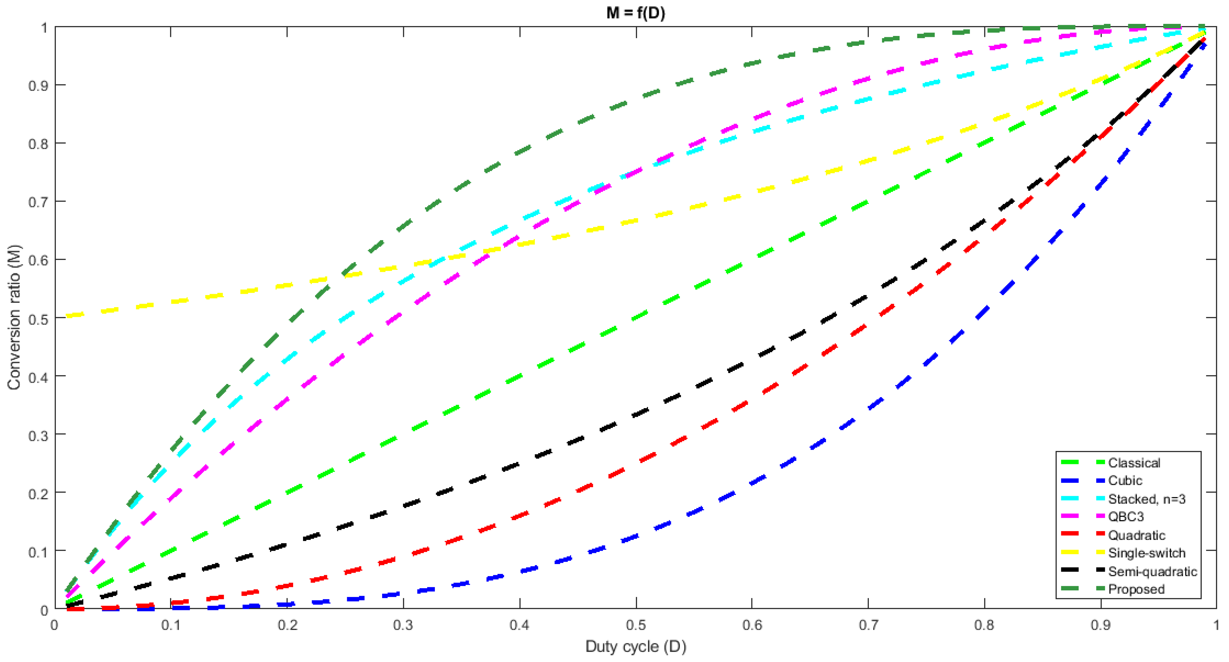
Equation (10) describes a static conversion ratio that is typical to a step-down converter topology, as it is always less than unity. In order to better show the step-down nature of the proposed circuit, its static conversion ratio dependency on the duty cycle is depicted in Figure 4, together with the ones corresponding to the classical buck [1], cubic buck [36], stacked buck [24], QBC3 [25], the quadratic buck [20], single-switch buck [26] and the semi-quadratic buck [19] converters.
Starting from this representation, it can be observed that, for any duty cycle, the proposed topology exhibits the highest static conversion ratio compared to the all of the mentioned converters. This feature ensures that the proposed cubic buck converter can be used in various applications where a low step-down of the input voltage is needed.
From Equations (4) to (6), the dc inductor currents are obtained, using also the dc capacitor voltages previously derived:
I L 1 = D · ( D 2 3 · D + 3 ) · V g R  
I L 2 = D · ( 1 D ) · ( D 2 3 · D + 3 ) · V g R
I L 3 = D · ( 1 D ) 2 · ( D 2 3 · D + 3 ) · V g R
It has to be mentioned that using (11) and replacing R by V o 2 P o , the dc capacitor voltages and inductor currents can be expressed only in terms of Vg, Vo and Po. This is valid also for the dc semiconductor currents and voltage stresses that will be further derived.
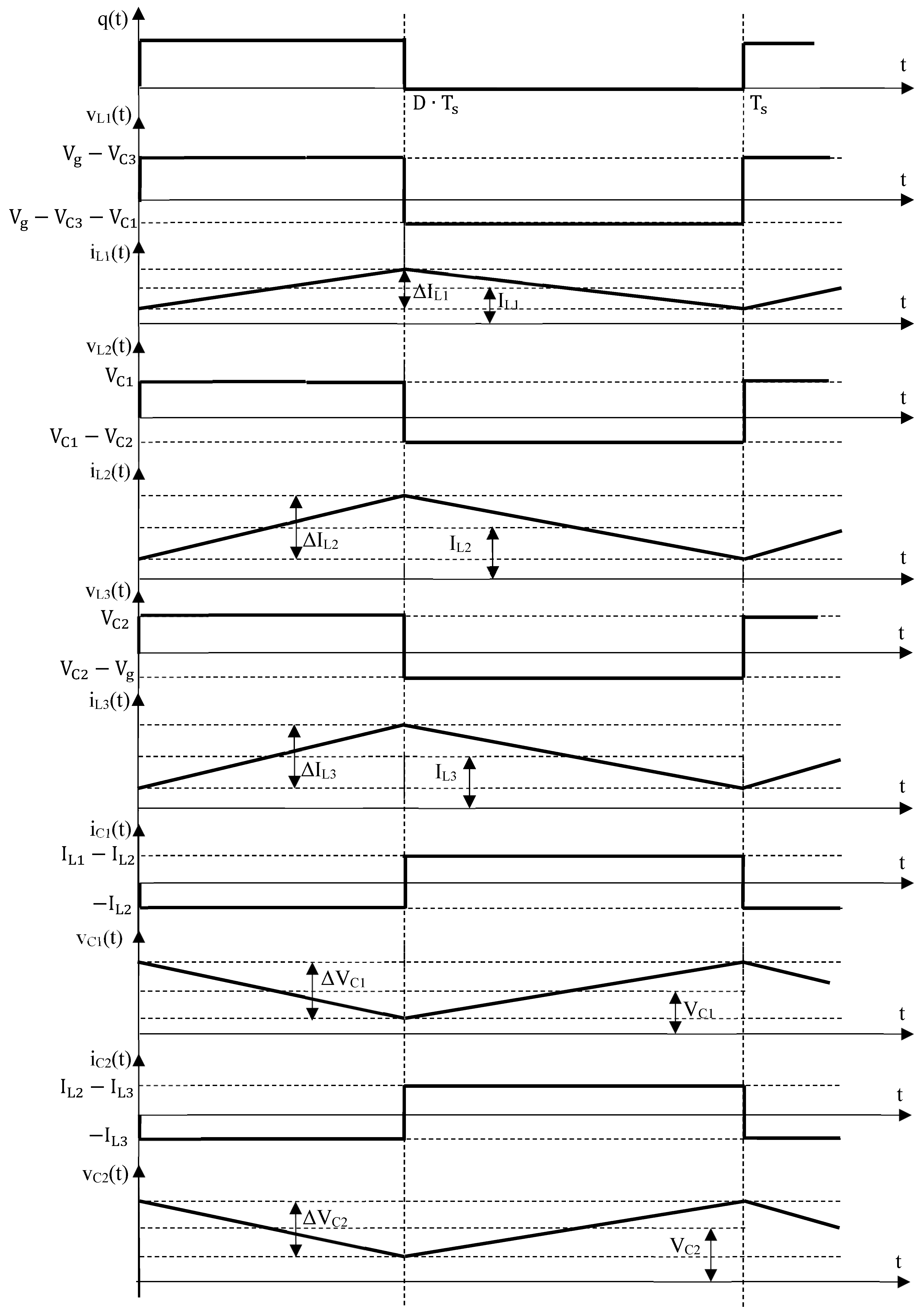
The theoretical waveforms corresponding to the reactive elements are depicted in Figure 5.
In a dc–dc converter design process, in order to be able to choose the suitable devices, a key-role is played by the semiconductor stresses. The voltage stress is given by the topological state in which the respective device is in the off-state, whereas the dc current stress is obtained from its on-state. The final values of the semiconductor stresses result from (7) to (9) and (12) to (14) as:
V S = V g
I S = D · ( I L 1 + I L 2 + I L 3 ) = D 2 · ( D 2 3 · D + 3 ) 2 · V g R = P o V g
V D 1 = V C 1 + V g = D · ( 2 D ) · V g = V g · ( 1 ( 1 M ) 2 3 )
I D 1 = D · I L 1 = D 2 · ( D 2 3 · D + 3 ) · V g R = P o V o · ( 1 1 M 3 )  
V D 2 = V C 1 = ( 1 D ) 2 · V g = V g · ( 1 M ) 2 3
I D 2 = ( 1 D ) · I L 1 = D · ( 1 D ) · ( D 2 3 · D + 3 ) · V g R = P o V o · 1 M 3
V D 3 = V C 2 + V g = D · V g = V g · ( 1 1 M 3 )  
I D 3 = D · I L 2 = D 2 · ( 1 D ) · ( D 2 3 · D + 3 ) · V g R = P o V o · ( 1 1 M 3 ) · 1 M 3
V D 4 = V C 2 = ( 1 D ) · V g = V g · 1 M 3
I D 4 = ( 1 D ) · I L 2 = D · ( 1 D ) 2 · ( D 2 3 · D + 3 ) · V g R = P o V o · ( 1 M ) 2 3
V D 5 = V g
I D 5 = ( 1 D ) · I L 3 = D · ( 1 D ) 3 · ( D 2 3 · D + 3 ) · V g R = P o V o · ( 1 M )  
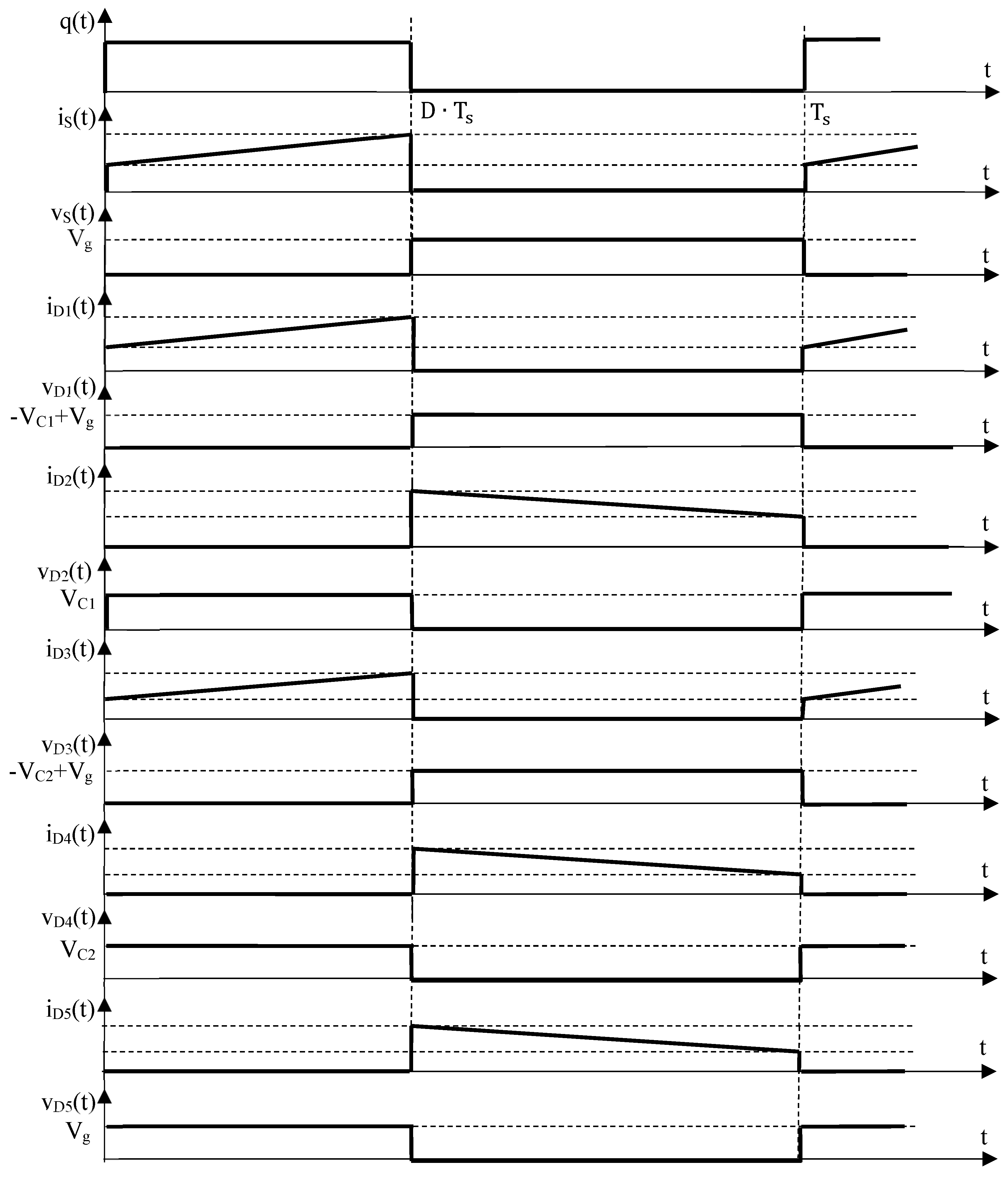
The waveforms associated to the semiconductor devices are sketched in Figure 6, where the voltage stresses are also revealed neglecting the capacitor voltage ripples.
The proposed topology is compared to several other relevant buck-type converters reported in the literature. Table 1 summarizes this comparison revealing the main merit parameters. For a fair comparison, the investigated topologies are all one transistor converters. As expected, as converter order is increasing, the total number of components is increasing too. It can be observed that the proposed topology has the same number of components like the cubic converter in [36] and only one more component compared to the stacked converter reported in [24]. Regarding the number of diodes, the proposed converter is the one with the highest number, together with the cubic [36]. However, in spite of being a cubic topology, the system order is not the highest one, as the stacked [24] is of eighth order. If the static conversion ratio is under discussion, Figure 4 reveals that the proposed converter provides the highest static conversion ratio of all converters at the same duty ratio in the usual duty cycle range.
Transistor dc current stress is very good, as it is lower than the classical [1], cubic [36], quadratic [20] and semi-quadratic [19] and the same as the QBC3 [25]. A comparison to the stacked [24] is irrelevant, as n denotes the number of stages which is an additional parameter that is not present in the other topologies. It can be then concluded that the proposed cubic converter assures the lowest current stress of the transistor. Transistor voltage stress is the same to the classical [1], QBC3 [25], but lower than cubic [36], and quadratic [20] and only the stacked [24], single switch [26] and semi-quadratic [19] operate with a better transistor voltage stress. Hence it can be stated that transistor voltage stress is moderate and better than the cubic [36] counterpart. The same considerations hold for the diode dc current stress that is superior to the cubic [36], stacked [24], QBC3 [25], quadratic [20] and semi-quadratic [19]. Regarding the maximum diode voltage stress, it is equal to the classical [1], QBC3 [25], quadratic [20], higher than semi-quadratic [19], single switch [26] and lower than the cubic [36]. It can be observed that all the merit parameters of the proposed converter are better than the cubic [36], which is an important feature.
As it is known, the conduction losses could significantly modify and influence the static characteristics, including converter efficiency. Therefore, a dc analysis in the presence of losses is compulsory. As the classical dc analysis techniques are difficult to apply in the presence of the losses, the state-space approach is used. The schematic including the conduction losses is presented in Figure 7. The loss elements are the transistor on resistance, Ron, the output capacitor equivalent series resistance RC and the forward voltage diodes drops VD1, VD2, VD3, VD4 and VD5.
The state vector, x, includes the capacitor voltages and the inductor currents. The output vector, y, contains the output voltage, while the input vector, u, consists of the input voltage and the forward voltage drops of the diodes. With these definitions, the resulting state matrices are:
A 1 = R on L 1 R on L 1 R on L 1 0 0 R R + R C · L 1 R on L 2 R on L 2 R on L 2 1 L 2 0 0 R on L 3 R on L 3 R on L 3 0 1 L 3 0 0 1 C 1 0 0 0 0 0 0 1 C 2 0 0 0 1 C 3 0 0 0 0 1 R + R C · C 3 ,       B 1 = 1 L 1 1 L 1 0 0 0 0 0 0 0 1 L 2 0 0 0 0 0 0 0 0 0 0 0 0 0 0 0 0 0 0 0 0 0 0 0 0 0 0 , E 1 = 0 0 0 0 0 R R + R C , F 1 = 0 0 0 0 0 0
A 2 = 0 0 0 1 L 1 0 R R + R C · L 1 0 0 0 1 L 2 1 L 2 0 0 0 0 0 1 L 3 0 1 C 1 1 C 1 0 0 0 0 0 1 C 2 1 C 2 0 0 0 1 C 3 0 0 0 0 1 R + R C · C 3 ,       B 2 = 1 L 1 0 1 L 1 0 0 0 0 0 0 0 1 L 2 0 1 L 3 0 0 0 0 1 L 3 0 0 0 0 0 0 0 0 0 0 0 0 0 0 0 0 0 0 , E 2 = 0 0 0 0 0 R R + R C , F 2 = 0 0 0 0 0 0
The static conversion ratio of the proposed cubic buck-boost converter is obtained as:
M = FD ED · AD 1 · BD
where:
AD = D · A 1 + ( 1 D ) · A 2
BD = D · B 1 + ( 1 D ) · B 2
ED = D · E 1 + ( 1 D ) · E 2
FD = D · F 1 + ( 1 D ) · F 2
If Equation (29) is evaluated with zero lossy elements, the value of the static conversion ratio is the same as in (10), confirming the validity of the ideal static conversion ratio value. Also, the converter efficiency can be calculated using the state-space approach simply by including the input current in the output vector. Moreover, individual component losses can be found extending the output vector with the diode currents and using the dc inductor currents calculated in the state vector.
To ensure a proper converter design, the ripples of the inductor currents and capacitor voltages are necessary. Equations (7)–(9) and (12)–(14) are used for their calculation in the ideal case and the final results are:
Δ I L 1 = D ( V g V C 3 ) L 1 f S = D ( 1 D ) 3 · V g L 1 f S
Δ I L 2 = D V C 1 L 2 f S = D ( 1 D ) 2 · V g L 2 f S
Δ I L 3 = D V C 2 L 3 f S = D ( 1 D ) · V g L 3 f S
Δ V C 1 = ( 1 D ) ( I L 1 I L 2 ) C 1 f S = D 2 · ( 1 D ) · ( D 2 3 · D + 3 ) V g C 1 R f S
Δ V C 2 = ( 1 D ) ( I L 2 I L 3 ) C 2 f S = D 2 · ( 1 D ) 2 · ( D 2 3 · D + 3 ) V g C 2 R f S
Δ V C 3 = Δ I L 1 8 · C 3 f S = D · ( D 2 3 · D + 3 ) V g 32 · C 3 R f S
In order to be sure that the converter operates in CCM, the minimum value of the current through each diode needs to be positive when it conducts. Hence, the imposed conditions for the CCM operation result as follows:
diodes   D 1 , D 2 : 2 · L 1 f S R ( 1 D ) 3 D 2 3 · D + 3
diodes   D 3 , D 4 : 2 · L 2 f S R 1 D D 2 3 · D + 3
diode   D 5 : 2 · L 3 f S R 1 ( 1 D ) · ( D 2 3 · D + 3 )
The reactive elements design is based on fulfilling the small ripple conditions. In case of inductor currents, the ripple is limited to a maximum of 25% of the respective dc current value. For the internal capacitor voltages, the ripples are restricted to being lower than 10% of the dc voltage, while the ripple of the output capacitor voltage is set to a maximum limit of 5% of its corresponding dc value. Taking into account these considerations, from (7) to (9), (12) to (14) and (34) to (39), the minimum values of the reactive components are:
L 1 4 R ( 1 D ) 3 ( D 2 3 · D + 3 ) f S
L 2 4 · R · ( 1 D ) ( D 2 3 · D + 3 ) f S
L 3 4 · R ( 1 D ) · ( D 2 3 · D + 3 ) f S
C 1 10 D 2 ( D 2 3 · D + 3 ) R f S · ( 1 D )
C 2 10 D 2 · ( 1 D ) ( D 2 3 · D + 3 ) R f S  
C 3 5 8 · R f S
In the above equations, the duty cycle is known from the static conversion ratio.
Design example of the proposed cubic buck converter:
  • Input voltage: Vg = 15 V;
  • Output voltage: Vo = 12 V;
  • Output power: Po = 10 W;
  • Switching frequency: fs = 100 kHz.
These design parameters are allowing the immediate calculation of the output resistor and static conversion ratio values, resulting in R = 14.4 Ω and M = 0.8. Afterwards, from (10), a duty cycle of D = 0.4151 is obtained.
The minimum inductor values that assure CCM operation result from (40) to (42) as L1min = 3.26 μH, L2min = 9.53 μH and L3min = 27.86 μH. However, the adopted values of the reactive elements are based on the small ripple assumption, which in case of inductors, is a stronger condition. They are those in (43)–(48), and the final values that are used in the simulation and experimental parts were selected as follows: L1 = 100 μH, L2 = 220 μH, L3 = 820 μH, C1 = 10 μF, C2 = 2.2 μF and C3 = 3.3 μF. Also, the semiconductor devices are chosen after evaluating the stresses described in Equations (15)–(26), which result in IS = 0.6665 A, ID1 = 0.3459 A, ID2 = 0.4874 A, ID3 = 0.2023 A, ID4 = 0.2851 A, ID5 = 0.1667 A, VS = VD5 = 15 V, VD1 = 9.8684 V, VD2 = 5.1316 V, VD3 = 6.2265 V and VD4 = 8.7735 V.
According to these values, the selected devices are specified in Section 3.2.

3. Results

3.1. Simulation Results

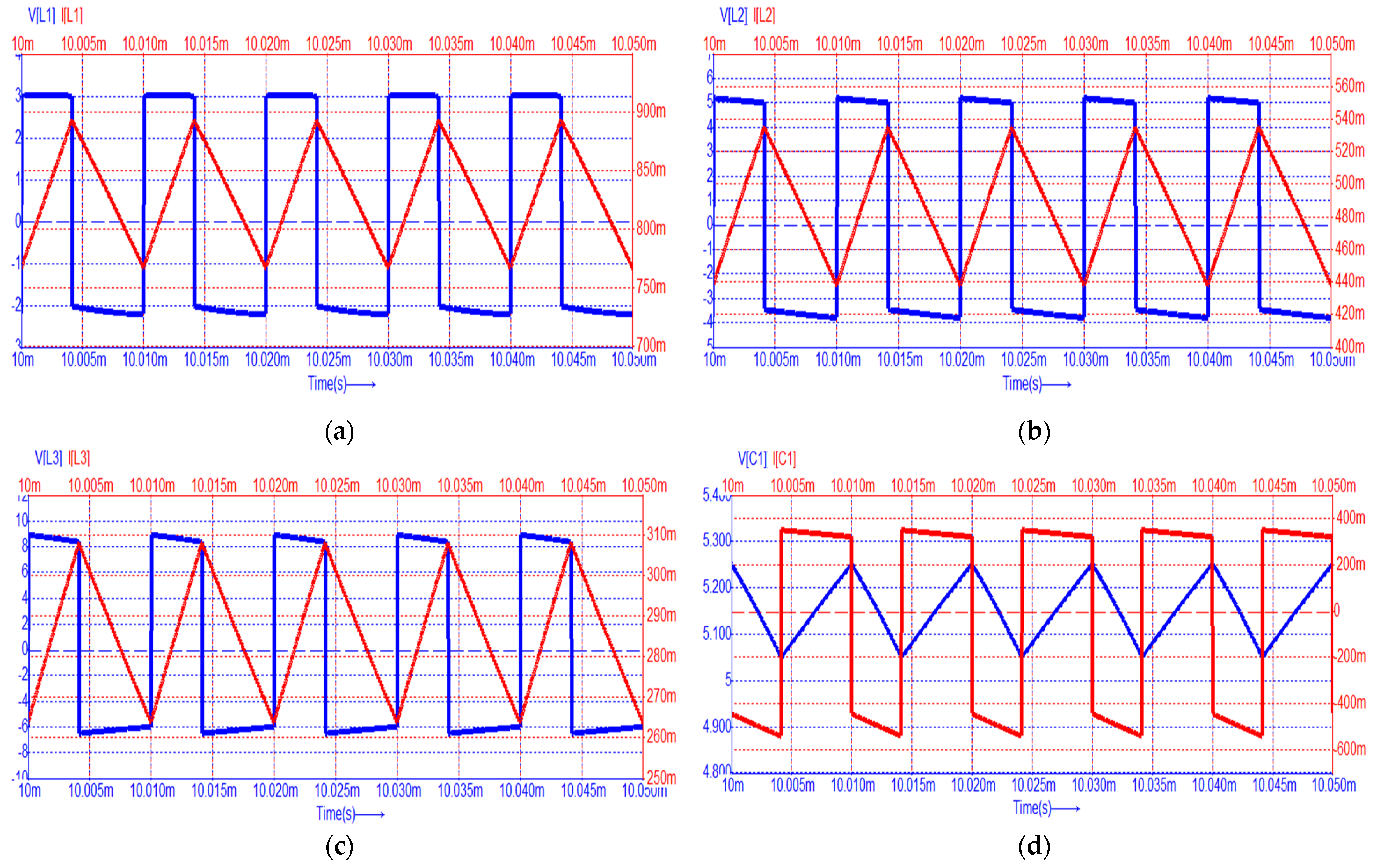
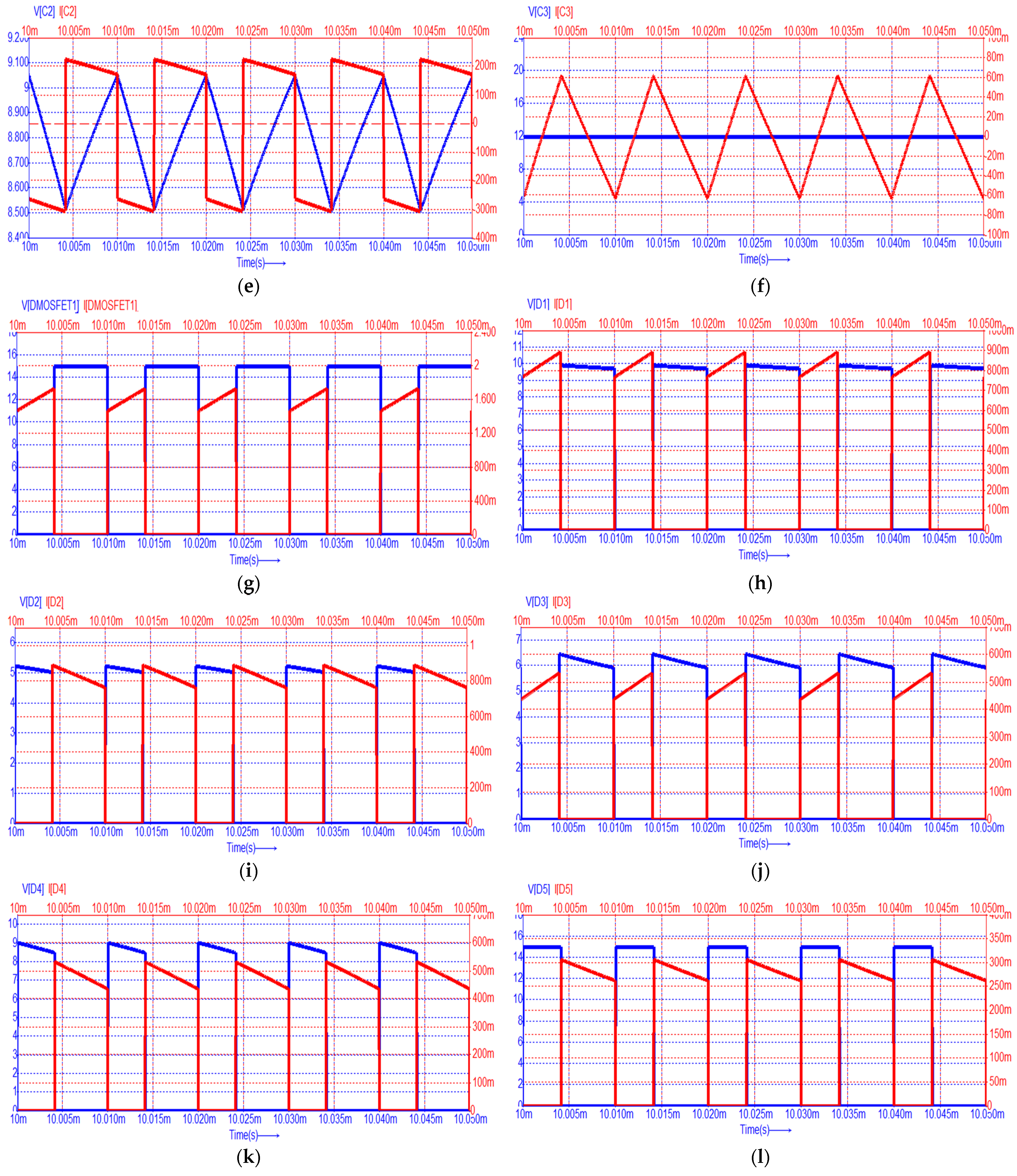
For a first validation of the theoretical considerations, the operation of the proposed cubic buck converter was simulated using the Caspoc [40] simulation tool. All components are assumed to be ideal, with the values that were obtained from the design example. The results are shown in Figure 8, where the current through each device is drawn in red and the voltage across it in blue.
Inspecting the simulation results showed above, it can be observed that the inductor voltages exhibit a rectangular shape, while their currents are triangular, as expected. Quantitatively speaking, the dc values, the peak-to-peak ripples for the inductor currents and the capacitor voltages match to those theoretically predicted, as Figure 5 and Figure 6 reveal compared to Equations (7)–(9) and (12)–(26). The same agreement stands for the dc semiconductor currents and their voltage stresses. Overall, the ideal operation of the proposed converter is validated, and this allows for the next step of experimental validation.

3.2. Experimental Results

For the experimental validation, a prototype of the proposed cubic buck converter was built using the IRLB8721 transistor and the RFN10NS6S diode for all diodes in the circuit. Afterwards, because of its floating connection, the transistor was controlled by a circuit that involved the usage of an optocoupler device.
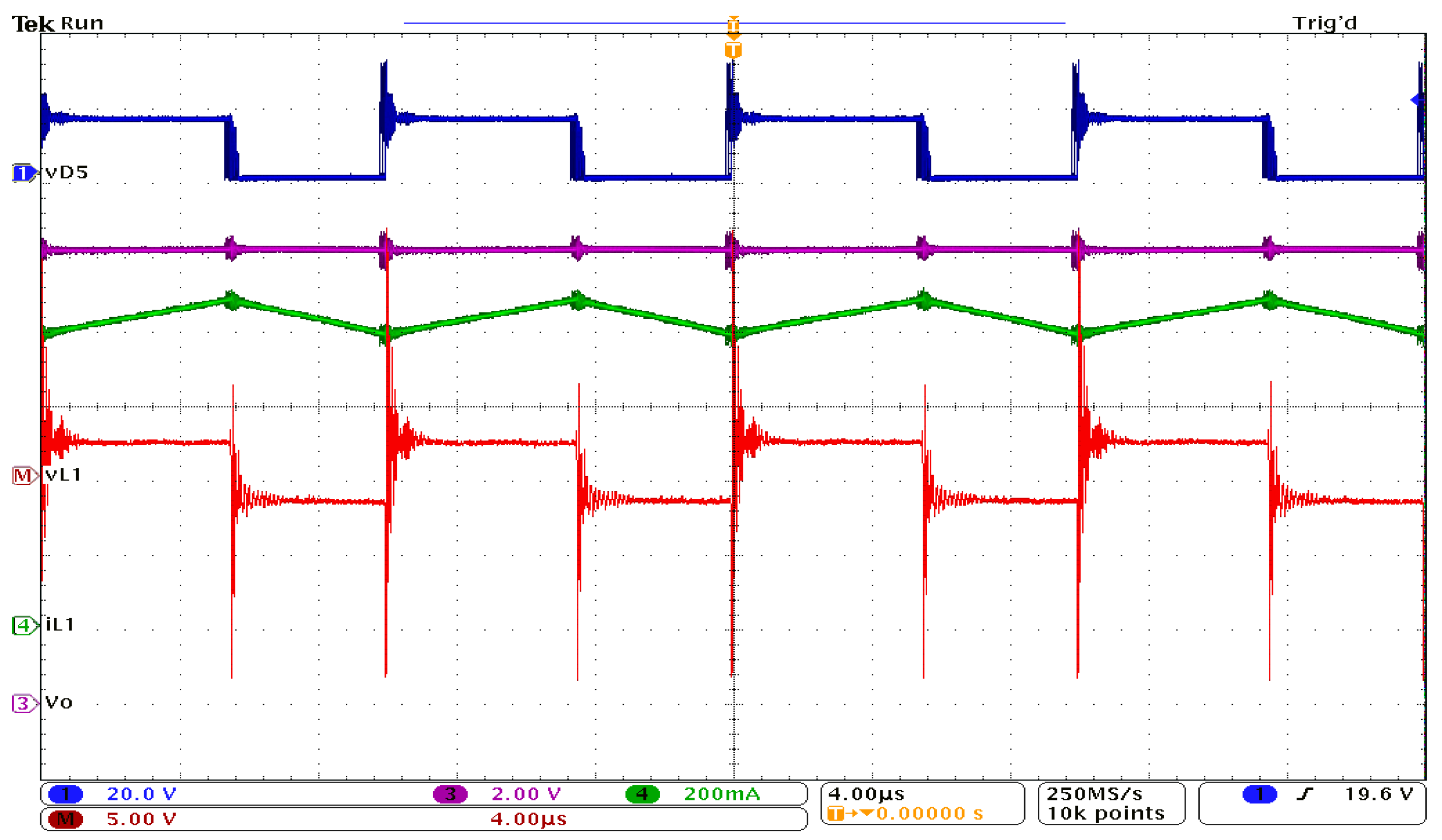
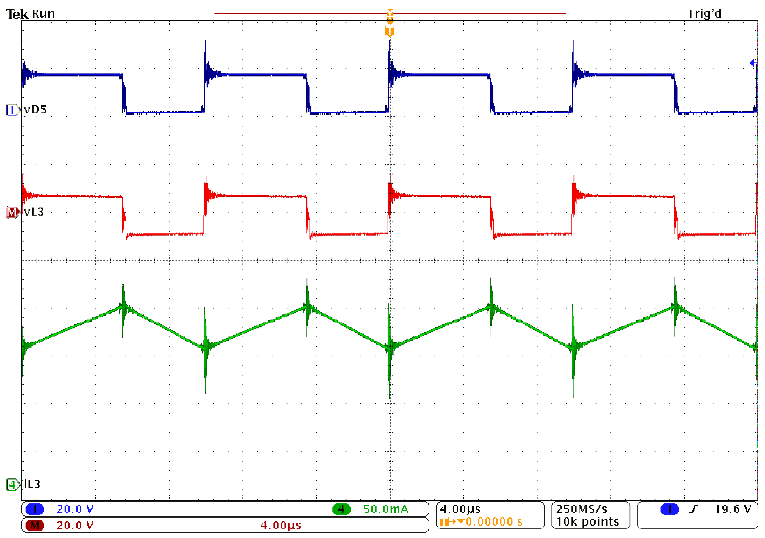
Figure 9 presents the waveforms obtained for the inductor L1 and the output voltage. Figure 10 shows the experimental results for inductor L2, while Figure 11 depicts the current and voltage waveforms for inductor L3. In all cases, the voltage across diode D5 is used as a reference signal. All these waveforms qualitatively confirm the theoretical and simulation results. The spikes accompanying the voltage measurements are due to the fact that a breadboard was used, and the printed circuit board (PCB) was not optimized, as the purpose was to experimentally sustain the feasibility of the proposed topology.
Two cases have been examined with the help of an electronic load operated either as a constant resistor or as a variable resistor.
  • Case 1: different values of the duty cycle and constant output resistor value;
  • Case 2: different resistor values while keeping a constant output voltage.
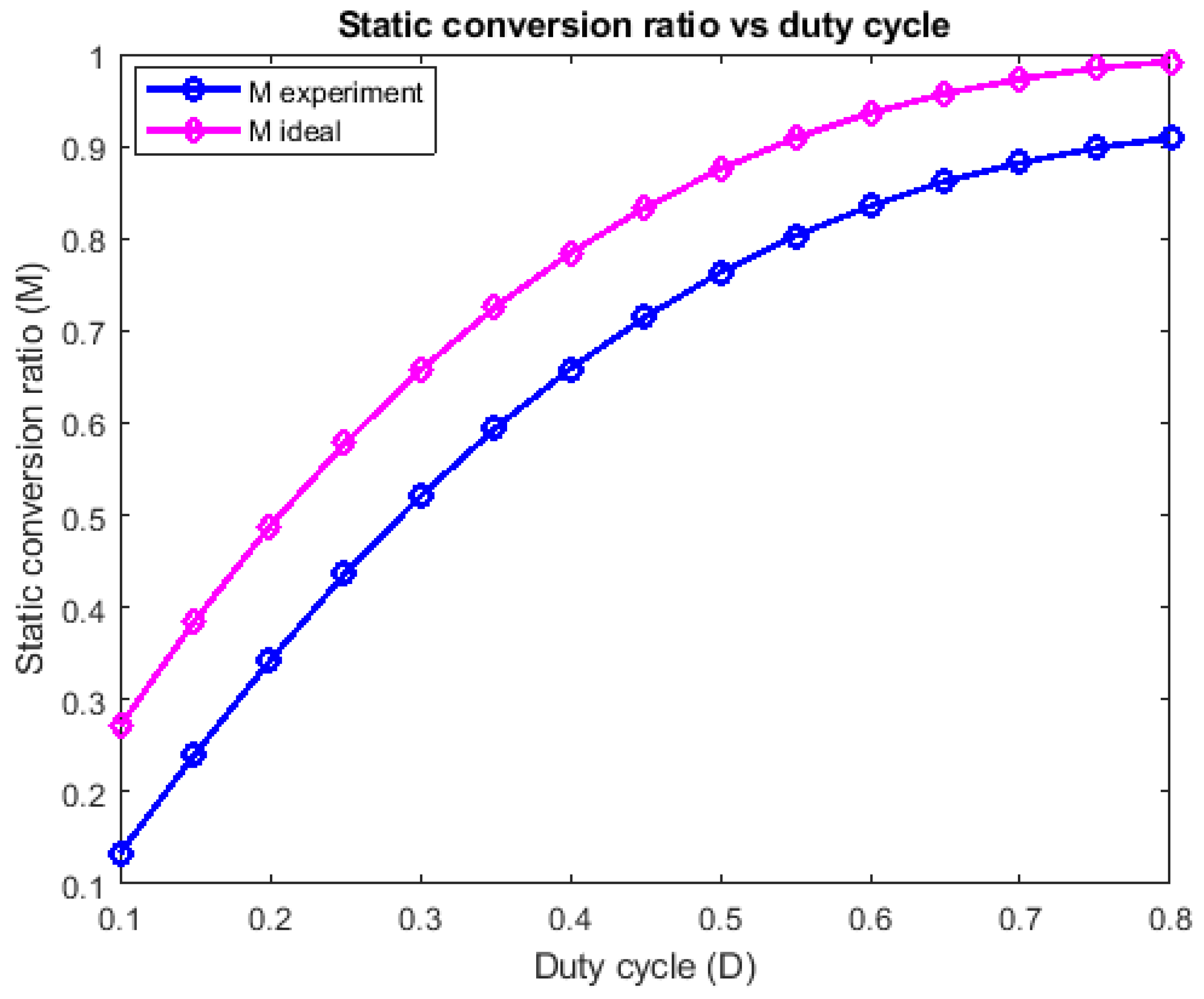
In case 1, the measurements were conducted in order to derive a graphical representation for comparing the ideal and experimental static conversion ratios, results which are shown in Figure 12. In case 2, the experimental efficiency dependency on the output power was studied and it can be seen in Figure 13.
With respect to Figure 12, the measured characteristic exhibits the same shape as the ideal one, but it is shifted downwards. This shift is due to the non-zero voltage drop of the five diodes, their influence being more significant than that of the transistor on resistance. As Figure 13 reveals, the efficiency achieves high values at moderate output power and its flat allure is due to the fact that the number of conducting devices in each topological state is the same (one transistor and two diodes in the first one and three diodes in the second one). As the duty cycle increases, the conduction time of the transistor increases too and also all inductor currents. As a consequence, the power dissipation across the transistor increases, becoming the main power loss, while the total power dissipated by the diodes remains somehow constant, because two diodes are conducting in the first topological state and three in the second one, which is becoming shorter at higher duty cycles. This qualitatively explains why the efficiency is slightly getting lower for high duty cycles. Regardless, the efficiency exceeds 85% on the investigated power range with a small variation with respect to the output power, as seen in Figure 13.

4. Discussion

The paper proposes a single-transistor cubic buck topology. After comparing its operation to a set of seven buck-type converters, it is concluded that, at the same duty cycle, the proposed converter exhibits the highest static conversion ratio; hence, it provides the highest output voltage for the same supply and control. This means that the proposed topology is able to provide a small step-down at moderate duty cycles. Therefore, its practical use will refer to applications in which an output voltage lower, but still close to the input voltage is needed. Such possible applications could be in automotive industry or in renewable energy appliances.
Regarding the transistor current stress, it is the lowest from the set of converters that were analyzed, and all the merit parameters are superior to the known cubic topology. As expected, in the real lossy converter the static conversion ratio is lower compared to the ideal case, but in spite of the fact that five diodes are present, the efficiency is maintained higher than 85% in a reasonable power range.
The CCM operation conditions are derived, together with the peak-to-peak ripples for the inductor currents and capacitor voltages. Using them, a set of equations for designing the inductors and the capacitors are provided. Also, the semiconductor components are chosen based on the device current and voltage stresses.
Simulation and practical experiments confirm all the theoretical considerations with respect to dc analysis, ac analysis, waveforms and design equations.

5. Conclusions

In general, higher order converters proposed in the literature have been limited to quadratic converters, while cubic static conversion ratios are rarely encountered. This paper tries to overpass this barrier and proposes a cubic buck topology that exhibits a higher static conversion ratio than that of the classical buck [1], cubic buck [36], stacked buck [24], QBC3 [25], the quadratic buck [20], single-switch buck [26] and the semi-quadratic buck [19] converters, at the same duty cycle. Compared to the other previously reported cubic topology, the new converter has the same complexity, while exhibiting lower transistor and diodes stresses. In spite of its cubic nature, for a certain application, the duty cycle can be easily determined together with component stresses and high efficiencies are obtained in the investigated power range.
Future research will focus on deriving and analyzing other cubic topologies and exploit their facilities in different applications.

Author Contributions

Conceptualization, D.-A.B., I.-M.P.-C. and D.L.; methodology, D.-A.B., I.-M.P.-C. and D.L.; software, D.-A.B.; validation, D.-A.B. and I.-M.P.-C.; formal analysis, D.-A.B. and D.L.; investigation, D.-A.B. and I.-M.P.-C.; data curation, D.-A.B., I.-M.P.-C. and D.L.; writing—original draft preparation, D.-A.B. and I.-M.P.-C.; writing—review and editing, D.-A.B., I.-M.P.-C. and D.L.; supervision, D.L. All authors have read and agreed to the published version of the manuscript.

Funding

This research received no external funding.

Institutional Review Board Statement

Not applicable.

Informed Consent Statement

Not applicable.

Data Availability Statement

Data are contained within the article.

Conflicts of Interest

The authors declare no conflicts of interest.

References

  1. Erickson, R.W.; Maksimovic, D. Fundamentals of Power Electronics, 2nd ed.; Springer: New York, NY, USA, 2012. [Google Scholar]
  2. Nayak, G.; Nath, S. Voltage Mode Control of Magnetically Coupled SIDO Buck Converter. In Proceedings of the 2018 IEEE International Conference on Power Electronics, Drives and Energy Systems (PEDES), Chennai, India, 18–21 December 2018; pp. 1–6. [Google Scholar] [CrossRef]
  3. Rehman, H.U. Modified Switched-Inductor Based DC-DC Buck-Boost Converter for Low-Power Applications. In Proceedings of the IECON 2021—47th Annual Conference of the IEEE Industrial Electronics Society, Toronto, ON, Canada, 13–16 October 2021; pp. 1–6. [Google Scholar] [CrossRef]
  4. Serra, F.M.; Magaldi, G.L.; Gil-González, W.; Montoya, O. Passivity–Based PI Controller of a Buck Converter for Output Voltage Regulation. In Proceedings of the 2020 IEEE ANDESCON, Quito, Ecuador, 13–16 October 2020; pp. 1–6. [Google Scholar] [CrossRef]
  5. Zhou, X.; Su, D.; Ma, Y.; Pan, J. Research on Auto Disturbance Rejection Control Strategy of Battery Energy Storage Staggered Parallel Buck Converter. In Proceedings of the 2021 IEEE International Conference on Mechatronics and Automation (ICMA), Takamatsu, Japan, 8–11 August 2021; pp. 414–419. [Google Scholar] [CrossRef]
  6. Li, Z.; Xue, Z.; Liang, C.; Zhang, Y.; Duan, M.; Zhao, S.; Liu, X.; Guo, Z.; Geng, L. A Single-input Dual-output Three-level Buck Converter for SoC Applications. In Proceedings of the 2022 IEEE International Conference on Integrated Circuits, Technologies and Applications (ICTA), Xi’an, China, 28–30 October 2022; pp. 127–128. [Google Scholar] [CrossRef]
  7. Tsang, H.K.T.; Fong, Y.C.; Kan, K.L.J.; Raman, S.R.; Cheng, K.W.E. A Study of LLC Converter with Buck Converter for CC-CV Charging. In Proceedings of the 2020 8th International Conference on Power Electronics Systems and Applications (PESA), Hong Kong, China, 7–10 December 2020; pp. 1–5. [Google Scholar] [CrossRef]
  8. Liu, Y.; Kumar, A.; Maksimovic, D.; Afridi, K.K. A High-Power-Density High-Efficiency Three-Level Buck Converter for Cellphone Battery Charging Applications. In Proceedings of the 2018 IEEE Energy Conversion Congress and Exposition (ECCE), Portland, OR, USA, 23–27 September 2018; pp. 5265–5270. [Google Scholar] [CrossRef]
  9. El Kattel, M.B.; Mayer, R.; Possamai, M.D.; Oliveira, S.V.G. A Simplified Analysis of Buck-Type Interleaved DC-DC Converter for Battery Chargers Application. In Proceedings of the 2019 IEEE 15th Brazilian Power Electronics Conference and 5th IEEE Southern Power Electronics Conference (COBEP/SPEC), Santos, Brazil, 1–4 December 2019; pp. 1–6. [Google Scholar] [CrossRef]
  10. Zanatta, N.; Caldognetto, T.; Biadene, D.; Spiazzi, G.; Mattavelli, P. A Two-Stage Twin-Bus Buck Converter for Battery Charging Applications. In Proceedings of the 2023 IEEE Applied Power Electronics Conference and Exposition (APEC), Orlando, FL, USA, 19–23 March 2023; pp. 1908–1914. [Google Scholar] [CrossRef]
  11. Hossain, M.K.; Islam, M.R. Power Stage Design of a Synchronous Buck Converter for Battery Charger Application. In Proceedings of the 2018 International Conference on Advancement in Electrical and Electronic Engineering (ICAEEE), Gazipur, Bangladesh, 22–24 November 2018; pp. 1–4. [Google Scholar] [CrossRef]
  12. Sharma, H.; Sharma, M.; Sharma, C.; Haque, A.; Jaffery, Z.A. Performance Analysis of Solar Powered DC-DC Buck Converter for Energy Harvesting IoT Nodes. In Proceedings of the 2018 3rd International Innovative Applications of Computational Intelligence on Power, Energy and Controls with their Impact on Humanity (CIPECH), Ghaziabad, India, 1–2 November 2018; pp. 26–29. [Google Scholar] [CrossRef]
  13. Talukder, R.; Sridharan, S.; Kapat, S. Performance and Stability Analysis of a Multiphase Buck Converter under Mixed-Signal Current Mode Control for Mobile and Automotive Applications. In Proceedings of the 2022 IEEE 1st Industrial Electronics Society Annual On-Line Conference (ONCON), Kharagpur, India, 9–11 December 2022; pp. 1–6. [Google Scholar] [CrossRef]
  14. Deekshitha, C.; Shenoy, K.L. Design and simulation of synchronous buck converter for LED application. In Proceedings of the 2017 2nd IEEE International Conference on Recent Trends in Electronics, Information & Communication Technology (RTEICT), Bangalore, India, 19–20 May 2017; pp. 142–146. [Google Scholar] [CrossRef]
  15. Widjonarko; Rahardi, G.A.; Avian, C.; Hadi, W.; Herdiyanto, D.W.; Satrio, P.L. Driver for LED Lamp with Buck Converter Controlled by PID. In Proceedings of the 2021 International Seminar on Intelligent Technology and Its Applications (ISITIA), Surabaya, Indonesia, 21–22 July 2021; pp. 216–219. [Google Scholar] [CrossRef]
  16. Raj, A.; Arulgandhi, N.; Patha, L.; Bhaskar, D.V. Fuzzy logic based master-slave controller for paralleling DC-DC converters in LED applications. In Proceedings of the 2018 International Conference on Power Energy, Environment and Intelligent Control (PEEIC), Greater Noida, India, 13–14 April 2018; pp. 676–682. [Google Scholar] [CrossRef]
  17. MMalik, S.; Khan, H.A.; Zaffar, N.A. Evaluation of a Single Inductor based Single-Input Dual-Output Buck Converter for DC Microgrid Applications. In Proceedings of the 2018 IEEE 7th World Conference on Photovoltaic Energy Conversion (WCPEC) (A Joint Conference of 45th IEEE PVSC, 28th PVSEC & 34th EU PVSEC), Waikoloa, HI, USA, 10–15 June 2018; pp. 0613–0617. [Google Scholar] [CrossRef]
  18. Altuğ, B.A.; Kababiyik, A.; Dincol, E.; Batunlu, C. Buck Converter with Optocoupler Based Switching. In Proceedings of the 2021 8th International Conference on Electrical and Electronics Engineering (ICEEE), Antalya, Turkey, 9–11 April 2021; pp. 184–190. [Google Scholar] [CrossRef]
  19. Veerachary, M.; Misal, S. Single-switch Semi-Quadratic Buck Converter. In Proceedings of the 2020 IEEE International Conference on Power Electronics, Smart Grid and Renewable Energy (PESGRE2020), Cochin, India, 2–4 January 2020; pp. 1–6. [Google Scholar] [CrossRef]
  20. Trakuldit, S.; Tattiwong, K.; Bunlaksananusorn, C. Design and evaluation of a Quadratic Buck Converter. In Proceedings of the 2021 8th International Conference on Power and Energy Systems Engineering (CPESE 2021), Fukuoka, Japan, 10–12 September 2021. [Google Scholar]
  21. Li, G.; Amirabadi, M.; Chen, X.; Lehman, B. The Methodology of Constructing the Quadratic Converters. IEEE J. Emerg. Sel. Top. Power Electron. 2022, 10, 6586–6606. [Google Scholar] [CrossRef]
  22. Esam, H. Ismail. Large step-down DC–DC converters with reduced current stress. Energy Convers. Manag. 2009, 50, 232–239. [Google Scholar]
  23. Uno, M.; Kukita, A. PWM Switched Capacitor Converter with Switched-Capacitor-Inductor Cell for Adjustable High Step-Down Voltage Conversion. IEEE Trans. Power Electron. 2019, 34, 425–437. [Google Scholar] [CrossRef]
  24. Lica, S.; Lie, I.; Wegner, A.N.; Pop-Călimanu, I.M. A Generalized Model for Single-Switch Stacked Step-Down Converters. In Proceedings of the 2020 International Symposium on Electronics and Telecommunications (ISETC), Timisoara, Romania, 5–6 November 2020; pp. 1–4. [Google Scholar] [CrossRef]
  25. Palomo, R.L.; Morales-Saldana, J.A.; Hernandez, E.P. Quadratic Step-Down dc-dc Converters Based on Reduced Redundant Power Processing Approach. IET Power Electron. 2013, 6, 136–145. [Google Scholar] [CrossRef]
  26. Botila, D.-A.; Pop-Calimanu, I.-M.; Lascu, D. A Novel Single Switch Step Down Converter. In Proceedings of the 2021 IEEE 19th International Power Electronics and Motion Control Conference (PEMC), Gliwice, Poland, 25–29 April 2021; pp. 31–38. [Google Scholar] [CrossRef]
  27. Santos, E.C.D. Dual-output dc–dc buck converters with bidirectional and unidirectional characteristics. IET Power Electron. 2013, 6, 999–1009. [Google Scholar] [CrossRef]
  28. Chen, G.; Deng, Y.; Dong, J.; Hu, Y.; Jiang, L.; He, X. Integrated Multiple-Output Synchronous Buck Converter for Electric Vehicle Power Supply. IEEE Trans. Veh. Technol. 2017, 66, 5752–5761. [Google Scholar] [CrossRef]
  29. Yau, Y.T. A Non-Isolated Dual-Output High-Step-Down Converter. In Proceedings of the 2022 IEEE Applied Power Electronics Conference and Exposition (APEC), Houston, TX, USA, 20–24 March 2022; pp. 2029–2033. [Google Scholar] [CrossRef]
  30. Roh, Y.-S.; Moon, Y.-J.; Park, J.; Jeong, M.-G.; Yoo, C. A Multiphase Synchronous Buck Converter with a Fully Integrated Current Balancing Scheme. IEEE Trans. Power Electron. 2015, 30, 5159–5169. [Google Scholar] [CrossRef]
  31. Martinez, W.; Imaoka, J.; Itoh, Y.; Yamamoto, M.; Umetani, K. A novel high step-down interleaved converter with coupled inductor. In Proceedings of the 2015 IEEE International Telecommunications Energy Conference (INTELEC), Osaka, Japan, 18–22 October 2015; pp. 1–6. [Google Scholar] [CrossRef]
  32. Montazerolghaem, R.; Adib, E.; Semiromizadeh, J.; Wheeler, P. Zero-Voltage-Switching High-Step-Down Buck Converter with Continuous Output Current. IEEE Trans. Power Electron. 2023, 38, 12886–12894. [Google Scholar] [CrossRef]
  33. Hafez, A.A.A. Multi-level cascaded DC/DC converters for PV applications. Alex. Eng. J. 2015, 54, 1135–1146. [Google Scholar] [CrossRef]
  34. Nejad, M.L.; Esteki, M.; Heidari, R.; Adib, E. An Improved Cascade Buck Converter for High Step-Down DC-DC Applications. IEEE J. Emerg. Sel. Top. Ind. Electron. 2022, 3, 626–634. [Google Scholar] [CrossRef]
  35. Nayanasiri, D.; Li, Y. Step-Down DC–DC Converters: An Overview and Outlook. Electronics 2022, 11, 1693. [Google Scholar] [CrossRef]
  36. Demian, A.E.; Treviso, C.H.G.; Gallo, C.A.; Tofoli, F.L. Non-isolated DC-DC converters with wide conversion range used to drive high-brightness LEDs. In Proceedings of the 2009 Brazilian Power Electronics Conference, Bonito-Mato Grosso do Sul, Brazil, 27 September–1 October 2009; pp. 598–605. [Google Scholar] [CrossRef]
  37. Botila, D.-A.; Pop-Calimanu, I.-M.; Lascu, D. Cubic Buck-Boost Converter with High Step-Up Capability. In Proceedings of the 2022 International Symposium on Electronics and Telecommunications (ISETC), Timisoara, Romania, 10–11 November 2022; pp. 1–4. [Google Scholar] [CrossRef]
  38. Ahmad, J.; Pervez, I.; Sarwar, A.; Tariq, M.; Fahad, M.; Chakrabortty, R.K.; Ryan, M.J. Performance Analysis and Hardware-in-the-Loop (HIL) Validation of Single Switch High Voltage Gain DC-DC Converters for MPP Tracking in Solar PV System. IEEE Access 2021, 9, 48811–48830. [Google Scholar] [CrossRef]
  39. Lascu, D. Controlled Energy Transfer Using PWM and Resonant Converter. Ph.D. Thesis, Politehnica University Timisoara, Timisoara, Romania, 1998. [Google Scholar]
  40. Simulation Research, Caspoc, User Manual. Available online: https://www.simulationresearch.com (accessed on 1 October 2023).
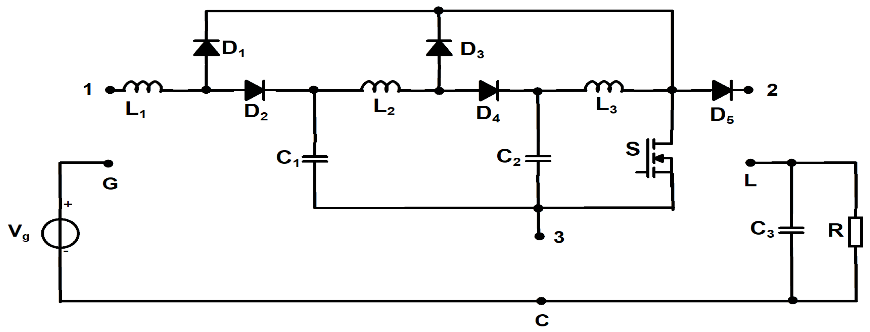
Figure 1. The cubic boost converter from [38]—switching cell extraction.
Sensors 24 00696 g001
Figure 2. The proposed cubic buck topology.
Sensors 24 00696 g002
Figure 3. Topological states of the proposed converter, revealing the conducting devices: (a) first topological state; (b) second topological state.
Sensors 24 00696 g003
Figure 4. Static conversion ratio vs. duty cycle comparison between different buck-type converters and the proposed cubic buck topology: Classical [1](light green); Cubic [36] (dark blue); Stacked, n = 3 [24] (light blue); QBC3 [25] (magenta); Quadratic [20] (red); Single-switch [26] (yellow); Semi-quadratic [19] (black); Proposed (dark green).
Sensors 24 00696 g004
Figure 5. Theoretical waveforms for the reactive elements of the proposed cubic buck converter.
Sensors 24 00696 g005
Figure 6. Theoretical waveforms for the semiconductor devices of the proposed cubic buck converter.
Sensors 24 00696 g006
Figure 7. Proposed cubic buck converter including the lossy elements.
Sensors 24 00696 g007
Figure 8. Simulation results (voltages with blue and currents with red): (a) for inductor L1; (b) for inductor L2; (c) for inductor L3; (d) for capacitor C1; (e) for capacitor C2; (f) for capacitor C3; (g) for transistor S; (h) for diode D1; (i) for diode D2; (j) for diode D3; (k) for diode D4; (l) for diode D5.
Sensors 24 00696 g008aSensors 24 00696 g008b
Figure 9. Experimental waveforms: reference signal, vD5 (dark blue); inductor L1 voltage, vL1 (red); current through L1, iL1 (green); output voltage Vo (purple).
Sensors 24 00696 g009
Figure 10. Experimental waveforms: reference signal, vD5 (dark blue); inductor L2 voltage, vL2 (red); current through L2, iL2 (green).
Sensors 24 00696 g010
Figure 11. Experimental waveforms: reference signal, vD5 (dark blue); inductor L3 voltage, vL3 (red); current through L3, iL3 (green).
Sensors 24 00696 g011
Figure 12. Comparison of the ideal and experimental static conversion ratio against the duty cycle, with constant load resistance.
Sensors 24 00696 g012
Figure 13. Experimental efficiency against output power.
Sensors 24 00696 g013
Table 1. Comparison between the proposed converter and some other step-down topologies.
ParameterClassical [1]Cubic [36]Stacked [24]QBC3 [25]Quadratic [20]Single Switch [26]Semi-Quadratic [19]Proposed
Total no. of
components
413128981113
No. of transistors11111111
No. of diodes15333245
System order26844556
Static Conversion Ratio (M) D D 3 n · D ( 1 + 2 · D ) D · ( 2 D ) D 2 1 2 D D 2 D 1 ( 1 D ) 3
Transistor dc
current stress
P o M · V g P o M · V g 3 · ( n 2 · M ) n · P o M · V g P o V g P o M · V g 2 · ( 2 · M 1 ) · P o M 2 · V g P o M · V g P o V g
Transistor voltage stress V g ( 1 + M 3 + M 2 3 ) · V g n M n · V g V g ( 1 + M ) · V g M · V g 4 · M 2 M + 1 · V g V g
Maximum diode
dc current stress
1 M M · P o M · V g P o M · V g P o M · V g P o M · V g P o M · V g 1 M M · P o M · V g P o M · V g 1 M 3 · P o M · V g
Maximum diode voltage stress V g ( 1 + M 3 ) · V g 2 · M n · V g V g V g M · V g M + 1 2 · V g V g
Disclaimer/Publisher’s Note: The statements, opinions and data contained in all publications are solely those of the individual author(s) and contributor(s) and not of MDPI and/or the editor(s). MDPI and/or the editor(s) disclaim responsibility for any injury to people or property resulting from any ideas, methods, instructions or products referred to in the content.