Article

Compact and Fully Integrated LED Quantum Sensor Based on NV Centers in Diamond

by
Jens Pogorzelski
1,*,
Ludwig Horsthemke
1,
Jonas Homrighausen
2,
Dennis Stiegekötter
1,
Markus Gregor
2 and
Peter Glösekötter
1,*
1
Department of Electrical Engineering and Computer Science, Münster University of Applied Sciences, Stegerwaldstr. 39, D-48565 Steinfurt, Germany
2
Department of Engineering Physics, Münster University of Applied Sciences, Stegerwaldstr. 39, D-48565 Steinfurt, Germany
*
Authors to whom correspondence should be addressed.
Sensors 2024, 24(3), 743; https://doi.org/10.3390/s24030743
Submission received: 21 December 2023 / Revised: 12 January 2024 / Accepted: 22 January 2024 / Published: 24 January 2024
(This article belongs to the Special Issue Quantum Sensors and Quantum Sensing)

Abstract

:
Quantum magnetometry based on optically detected magnetic resonance (ODMR) of nitrogen vacancy centers in diamond nano or microcrystals is a promising technology for sensitive, integrated magnetic-field sensors. Currently, this technology is still cost-intensive and mainly found in research. Here we propose one of the smallest fully integrated quantum sensors to date based on nitrogen vacancy (NV) centers in diamond microcrystals. It is an extremely cost-effective device that integrates a pump light source, photodiode, microwave antenna, filtering and fluorescence detection. Thus, the sensor offers an all-electric interface without the need to adjust or connect optical components. A sensitivity of 28.32 nT / Hz and a theoretical shot noise limited sensitivity of 2.87 nT / Hz is reached. Since only generally available parts were used, the sensor can be easily produced in a small series. The form factor of (6.9 × 3.9 × 15.9) mm 3 combined with the integration level is the smallest fully integrated NV-based sensor proposed so far. With a power consumption of around 0.1 W , this sensor becomes interesting for a wide range of stationary and handheld systems. This development paves the way for the wide usage of quantum magnetometers in non-laboratory environments and technical applications.

1. Introduction

In recent years, negatively charged NV centers in diamond have become established in the field of quantum-based sensing. NV centers can be used to build highly sensitive magnetic field sensors even in the fT / Hz range [1,2,3]. These can be kept extremely small with spatial resolutions down to atomic size [4,5,6,7]. This sensor technology can also measure magnetic fields very accurately combined with low energy and space requirements [8]. NV centers can also be used to measure temperatures [9,10,11,12], electric fields [13] and there are also applications in the field of quantum computing [14,15]. Other magnetic sensing protocols using the NV center include an all-optical approach using spin mixing in the NV ground state [16,17,18] or measurement of the infrared absorption of the infrared transition with near shot-noise limited sensitivity [19]. As they are a solid-state system in diamond, the sensors can be operated at room temperature. Therefore the structure can be kept less complex, as cryogenic temperatures are not required.
The NV center is a point defect in diamond. The diamond crystal structure is shown in Figure 1a. Two of the carbon atoms are replaced by a nitrogen atom (red) and an adjacent vacancy. For an ensemble of NV centers in a solid diamond, all four orientations within the tetrahedral structure of the diamond are possible (indicated by yellow atoms).
A negatively charged NV center is a spin S = 1 system with spin triplets in the ground state ground state ( A 2 3 ) and in the excited state ( E 3 ) (cf. Figure 1b) The optical excitation of the ground state is spin-conserving. The decay of electrons in the m s = 0 spin state leads to fluorescence with a dominant wavelength of 637 nm , while the m s = ± 1 state has a higher probability of non-radiative transitions to the A 1 1 singlet state. Manipulation of the electron spin state with microwave magnetic field resonant to the electron spin transitions in the ground state A 2 3 will therefore decrease the fluorescence emitted by the NV center.
The magnetic sensing capability of the NV center is given by the interaction of an external magnetic field B z (green arrow—cf. Figure 1a) with the electron spin. Due to the Zeeman effect, the m s = ± 1 electron spin states are shifted by the projected parallel component B | | (blue arrow—cf. Figure 1a). This shift can be read out in optically detected magnetic resonance (ODMR) measurements. Without any applied magnetic field, a zero field splitting (ZFS) is still visible due to internal crystal strain. The ZFS center frequency ( D = 2.87 GHz at room temperature) shifts with temperature and is used for temperature sensing [9,20].
For NV ensembles, in which NV centers are aligned along four crystal axes, a sweep of the microwave frequency while observing the fluorescence intensity will yield a total of eight dips in fluorescence, corresponding to the m s = + 1 and m s = 1 levels for each of the four NV quantization axes (cf. Figure 1c).
When examining NV-based sensors a distinction can be made between fiber-based sensors, partial fiber-based sensors and fully integrated sensors. Fiber-based sensors have the pump light source and detection outside the sensor head. Partial fiber-based sensors integrate the pump light source or at least the detection in the sensor head. Fully integrated sensors integrate all optical components and provide an all-electric interface.
The advantage of fiber-based systems is that the sensor head can be made very small [21,22,23]. The laser systems are not limited in their size and performance. Fiber-based systems have the benefit that the light sources which generate passive heat are not installed directly in the sensor head and are therefore not restricted in their size and performance. This makes them ideal for biological applications as they offer more degrees of freedom. In addition, the overall size of the sensor head can be reduced to micrometer diameters [21], which is currently not possible due to the component sizes in integrated sensors. However, the combination of sensitivity and form factor of these sensors have mostly been achieved under laboratory conditions with the aid of additional free beam optics. These optical components are often susceptible to mechanical stress, vibrations and for multimode fibres also fiber bending. Also, optical setups cause high costs and often high additional form factors.
Partial fiber-based sensors integrate the photodiode (PD) and continue to use an external laser [1,24,25,26]. An outstanding form factor with a high integration level in this category is reached by Kim et al. [27] but is currently limited in the reached sensitivity of 32 μ T / Hz . Attempts are also being made to additionally integrate laser diodes as pump light sources inside the sensor head [28,29,30,31] and thus to be fully integrated. However, these devices are relatively large (above 1 cm 3 ), which is partly due to the available size of the laser diodes.
For fully integrated sensors, other pump light sources such as light-emitting diodes (LED) could be a possibility. However, fully integrated LED-based sensors have only been marginally investigated so far [11,32]. The aim of this work is to show that fully integrated sensors enable significantly simpler setups compared to partially integrated sensors or fiber-based systems. This could pave the way for specific industrial applications, especially as they provide an all-electric interface. The aim is not necessarily to compete with the highest sensitivities, but rather to achieve a simple and cost-effective design that still offers good performance. By using an LED, it is possible to reduce both the power consumption compared to a laser and the complexity of the control system. For fully integrated sensors LEDs offer a smaller form factor than laser diodes or similar and are therefore useful as they can reduce the size of the entire sensor head. By using surface mount devices (SMD) and an extremely reduced and modular design, we present a fully integrated LED-based NV magnetometer that reduces the size of the so far smallest fully integrated sensor by Stürner et al. [32] by factor 7 to 0.42 cm 3 . Also, the sensitivity is slightly improved to 28.32 nT / Hz . Major progress in the area of cost savings is achieved by using diamond microcrystals.

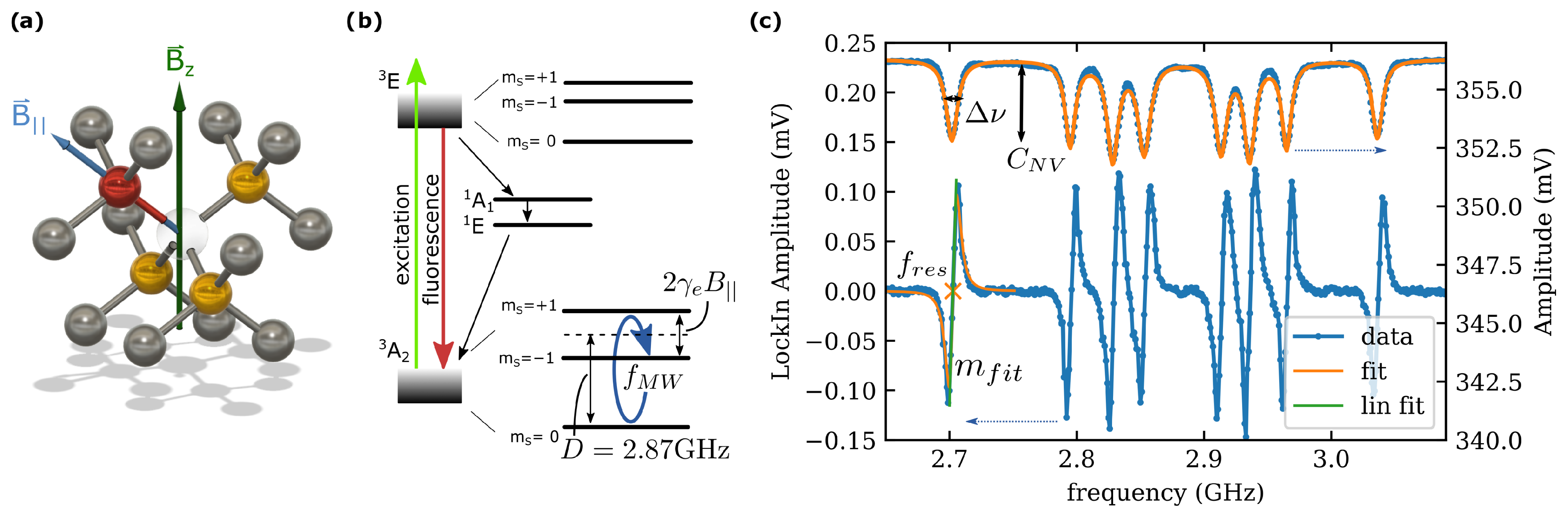
2. Materials and Methods

To build an NV center-based sensor, several key technology components have to be combined: excitation light source, diamond microcrystal, microwave (MW) antenna, red fluorescence filter and photodiode for detection. In a fully integrated sensor, all optical components are included and the sensor has only an electric interface which can be characterized. Difficulties in integration are the interaction between the different signals, heating of the components as well as mechanical stability. The fundamental mechanical sensor structure is described first, followed by a description of the components used.

2.1. Sensor Structure and Mounting

The sensor is designed in a stacked construction as shown in Figure 2a. The main components are three printed circuit boards (PCBs). These can easily be manufactured since standard design rules were used. The first PCB (LED-PCB) has contacts to solder the LED and connect the LED feed line. A 150 μ m sized diamond microcrystal (MDNV150umHi30mg, Adámas Nanotechnologies, Raleigh, NC, USA) is then fixed over the light-emitting chip with an optical adhesive (NOA61, Norland Products, Jamesburg, NJ, USA), onto the epoxy resin that fills the LED housing.
The diamond volume is approximated with a sphere that has a diameter of 170 μ m as the diamonds are slightly larger than specified by the manufacturer. This results in a diamond volume of approximately 0.02 mm 3 . The concentration of NV centers in the diamonds amounts to 2.5–3 ppm [33] which leads to a strong fluorescence signal that can be detected using standard photodiodes. The second PCB provides the MW field and is fabricated as a λ /2 microwave antenna (MW-PCB). The microwave antenna is wrapped around a hole in the MW-PCB, which enables the collection of the fluorescence signal. The photodiode is inserted into the third PCB (PD-PCB). An optical filter (622 nm Longpass Wratten Colour Filter 75 × 75 × 0.1 mmthk, Knight Optics, Harrietsham, Kent, UK) is placed between MW-PCB and PD-PCB. MW-PCB and PD-PCB are both connected via HIROSE U.FL connectors and coaxial cables. The PCBs can be aligned via removable fitting screws. In the final step, the PCBs are fixed with UV adhesive to achieve mechanical stability.

2.2. Microwave Design

The microwave antenna design is based on an omega structure (cf. Figure 2a), whereby the loop of the MW trace leads to a concentration of field strength and an improvement of the field homogeneity around the hole. The length of the antenna is chosen to be exactly half the wavelength of the center frequency of the NV center ground state. This ensures that a minimum of the electric field will be in the center of the resonator length and therefore a maximum of the magnetic field is reached in the hole of the PCB. The resonator length of the PCB trace is calculated as:
λ P C B / 2 = v f · c f M W / 2 = c ϵ r c o r e f M W / 2 = 24.62 mm
where λ P C B is the wavelength of the electromagnetic wave in a copper trace on a PCB, v f = 1 / ϵ r c o r e = 1 / 4.5 is the velocity factor of the core material with ϵ r c o r e = 4.5 given by the PCB manufacturer, c is the speed of light and f M W is the designated resonance frequency, here chosen as f M W = 2.87 GHz . The MW trace is wound around the mechanical hole as well as the manufacturing guidelines allow. Also, the antenna is set up as a coplanar waveguide with a ground plane to reduce electromagnetic coupling into the photodiode traces underneath the ground plane. The calculated length is used for setting up a COMSOL Multiphysics simulation of the antenna geometry of the MW-PCB. The simulation shows the effective field guidance (cf. Figure 2b). Almost the entire field that could interfere with the photodiode is guided into the ground plane (GND). In the diamond area, a uniform field distribution over the whole diamond volume is achieved with a maximum deviation from the z-axis of θ m a x = 2.83 ° and an average deviation θ a v = 1.53 ° where θ is the angle between the magnetic field component in z-direction and the total component of the magnetic field. The calculated values are comparable to widely used geometries of NV center antennas [34,35].

2.3. Optical Components

An indium gallium nitride LED (150224GS73100, Wuerth Elektronik eiSos GmbH & Co. KG, Waldenburg, Germany) with 525 nm dominant wavelength [36] is used as an excitation light source. A directional light output of 1500 mcd is given in the datasheet [36]. The LED is inserted through the PCB and then soldered on the top side so that it is fixed on a flat surface with the underside of the LED PCB. The emission spectra of the LED slightly overlap with the fluorescence spectra of the diamond (Figure 3a) which normally does not appear in laser applications. For LED applications, the filter must be selected appropriately. A 600 nm filter causes residual light from the LED to worsen the signal-to-noise ratio. Consequently, we use a filterfoil with 622 nm cutoff wavelength (622FWP7575, Knight Optics, Harrietsham, Kent, UK). To collect the fluorescence signal a SMD photodiode (VEMD1060X01, Vishay Intertechnology Inc., Malvern, PA, USA) is mounted similarly to the LED through the PCB. The cut-out in the PD-PCB is shifted from the center to place the detector area central underneath the hole of the MW-PCB. This type of mounting allows the alignment and therefore the beam path to be optimized. The holes in the PCB determine the positions of the components. The screws for connecting the PCBs in turn align the PCBs to each other. For the beam path, the assumption is made that the diamond is located about 100 μ m above the hole and acts as a point emitter (Figure 3b). At a maximum angle of α = 43.0 ° , the rays hit the filter and are refracted there. Because reflections are not expected, the transmission from filter to photodiode is considered consistent. With the filter height h f = 100 μ m and the thickness of the epoxy between the top of the photodiode to the sensor area h g = 150 μ m , the result is an area where fluorescence illuminates a detector with a radius r f l of
r f l = r h + t a n ( δ ) · ( h f + h g ) = r h + tan arcsin s i n ( α ) · n a i r n f · ( h f + h g ) = 629.3 μ m
where r h is the hole radius of the MW PCB, h f is the thickness of the filter, h g is the thickness of the glass above the detector area, n f is the refractive index of the filter and n a i r is the refractive index of air. This gives enough room to place the PD PCB and to irradiate the entire detector surface.

2.4. Measurement Setup

To read out fluorescence signals, a customized transimpedance amplifier (TIA) is used described in a previous publication [37]. The TIA output voltage is fed into a lock-in amplifier (LIA) (MFLI, Zurich Instruments, Zurich, Switzerland). The microwave signal is generated by a vector signal generator (SMBV100B, Rhode & Schwarz, Munich, Germany). The LED is driven by a lab-built constant current source (CCS), powered by a 9 V block battery and adjusted to 30 mA output current. Furthermore, a multimeter (GDM9061, GW-Instek, Taipeh, Taiwan) is used to measure the output voltage of the TIA or the temperature with a thermocouple type K. A block diagram is shown in Figure 2c.
To provide a bias magnetic field and impose oscillating fields a pair of Helmholtz coils are used and calibrated with a Hall effect sensor (SS94A2D, Honeywell, Charlotte, NC, USA). The current is provided by a four-quadrant power supply (TOE 7621, Toellner Electronic Instrumente GmbH, Herdecke, Germany) set up as a voltage-controlled current source.The input voltage is provided by a signal generator output of an oscilloscope (RTA4004, Rhode & Schwarz, Munich, Germany).

2.5. Output Signal Model

The presence of an arbitrary magnetic field is assumed. Due to the Zeeman effect, resonances spilled to up to eight resonances as shown in Figure 1c. A fluorescence resonance dip measured as the output voltage of the TIA V T as a function of the frequency f M W can be approximated with a Lorentzian line shape and, therefore, the whole output signal as the summation of eight Lorentzian dips.
V T = V 0 i = 1 8 C N V i 1 + ( 2 ( f M W f r e s i ) / Δ ν i ) 2
where V 0 is the measured voltage in the non-resonant case and f r e s i are the resonance frequencies of the individual dips. Δ ν i is the parameter that characterizes the width of the dip. Here, it is used synonymously with the full width at half maximum (FWHM) of the dips. C N V i are the contrast values of the individual dips.
The resonant frequency of a dip depends on the parallel component of an external magnetic field with respect to the corresponding NV-axis. An arbitrary external magnetic field B a therefore shifts the frequency of the dip by the vectorial component parallel to the NV-axis B | | . To further characterize the output signal, one resonance is considered separately and Equation (3) is written as
V T ( t ) = V 0 C N V 1 + 4 ( f M W γ e B | | ( t ) ) 2 Δ ν 2
where γ e = h / ( g e μ B ) is the gyromagnetic ratio with h as Planck’s constant, g e as the electronic g-factor and μ B as the Bohr magneton.
The microwave frequency f M W can either be swept linearly, kept constant or be amplitude- or frequency-modulated (FM). Besides noise reduction, the use of FM has the advantage that the output signal is the derivative of the resonance spectrum after demodulation of the lock-in technique (cf. Figure 1c). The center frequencies of the resonances can be detected as zero crossings. Here, FM is used and is given by the carrier frequency f c , the frequency of the local oscillator f L F and frequency deviation f d e v i . f L F is used as the demodulation frequency f r e f of the LIA. The FM modulated microwave as function of t is written as
f M W ( t ) = f c + f d e v i · sin ( 2 π f L F t )
V T can therefore be written as
V T ( t ) = V 0 C N V 1 + 4 ( f c + f d e v i sin ( 2 π f L F t ) γ e B | | ( t ) ) 2 Δ ν 2 .
With this equation, the frequency spectrum of specific points of the resonance spectrum can be modeled.
To simulate a realistic working point B a is set to a static component with a one-sided sinusodial offset B a ( t ) = B d c + B ^ a c / 2 ( 1 + sin ( 2 π f B a c t ) ) . With the projected magnetic field components to the NV-axis, the output signal is written as
V T ( t ) = V 0 C N V 1 + 4 ( f c + f d e v i sin ( 2 π f L F t ) γ e B d c | | γ e B ^ a c | | / 2 ( 1 + sin ( 2 π f B a c t ) ) 2 Δ ν 2
A linear spectral density spectrum of the simulated time series is shown in Figure 6. Additional 50 Hz harmonics (due to the European grid frequency) and a Gaussian noise were added to visualize the signal more realistically.

2.6. Measuring of Small Magnetic Field Changes

If V T is an FM-modulated signal and fed into an LIA, the demodulated output signal of the LIA V L I A is an approximation to the derivative of the input signal (cf. Figure 1c). In the immediate vicinity of the resonance f r e s and therefore the zero crossing of V L I A , the demodulated signal of one resonance can be fitted linearly with the slope m f i t . In this range, the magnetic field parallel to one NV-axis is related to the signal output with:
Δ B | | = Δ V L I A γ e · m f i t .
V L I A is the amplitude output voltage multiplied by the sign of the phase Θ of the LIA and m f i t the slope fitted to the demodulated spectrum. If the orientation of the diamond is not known, the applied magnetic field cannot be calculated directly by measuring only Δ B | | . In the measurement setup shown in Figure 1c. B a is limited to the known direction of the z-axis related to a coordinate system given by the direction of the Helmholtz coil. The NV-axis that is mostly parallel to the applied external field can easily be recognized by the largest Zeeman splitting. With a correction factor cos ( θ ) that can be determined by vector projection between B | | and one known magnetic field value of B z , it is then possible to measure Δ B z with only one resonance frequency
Δ B z = Δ B | | / cos ( θ ) = Δ V L I A γ e · m f i t · cos ( θ ) .

3. Results

3.1. Crosstalk between MW-PCB and PD-PCB

With a vector network analyzer (ZNB8, Rhode & Schwarz, Munich, Germany) the transmission factor between the MW connector (port S 1 ) and the photodiode connector (port S 2 ) is measured. The frequency range is set from 2.4 GHz to 3.4 GHz . The S 12 parameter shows a high isolation value of S 12 = 51 dB over the entire used frequency range which proves analog shielding between MW and the photodiode signal.

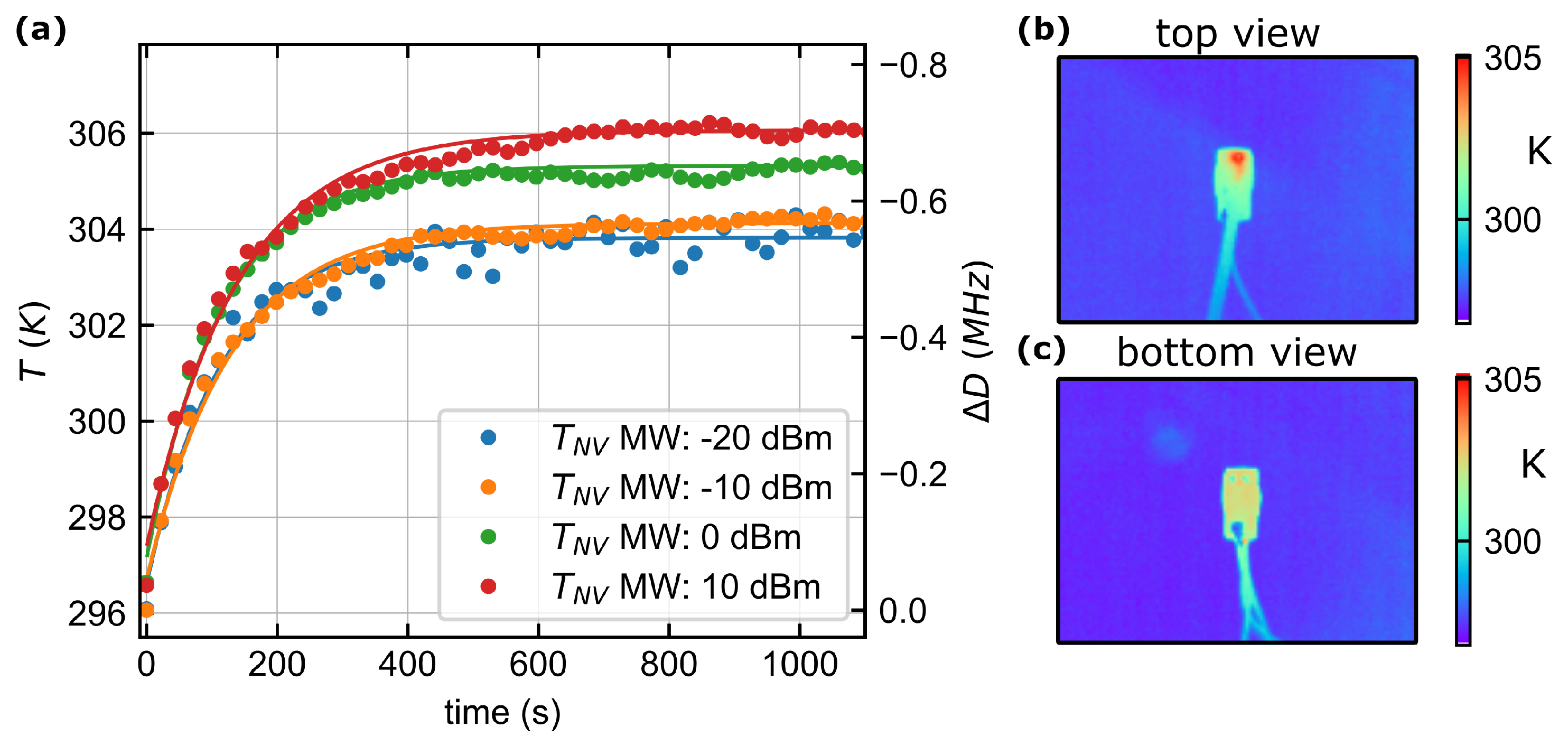
3.2. Thermal Response

The temperature behavior of the sensor is studied. With an FM scan between 2.845 GHz and 2.895 GHz , the zero field splitting without an applied magnetic field is measured. The microwave power is varied between P M W = 20 dBm and P M W = 10 dBm . The shift of the ZFS, which is designated D, is measured. The shift is caused by the increased temperature [9] of the diamond due to the thermal and optical heat radiated by the LED and the heat induced by the microwave. The results are shown in Figure 4a. We observe a maximum shift of the ZFS of Δ D = 703 kHz at P M W = 10 dBm at a constant ambient temperature of 296.2 K ( 23.05 ° C ) . Acosta et al. systematically investigated the behavior of the ZFS in the temperature range 280– 330 K [9] and found an average factor d D / d T = 74.2 kHz / K for various diamonds with different concentrations. The diamond used is comparable to the diamonds used by Acosta due to its NV concentration. The factor is therefore used to determine the temperature shift within the diamond. We estimate a temperature increase of only Δ T N V m a x 9.8 K and a total temperature inside of the sensor of T N V 306 K ( 32.85 ° C ) . The surface temperature of the sensor was measured with a thermal imaging camera (E40, Teledyne FLIR, Wilsonville, OR, USA) directed at both the LED-PCB (cf. Figure 4b) and the PD-PCB (cf. Figure 4c). The ambient temperature for these measurements is 296.9 K ( 23.76 ° C ) . Outside the sensor, a maximum surface temperature of T s f = 305 K ( 31.85 ° C ) can be measured at a contact of the LED. Δ T s f = 8.1 K is slightly lower than the measurements via the ZFS inside the sensor.

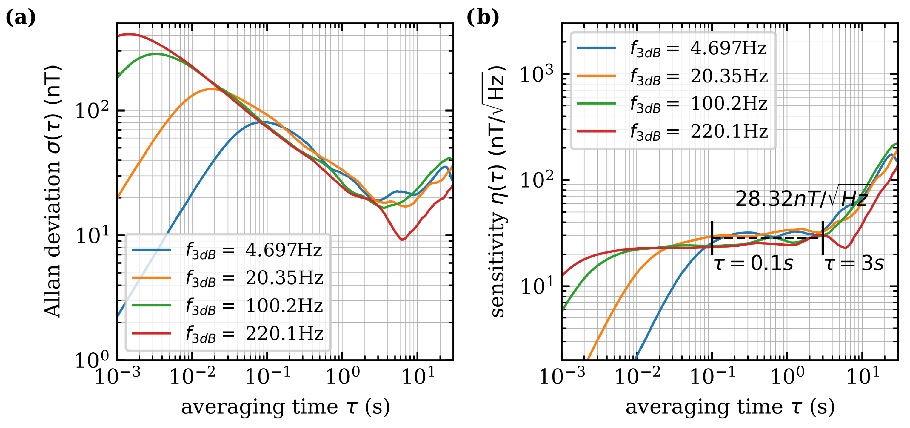
3.3. Shot Noise Limited Sensitivity (SNLS)

To further optimize the sensor performance, the parameters regarding the FM are varied. To compare different working points the shot noise limited sensitivity for a continuous wave (CW) application with a Lorentzian line shape [38,39] is calculated by
η S N L = 4 3 3 γ e Δ ν C N V R
where 4 / 3 3 is a factor regarding the Lorentzian line shape, Δ ν is the full width half maximum (FWHM) of the resonance, C N V is the contrast of a resonance dip and R is the detected photon count rate. R is the photocurrent calculated by the output voltage of the TIA in the non-resonant case V 0 and the feedback resistor of the TIA [1]. To measure a resonance spectrum, an offset magnetic field of B z = 6.1 mT is applied by an external Helmholtz coil. The resulting eight resonances were fitted with several Lorentz functions (Equation (3)) and the values for C N V and Δ ν were determined.
First, the dependence of sensitivity with respect to microwave power P M W is investigated. Therefore the local oscillator frequency f L F is set to 1 kHz and the frequency deviation f d e v i to 3 MHz . The results show an increased contrast but also broadened linewidth of the resonances with increasing microwave power (cf. Figure 5a). Above P M W = 10 dBm , the sensitivity slowly decreases again.
The variation of the local oscillator frequency f L F is performed with P M W = 10 dBm and f d e v i = 2 MHz (cf. Figure 5b). When the 1/f noise is left the LF frequency has no measurable effect in the chosen frequency range. Δ ν and C N V remain nearly constant.
For the last analysis, the frequency deviation f d e v i is swept in the range of 50 kHz and 4 MHz (cf. Figure 5c). Since it was decided to work with microwave power that does not resolve the hyperfine structures of the diamond microcrystals used in CW applications, the most sensitive range differs from other publications [1,40]. The measurements show that to achieve η S N L 3 nT , the parameter set for the FM should be selected from the following: P M W = [ 5 , 10 ] dBm , f d e v i = [ 1.8 , 3 ] MHz and f L F = [ 1.5 , 20 ] kHz .

3.4. Noise Measurement

In order to characterize the sensor further, the noise behavior of the sensor is investigated. The output voltage of the TIA is connected to the scope of the LIA without any external or internal filters and the bandwidth is set to 1 MHz with a Hann window function. The voltage spectral density is measured and shown in Figure 6. The blue spectra are the noise floor without any signal cable. The orange spectra show the output voltage spectral density of the TIA with the connected sensor, the microwave generator running at 10 dBm tuned to non-resonant case of about 2.4 GHz and a magnetic field through the Helmholtz coil of B a ( t ) = 6.11 mT + 25 μ T sin ( 2 π · 225   Hz · t ) . 50 Hz interference of the mains, as well as their harmonics, can be clearly seen here as in all spectra. The LED is then switched on and the microwave is operated off-resonant.
To show the noise behavior at a specific resonance, the carrier frequency f c of the FM microwave is set to resonance at γ e B d c | | following Equation (7). The spectrum is recorded again (green spectra). Figure 6 clearly shows the signal oscillating with the local oscillator frequency f L F = 1.5 kHZ and the sinusoidal component of B a ( t ) with f B a c = 225 Hz signal added as side bands with harmonics which strongly correlate with the calculated purple spectra of Equation (7). Above 28 kHz , interference caused by the TIA can be observed. In the current configuration, f L F is therefore limited to this frequency. According to Howard [41], uncorrelated power density spectra G ( t , f ) can be summed for t as G Z ( f ) = G X ( f ) + G Y ( f ) . Therefore, the noise of the LED can be analyzed in more detail by looking at the difference between the spectral density S E L ( f ) = G E L ( f ) of the electronic without the LED and the spectral density S I ( f ) = G I ( f ) of the insensitive case where the LED is turned on. Leaving the 1 / f regime the average spectral density of the LED in the frequency range 1 kHz < f * < 28 kHz is calculated as
[ S ¯ L E D ( f * ) ] = [ S ¯ I ( f * ) ] 2 [ S ¯ E L ( f * ) ] 2 .
The result is that the spectral density of the LED is by factor 2.4 bigger then the spectral density of the remaining electronics and is therefore the dominant noise source in this case.
Figure 6. Measured voltage spectral density for different cases. Purple spectra: A simulated spectral density according to Equation (7) is shown whereas the amplitude is chosen arbitrarily. Blue spectra: the noise floor measured without any signal cable attached. Orange spectra: all devices running. LED is turned off. Red spectra: The LED is then turned on and the microwave is kept in a non-sensitive regime of 2.4 GHz . Green spectra: the carrier frequency f c of the microwave is tuned to resonance. The frequency peaks follow the simulated frequency comb (purple).
Sensors 24 00743 g006

3.5. Magnetic Sensitivity

The minimum detectable magnetic field and the sensitivity as a function of the integration time are determined using the Allan deviation. Allan deviation is a statistical metric commonly used to evaluate the deviation of measurement data grouped in intervals with an averaging time referred to as τ . Unlike standard deviation, Allan deviation systematically examines data sets with respect to the averaging time τ providing valuable insight into the noise characteristics of the system and the low-frequency drift behavior of the sensor. The Allan variance is calculated as [42]
σ ( τ ) 2 = 1 2 ( y ¯ n + 1 y ¯ n ) 2
where y ¯ n + 1 and y ¯ n are two adjacent mean values sampled over the sample time τ . The brackets denote an infinite time average. To reduce external influences such as magnetic noise induced by the Helmholtz coil, a permanent magnet is used to split the resonances. The microwave is tuned to resonance and demodulated data is recorded for 60 s at a sample rate of 13.39 k / s . The cut-off frequency of the LIA is varied between f 3 d B 5 Hz and f 3 d B 220 Hz . Valid values only arise above the resulting time constant of the filter. The resulting Allan deviation is shown in Figure 7a and the sensitivity in relation to the integration time is shown in Figure 7b. The minimum detectable magnetic field change as an average of the minima of all four curves is Δ B m i n = 15.44 nT . With short integration times τ , white noise dominates, which can be averaged out with longer integration times. The higher the cut-off frequency of the LIA is selected, the lower the absolute measurable field becomes. The mean sensitivity between τ = 0.1 s and τ = 3 s is η = 28.32 nT / Hz . The increase in sensitivity above τ = 2 s shows that low-frequency components dominate at this point. This measurement shows a high sensitivity despite the unshielded environment.

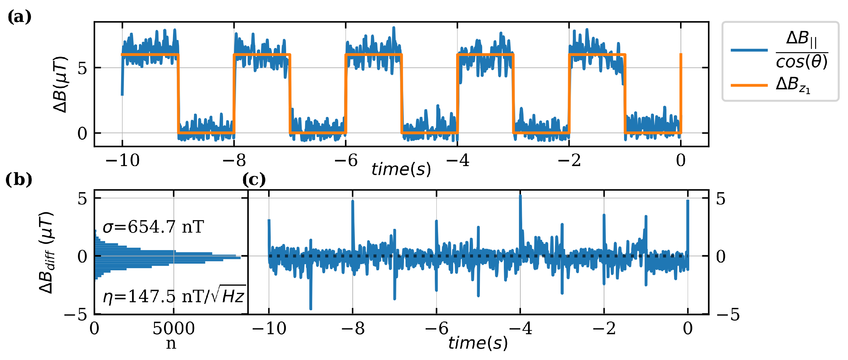
3.6. Practical Application of Magnetic Field Measurement

To further determine the accuracy and precision of the sensor a known magnetic field is measured over time in two time series measurements. Two different magnetic fields are generated by the Helmholtz coil: (1) A square wave signal simulates switching processes. (2) A sinusoidal signal simulates a sinusoidal current.
For both measurements, an alternating component is added to the constant component of the current through the Helmholtz coil to generate a magnetic field B z = B z d c + Δ B z . Since the orientation of the diamond to the magnetic field is not known, a correction factor must be assumed (Equation (9)) and is calculated for both measurements. A known magnetic field offset of B z d c = 6.11 mT is set, and B | | = 5.94 mT is measured for the resonances with the largest shift (cf. Figure 1a). Therefore, the offset angle is calculated as θ 13.6 ° .
For the first measurement, a square wave signal is added to the Helmholtz coil for the measurement time of ten seconds
Δ B z 1 ( t ) = 6   μ T · 1 + sign ( sin ( 2 π · 0.5 Hz · t ) ) 2 .
Measurement and reference are shown in Figure 8a. The difference between Δ B z 1 and the corrected measurement signal is shown in Figure 8c. The histogram of the measured difference between reference and measurement signal is shown in Figure 8b. The standard deviation of σ = 654.7 nT and the resulting sensitivity is η = σ / B W N E P = 147.5 nT / Hz .
The second measurement is performed with a sinusoidal offset as
Δ B z 2 = 30 μ T · ( 1 + sin ( 2 π · 200 Hz · t ) ) .
A reduced period of around 80 ms of the whole measurement time of 2 s is shown in Figure 9a as an example. Due to the higher bandwidth of the filter, the standard deviation is higher whereas the sensitivity with η = 187.44 nT is comparable to the measurement before. However, the measured sensitivity for both measurements differs from previous noise analyses of about factor 6. The main reason for that is visible deviations from the applied magnetic field. The Helmholtz coil is fed by a current source that provides a Δ I C o i l = 1 mA at an offset of I C o i l = 932 mA . The measured current value has a standard deviation of σ c u r r e n t = 0.69 mA which results in a σ B z = 4.35 μ T . In addition, all measurements were performed unshielded in a noisy environment.

4. Discussion

In summary, we have developed a quantum sensor that is easy to build and performs similarly to previously published fully integrated and partly integrated sensors (cf. Figure 10). The use of commercially available components, the stacking of three commercially available PCBs, the use of a randomly orientated diamond microcrystal and the fact that no additional focusing optics are required shows that the sensor is easy to set up. Additionally, it simplifies the overall complexity and also the costs of the whole sensor system by providing an all-electric interface. Besides that, the sensor presented here is the smallest in the range of fully integrated sensors. The reached size of (6.9 × 3.9 × 15.9) mm 3 reduces the overall volume by approx. factor 7 compared to the so far smallest fully integrated sensor by Stuerner et al. [32]. By using a diamond microcrystal, the magnetic field to be measured can be resolved finely by a volume of approx. 0.02 mm 3 . Comparing the cost of one 150 μ m high-pressure high-temperature (HPHT) diamond microcrystal with a 3 × 3 × 0.5 mm 3 chemical vapor deposition (CVD) diamond (Thorlabs DNVB14) scaled to the same volume, it can be seen that diamond microcrystals are about 90 % cheaper than CVD diamonds. The low internal heating by Δ T N V m a x 9.8 K in relation to the ambient temperature of 296.2 K ( 23.05 ° C ) is an advance in the field of integrated sensors based on NV centers. Due to the use of an LED, the power consumption is reduced to 3.3 V · 30 mA = 0.1 W . The systematic study of the various FM parameters enabled the sensor system to be optimized to a shot noise limited sensitivity of η S N L = 2.87 nT / Hz . The achieved sensitivity of η = 28.32 nT / Hz opens up a wide range of possible applications; for example, as a current sensor in automotive engineering or switching cabinets with combined temperature monitoring. Possible applications are shown by two measurement sequences over time. The resulting sensitivities of 147.5 nT / Hz and 187.44 nT / Hz are in good relationship with the expected results. The standard deviation of the reference signal of σ B z = 4.35 μ T generated by the current source might be the main reason for the difference between the measurements previously described.
The noise measurement has also confirmed the calculation of the frequency spectrum of the TIA output signal (Equation (7)), which leads to a better understanding of the signal characteristics. This means that further signal processing can be better adapted to the expected signal. For example, f L F can be adjusted so that it matches the noise behavior of the TIA. Novel measurement sequences can also be developed that utilize the potential signal components contained in the harmonics of the frequency comb (Figure 6—purple curve).
In order to optimize the sensitivity, initial tests show that the pump light source can still be improved. The contrast C N V increases with increasing LED current. According to the LED manufacturer, a short-term current of up to 100 mA is possible. It could be considered to operate the LED in pulsed mode to increase the contrast; however, influences on the diamond temperature must be taken into account. In addition, although a higher LED current has the effect that more pump light leads to higher fluorescence and thus also to a higher photocurrent, it also means that the proportion of pump light that is not filtered by the filter increases. This can lead to a deterioration in the SNR. At present, the positive effects outweigh the negative effects up to the 30 mA range used. Furthermore, an effect on the LED can be observed at high MW powers above 15 dBm . This indicates that the passive shielding above the LED should also be improved and could probably also lead to improvements in the lower power range. The calculation in Section 3.4 also shows that a reduction in the noise of the LED, e.g., through balanced photodetection, could further increase the sensitivity. Although the use of simple diamond microcrystals offers a great cost advantage, the use of less contaminated diamonds could reduce the line width and thus increase sensitivity. In the presented setup the LED is operated at its maximum rated continuous current, setting an upper bound for the emitted fluorescence. In a future designs, the use of a photodiode with a larger detector area could improve the detection efficiency and thereby increase the photocurrent. An increase in the photodiode current is favorable because an increase by a factor n leads to an increase in the signal-to-noise ratio (SNR) of n , as the TIA is already operated in the shot noise limit.
In general, this work points out that quantum sensors based on NV centers have now really left the laboratory and can be widely used to contribute to applied research.

Author Contributions

Conceptualization and sensor design, J.P.; methodology, J.P., J.H. and D.S.; validation, J.P., L.H. and J.H.; formal analysis, J.P.; investigation, J.P. and L.H.; resources, J.P.; data curation, J.P. and J.H.; writing—original draft preparation, J.P.; writing—review and editing, L.H., D.S., J.H., M.G. and P.G.; visualization, J.P.; supervision, M.G. and P.G.; project administration, P.G.; funding acquisition, M.G. and P.G. All authors have read and agreed to the published version of the manuscript.

Funding

Research funded by Bundesministerium für Bildung und Forschung (13N15971 and 13N15489).

Institutional Review Board Statement

Not applicable.

Informed Consent Statement

Not applicable.

Data Availability Statement

Data underlying the results presented in this paper are not publicly available at this time but may be obtained from the authors upon reasonable request.

Acknowledgments

The authors would like to thank the members of the projects OCQNV, RaQuEl and O3Q for any helpful debate as well as the Research Center for Information and Communications Technologies of the University of Granada (CITIC-UGR) for constructive exchange. We would also like to thank Sarah Trinschek for any fruitful discussion.

Conflicts of Interest

The authors declare no conflicts of interest. The funders had no role in the design of the study; in the collection, analyses, or interpretation of data; in the writing of the manuscript; or in the decision to publish the results.

Abbreviations

The following abbreviations are used in this manuscript:
NVNitrogen vacancy
ODMROptical detected magnetic resonance
LEDLight emitting diode
SMDSurface mount device
HPHTHigh pressure high temperature
CVDchemical vapor deposition
MWMicrowave
PCBPrinted circuit board
FWHMFull width half maximum
FMFrequency modulation
LIALock-in amplifier
CWcontinuous wave
TIATransimpedance amplifier
CCSConstant current source
SNLSShot noise limited sensitivity

References

  1. Stürner, F.M.; Brenneis, A.; Buck, T.; Kassel, J.; Rölver, R.; Fuchs, T.; Savitsky, A.; Suter, D.; Grimmel, J.; Hengesbach, S.; et al. Integrated and Portable Magnetometer Based on Nitrogen-Vacancy Ensembles in Diamond. Adv. Quantum Technol. 2021, 4, 2000111. [Google Scholar] [CrossRef]
  2. Xie, Y.; Yu, H.; Zhu, Y.; Qin, X.; Rong, X.; Duan, C.K.; Du, J. A hybrid magnetometer towards femtotesla sensitivity under ambient conditions. Sci. Bull. 2021, 66, 127–132. [Google Scholar] [CrossRef] [PubMed]
  3. Silani, Y.; Smits, J.; Fescenko, I.; Malone, M.W.; McDowell, A.F.; Jarmola, A.; Kehayias, P.; Richards, B.A.; Mosavian, N.; Ristoff, N.; et al. Nuclear quadrupole resonance spectroscopy with a femtotesla diamond magnetometer. Sci. Adv. 2023, 9, eadh3189. [Google Scholar] [CrossRef] [PubMed]
  4. Zhou, T.X.; Stöhr, R.J.; Yacoby, A. Scanning diamond NV center probes compatible with conventional AFM technology. Appl. Phys. Lett. 2017, 111, 163106. [Google Scholar] [CrossRef]
  5. Rondin, L.; Tetienne, J.P.; Spinicelli, P.; Savio, C.D.; Karrai, K.; Dantelle, G.; Thiaville, A.; Rohart, S.; Roch, J.F.; Jacques, V. Nanoscale magnetic field mapping with a single spin scanning probe magnetometer. Appl. Phys. Lett. 2012, 100. [Google Scholar] [CrossRef]
  6. Hong, S.; Grinolds, M.S.; Pham, L.M.; Sage, D.L.; Luan, L.; Walsworth, R.L.; Yacoby, A. Nanoscale magnetometry with NV centers in diamond. MRS Bull. 2013, 38, 155–161. [Google Scholar] [CrossRef]
  7. Balasubramanian, G.; Chan, I.Y.; Kolesov, R.; Al-Hmoud, M.; Tisler, J.; Shin, C.; Kim, C.; Wojcik, A.; Hemmer, P.R.; Krueger, A.; et al. Nanoscale imaging magnetometry with diamond spins under ambient conditions. Nature 2008, 455, 648–651. [Google Scholar] [CrossRef]
  8. Zhang, C.; Shagieva, F.; Widmann, M.; Kübler, M.; Vorobyov, V.; Kapitanova, P.; Nenasheva, E.; Corkill, R.; Rhrle, O.; Nakamura, K.; et al. Diamond Magnetometry and Gradiometry Towards Subpicotesla dc Field Measurement. Phys. Rev. Appl. 2021, 15, 064075. [Google Scholar] [CrossRef]
  9. Acosta, V.M.; Bauch, E.; Ledbetter, M.P.; Waxman, A.; Bouchard, L.S.; Budker, D. Temperature Dependence of the Nitrogen-Vacancy Magnetic Resonance in Diamond. Phys. Rev. Lett. 2010, 104, 070801. [Google Scholar] [CrossRef]
  10. Neumann, P.; Jakobi, I.; Dolde, F.; Burk, C.; Reuter, R.; Waldherr, G.; Honert, J.; Wolf, T.; Brunner, A.; Shim, J.H.; et al. High-Precision Nanoscale Temperature Sensing Using Single Defects in Diamond. Nano Lett. 2013, 13, 2738–2742. [Google Scholar] [CrossRef]
  11. Abrahams, G.J.; Ellul, E.; Robertson, I.O.; Khalid, A.; Greentree, A.D.; Gibson, B.C.; Tetienne, J.P. Handheld Device for Noncontact Thermometry via Optically Detected Magnetic Resonance of Proximate Diamond Sensors. Phys. Rev. Appl. 2023, 19, 054076. [Google Scholar] [CrossRef]
  12. Xu, R.; Zhang, Z.; Du, B.; Zhang, Y.; Huang, K.; Cheng, L. Ultra-Sensitive Two-Dimensional Integrated Quantum Thermometer Module Based on the Optical Detection of Magnetic Resonance Using Nitrogen-Vacancy Centers. IEEE Sens. J. 2022, 22, 15316–15322. [Google Scholar] [CrossRef]
  13. Dolde, F.; Fedder, H.; Doherty, M.W.; Nöbauer, T.; Rempp, F.; Balasubramanian, G.; Wolf, T.; Reinhard, F.; Hollenberg, L.C.L.; Jelezko, F.; et al. Electric-field sensing using single diamond spins. Nat. Phys. 2011, 7, 459–463. [Google Scholar] [CrossRef]
  14. Pezzagna, S.; Meijer, J. Quantum computer based on color centers in diamond. Appl. Phys. Rev. 2021, 8, 011308. [Google Scholar] [CrossRef]
  15. Kennedy, T.; Charnock, F.; Colton, J.; Butler, J.; Linares, R.; Doering, P. Single-Qubit Operations with the Nitrogen-Vacancy Center in Diamond. Phys. Status Solidi (B) 2002, 233, 416–426. [Google Scholar] [CrossRef]
  16. Staacke, R.; John, R.; Wunderlich, R.; Horsthemke, L.; Knolle, W.; Laube, C.; Glösekötter, P.; Burchard, B.; Abel, B.; Meijer, J. Isotropic Scalar Quantum Sensing of Magnetic Fields for Industrial Application. Adv. Quantum Technol. 2020, 3, 2000037. [Google Scholar] [CrossRef]
  17. Fedotov, I.V.; Solotenkov, M.A.; Pochechuev, M.S.; Ivashkina, O.I.; Kilin, S.Y.; Anokhin, K.V.; Zheltikov, A.M. All-Optical Brain Thermometry in Freely Moving Animals. ACS Photonics 2020, 7, 3353–3360. [Google Scholar] [CrossRef]
  18. Bähr, M.; Jahn, M.; Heinze, C.; Neckermann, K.; Meijer, J.; Ortlepp, T. Compact All-Optical Quantum Sensor Device Based on Nitrogen Vacancy Centers in Diamond. Phys. Status Solidi (A) 2022, 220, 2200338. [Google Scholar] [CrossRef]
  19. Chatzidrosos, G.; Wickenbrock, A.; Bougas, L.; Leefer, N.; Wu, T.; Jensen, K.; Dumeige, Y.; Budker, D. Miniature Cavity-Enhanced Diamond Magnetometer. Phys. Rev. Appl. 2017, 8, 044019. [Google Scholar] [CrossRef]
  20. Fujiwara, M.; Sun, S.; Dohms, A.; Nishimura, Y.; Suto, K.; Takezawa, Y.; Oshimi, K.; Zhao, L.; Sadzak, N.; Umehara, Y.; et al. Real-time nanodiamond thermometry probing in vivo thermogenic responses. Sci. Adv. 2020, 6, eaba9636. [Google Scholar] [CrossRef]
  21. Fedotov, I.V.; Doronina-Amitonova, L.V.; Voronin, A.A.; Levchenko, A.O.; Zibrov, S.A.; Sidorov-Biryukov, D.A.; Fedotov, A.B.; Velichansky, V.L.; Zheltikov, A.M. Electron spin manipulation and readout through an optical fiber. Sci. Rep. 2014, 4, 5362. [Google Scholar] [CrossRef] [PubMed]
  22. Deguchi, H.; Hayashi, T.; Saito, H.; Nishibayashi, Y.; Teramoto, M.; Fujiwara, M.; Morishita, H.; Mizuochi, N.; Tatsumi, N. Compact and portable quantum sensor module using diamond NV centers. Appl. Phys. Express 2023, 16, 062004. [Google Scholar] [CrossRef]
  23. Duan, D.; Du, G.X.; Kavatamane, V.K.; Arumugam, S.; Tzeng, Y.K.; Chang, H.C.; Balasubramanian, G. Efficient nitrogen-vacancy centers’ fluorescence excitation and collection from micrometer-sized diamond by a tapered optical fiber in endoscope-type configuration. Opt. Express 2019, 27, 6734. [Google Scholar] [CrossRef]
  24. Zheng, D.; Ma, Z.; Guo, W.; Niu, L.; Wang, J.; Chai, X.; Li, Y.; Sugawara, Y.; Yu, C.; Shi, Y.; et al. A hand-held magnetometer based on an ensemble of nitrogen-vacancy centers in diamond. J. Phys. D Appl. Phys. 2020, 53, 155004. [Google Scholar] [CrossRef]
  25. Mao, X.; Huang, K.; Ran, G.; Huang, Q.; Qu, S.; He, X.; Hu, Q.; Lin, Z. An Integrated Magnetometer Module with MFCs Based on Diamond NV Centers. IEEE Sens. J. 2023, 23, 16161–16167. [Google Scholar] [CrossRef]
  26. Webb, J.L.; Clement, J.D.; Troise, L.; Ahmadi, S.; Johansen, G.J.; Huck, A.; Andersen, U.L. Nanotesla sensitivity magnetic field sensing using a compact diamond nitrogen-vacancy magnetometer. Appl. Phys. Lett. 2019, 114, 231103. [Google Scholar] [CrossRef]
  27. Kim, D.; Ibrahim, M.I.; Foy, C.; Trusheim, M.E.; Han, R.; Englund, D.R. A CMOS-integrated quantum sensor based on nitrogen–vacancy centres. Nat. Electron. 2019, 2, 284–289. [Google Scholar] [CrossRef]
  28. Wang, X.; Zheng, D.; Wang, X.; Liu, X.; Wang, Q.; Zhao, J.; Guo, H.; Qin, L.; Tang, J.; Ma, Z.; et al. Portable Diamond NV Magnetometer Head Integrated With 520 nm Diode Laser. IEEE Sens. J. 2022, 22, 5580–5587. [Google Scholar] [CrossRef]
  29. Ran, G.; Huang, K.; Zhang, Y.; Zhang, Y.; Mao, X.; Cui, J.; Li, R. A Portable Application Type Magnetometer Based on Diamond NV Centers. IEEE Sens. J. 2023, 23, 25292–25298. [Google Scholar] [CrossRef]
  30. Ran, G.; Zhang, Z.; Huang, K.; Cheng, L.; Qu, S.; Huang, Q.; Mao, X. A Highly Integrated, High-Sensitivity Magnetometer Based on Diamond Nitrogen-Vacancy Centers. IEEE Trans. Electron. Devices 2023, 70, 3223–3227. [Google Scholar] [CrossRef]
  31. Zhang, Z.; Xu, R.; Zhang, Y.; Du, B.; Huang, K.; Cheng, L. Design of NV Centers Integrated Magnetometer and High-Resolution Output Module Based on the ODMR System. IEEE Sens. J. 2023, 23, 6150–6155. [Google Scholar] [CrossRef]
  32. Stürner, F.M.; Brenneis, A.; Kassel, J.; Wostradowski, U.; Rölver, R.; Fuchs, T.; Nakamura, K.; Sumiya, H.; Onoda, S.; Isoya, J.; et al. Compact integrated magnetometer based on nitrogen-vacancy centres in diamond. Diam. Relat. Mater. 2019, 93, 59–65. [Google Scholar] [CrossRef]
  33. Adámas Nanotechnologies, Fluorescent Microdiamonds. 2023. Available online: https://www.adamasnano.com/fluorescent-agents/ (accessed on 12 January 2024).
  34. Bayat, K.; Choy, J.; Farrokh Baroughi, M.; Meesala, S.; Loncar, M. Efficient, Uniform, and Large Area Microwave Magnetic Coupling to NV Centers in Diamond Using Double Split-Ring Resonators. Nano Lett. 2014, 14, 1208–1213. [Google Scholar] [CrossRef]
  35. Sasaki, K.; Monnai, Y.; Saijo, S.; Fujita, R.; Watanabe, H.; Ishi-Hayase, J.; Itoh, K.M.; Abe, E. Broadband, large-area microwave antenna for optically detected magnetic resonance of nitrogen-vacancy centers in diamond. Rev. Sci. Instrum. 2016, 87, 053904. [Google Scholar] [CrossRef] [PubMed]
  36. Wurth Elektronik, WL-SMTW SMT Mono-Color TOP LED Waterclear. 2023. Available online: https://www.we-online.com/components/products/datasheet/150224GS73100.pdf/ (accessed on 12 January 2024).
  37. Homrighausen, J.; Horsthemke, L.; Pogorzelski, J.; Trinschek, S.; Glösekötter, P.; Gregor, M. Edge-Machine-Learning-Assisted Robust Magnetometer Based on Randomly Oriented NV-Ensembles in Diamond. Sensors 2023, 23, 1119. [Google Scholar] [CrossRef]
  38. Dréau, A.; Lesik, M.; Rondin, L.; Spinicelli, P.; Arcizet, O.; Roch, J.F.; Jacques, V. Avoiding power broadening in optically detected magnetic resonance of single NV defects for enhanced dc magnetic field sensitivity. Phys. Rev. B 2011, 84, 195204. [Google Scholar] [CrossRef]
  39. Barry, J.F.; Schloss, J.M.; Bauch, E.; Turner, M.J.; Hart, C.A.; Pham, L.M.; Walsworth, R.L. Sensitivity optimization for NV-diamond magnetometry. Rev. Mod. Phys. 2020, 92, 015004. [Google Scholar] [CrossRef]
  40. El-Ella, H.A.R.; Ahmadi, S.; Wojciechowski, A.M.; Huck, A.; Andersen, U.L. Optimised frequency modulation for continuous-wave optical magnetic resonance sensing using nitrogen-vacancy ensembles. Opt. Express 2017, 25, 14809. [Google Scholar] [CrossRef]
  41. Howard, R.M. Principles of Random Signal Analysis and Low Noise Design: The Power Spectral Density and Its Applications; Wiley: Hoboken, NJ, USA, 2002. [Google Scholar] [CrossRef]
  42. Allan, D.W. Should the classical variance be used as a basic measure in standards metrology? IEEE Trans. Instrum. Meas. 1987, IM-36, 646–654. [Google Scholar] [CrossRef]
Figure 1. (a) Diamond crystal structure formed by carbon atoms (grey) with nitrogen atom (red) and adjacent vacancy forming a nitrogen vacancy (NV) center. NV centers are formed in all axes of the diamond lattice (indicated by yellow-colored carbon atoms). Green arrow indicates an external magnetic field B z whereas the blue arrow indicates the vectorial projection on one of the NV-axis B | | (b) simplified energy diagram of the NV center. (c) Example spectrum measured by multimeter (upper curve—related to right axis) and lock-in amplifier (lower curve—related to left axis). Contrast of the resonance C N V and full width at half maximum Δ ν are extracted from fit function. The slope of the resonance is extracted from a fit to the demodulated signal of the LIA.
Sensors 24 00743 g001
Figure 2. (a) Sensor setup containing LED-PCB, microwave (MW) antenna structure (MW-PCB) and the PCB to mount the photodiode (PD-PCB), as well as the 100 μ m thick filterfoil between MW-PCB and PD-PCB. The overall size is ( 6.9 × 3.65 × 15.9 ) mm 3 . (b) Simulation of the field distribution inside the sensor at 10 dBm microwave power. (c) Electronic block diagram. A 9V battery feeds a lab-built constant current source for 30 mA LED current. The microwave source generates a frequency-modulated microwave whose LF frequency is used as the demodulation frequency for the lock-in amplifier (LIA). The photocurrent is fed to a lab-built TIA which provides input voltage for the LIA and a multimeter.
Sensors 24 00743 g002
Figure 3. (a) Emission spectra for the LED (green) only, fluorescence spectra LED with diamond microcrystal after passing through long pass filter with cut-on wavelength at 600 nm (blue) and 622 nm (orange). The spectra are recorded by fiber-coupled spectrometer (Ocean HDX, Ocean Insight, Orlando, FL, USA) whereas PD-PCB is replaced by a focusing lens to couple into the fiber. Integration time is set to 1 s . (b) Model of light paths showing the light path of the fluorescence emitted by the diamond.
Sensors 24 00743 g003
Figure 4. (a) Temperature drifts with different microwave power. Saturation is reached at temperature of the diamond T N V 306 K ( 32.85 ° C ) with 10 dBm microwave power with reference to the ambient temperature of 296.2 K ( 23.05 ° C ) . (b,c) Measurement of the surface temperature of the sensor at an ambient temperature of 296.9 K ( 23.76 ° C ) and with P M W = 10 dBm . Top view refers to the view of the LED-PCB and bottom view refers to the view of the PD-PCB. The largest temperature increase of Δ T s f = 8.1 K is measured at a contact of the LED.
Sensors 24 00743 g004
Figure 5. Shot noise limited sensitivity for different FM parameters. (a) Sweep of the microwave power from P M W = 10 dBm to P M W = 19 dBm . Almost consistently good results were achieved between P M W = 4 dBm and P M W = 11 dBm . (b) The local oscillator frequency of the FM is swept between f L F = 250 Hz and f L F = 20 kHz . The measured values correlate with the measured noise power density spectrum in Figure 6, which shows a similar decay and constant good values from leaving the 1/f noise at above approximately 1 kHz. (c) Sweep of the deviation used in the frequency modulation. f d e v i is changed between 50 kHz and 4 MHz . The best values are reached between f d e v i = 1.75 MHz and f d e v i = 3 MHz .
Sensors 24 00743 g005
Figure 7. (a) The Allan deviation is measured for different cut-off frequencies of the LIA. The minimum detectable magnetic field change is the average minimum of all curves Δ B m i n = 15.44 nT (b) Sensitivity in relation to averaging time. Between τ = 0.1 s and τ = 3 s the mean sensitivity is η = 28.32 nT / Hz .
Sensors 24 00743 g007
Figure 8. Measurement of a 0.5 Hz square wave signal with f L F = 3 kHz , f d e v i = 1 MHz and P M W = 10 dBm . f c is tuned to resonance. The LIA filter is set to 8th order and BWNEP = 19.69 Hz . The sample rate used is 6.67 k / s . (a) Measured magnetic field component by the quantum sensor Δ B N V corrected by the angle θ between NV-axis and direction of the applied magnetic field B Z . (b) Histogram of the difference between Δ B Z and Δ B N V . From the standard deviation σ = 654.4 nT and the BWNEP = 19.69 Hz the sensitivity is calculated as η = 147.48 nT . (c) Difference between Δ B Z and Δ B N V over time. Peaks at the switching edges result from the time constant of the filter.
Sensors 24 00743 g008
Figure 9. Measurement of a 200 Hz sinusoidal signal. LIA sample rate and BWNEP were changed to 26.8 k / s and BWNEP = 359 Hz . (a) Measured magnetic field component by the quantum sensor Δ B N V corrected with the angle θ between NV-axis and direction of the applied magnetic field B Z . (b) Histogram of the difference between Δ B Z and Δ B N V . Resulting standard deviation σ = 3.55 μ T and with BWNEP = 359 Hz the sensitivity is calculated as η = 187.44 nT . (c) Difference between Δ B Z and Δ B N V over time.
Sensors 24 00743 g009
Figure 10. Selection of published sensors in terms of size and sensitivity. Only publications that have integrated a photodiode were considered. Also, publications using additional flux concentrators to improve sensitivity are not included. Furthermore, a distinction is made between fully integrated sensors (LED [32] or integrated laser [28,29,30,31]) and partial fiber-based sensors with external laser [1,24,26,27]. It can be seen that fully integrated LED-based sensors can currently be manufactured with smaller form factor.
Sensors 24 00743 g010
Disclaimer/Publisher’s Note: The statements, opinions and data contained in all publications are solely those of the individual author(s) and contributor(s) and not of MDPI and/or the editor(s). MDPI and/or the editor(s) disclaim responsibility for any injury to people or property resulting from any ideas, methods, instructions or products referred to in the content.

