
A gm/ID-Based Low-Power LNA for Ka-Band Applications
by
 , , and
David Galante-Sempere
*,†,
Jeffrey Torres-Clarke
†,
Javier del Pino
† and
Sunil Lalchand Khemchandani
† Institute for Applied Microelectronics (IUMA), Universidad de Las Palmas de Gran Canaria, 35001 Las Palmas de Gran Canaria, Spain
*
Author to whom correspondence should be addressed.
†
All authors contributed equally to this work.
Sensors 2024, 24(8), 2646; https://doi.org/10.3390/s24082646
Submission received: 12 March 2024
/
Revised: 2 April 2024
/
Accepted: 17 April 2024
/
Published: 21 April 2024
(This article belongs to the Section Electronic Sensors)
Abstract
:This article presents the design of a low-power low noise amplifier (LNA) implemented in 45 nm silicon-on-insulator (SOI) technology using the / methodology. The Ka-band LNA achieves a very low power consumption of only 1.98 mW andis the first time the / approach is applied at such a high frequency. The circuit is suitable for Ka-band applications with a central frequency of 28 GHz, as the circuit is intended to operate in the n257 frequency band defined by the 3GPP 5G new radio (NR) specification. The proposed cascode LNA uses the / methodology in an RF/MW scenario to exploit the advantages of moderate inversion region operation. The circuit occupies a total area of 1.23 mm2 excluding pads and draws 1.98 mW from a DC supply of 0.9 V. Post-layout simulation results reveal a total gain of 11.4 dB, a noise figure (NF) of 3.8 dB, and an input return loss (IRL) better than 12 dB. Compared to conventional circuits, this design obtains a remarkable figure of merit (FoM) as the LNA reports a gain and NF in line with other approaches with very low power consumption.
1. Introduction
Low noise amplifiers (LNAs) are the first active components in the analog front end of any conventional receiver and are generally considered one of the most power-hungry blocks, as their performance is critical for the overall system. The LNA dictates the receiver’s noise figure (NF) and sensitivity [1,2,3]. The LNA’s high power consumption stems from the fact that it must provide adequate input matching, high gain, low noise, and high linearity simultaneously, all of which require high power as well as high supply voltages. These combined specifications have made the design of low-power and low-voltage LNAs a challenging research topic [4,5,6,7,8,9,10]. Given a certain circuit topology, the conventional LNA design approach consists of finding the optimal current density for minimum NF, maximum gain, or covering the application requirements. It requires several iterations to obtain a successful design covering the desired specifications and relies heavily on the designer’s expertise and intuition. A very attractive methodology to exploit the advantages of subthreshold MOSFET operation, reduce the time-consuming design flow, and efficiently explore the LNA design space is the / methodology [11,12,13,14]. It explores the ratio between the small-signal transconductance () of a MOSFET and the DC drain current (), known as the MOSFET efficiency. The / methodology has been widely used in analog integrated circuit designs to obtain very-low-power circuits for relatively low-frequency applications [4,6,15,16,17,18,19]. The main advantage of the methodology is that it provides a powerful sizing tool that allows the designer to take advantage of all the subthreshold regions to obtain very low power consumption circuits with very few iterations and significant time reduction in the design flow. As demonstrated by [11,12], by studying the DC bias conditions and small-signal characteristics of the MOSFETs in a PDK, circuit designers can generate a series of look-up tables (LUTs) with all the information needed to obtain a circuit given a target specification. The main principle of the methodology is the use of a device-independent parameter (frequently, a figure of merit such as the inversion coefficient or the / ratio) as the main design parameter to explore the design space or determine the optimal operation region. Thanks to the generated LUTs, the need for iterative simulations is removed and near-first-time success can be achieved to cover the design requirements. Although the / methodology was born in the field of low-frequency analog integrated circuit design, significant efforts have been made to integrate this methodology with radiofrequency (RF) and microwave (MW) circuit design [14,20,21,22,23], demonstrating the implementation of very-low-power RFICs. However, these proposals are limited to operating frequencies of only 2.4 GHz, with no /-based LNA designs above an operating frequency of 5 GHz reported.
In contrast to traditional bulk silicon (Si) complementary metal-oxide-semiconductor (CMOS) processes, silicon-on-insulator (SOI) technologies present multiple advantages, such as reduced parasitic capacitances, higher quality factor (Q, figure of merit related to passive components’ narrow-band response and insertion loss), improvement of device performance and speed, downsizing to nanometer dimensions, reduction in device operating voltage, lower power consumption, and reduced leakage currents, among others [24]. Although III–V compounds such as gallium arsenide (GaAs) technologies are generally employed in very-high-frequency scenarios with demanding NF requirements such as mm-wave applications, 5G networks, or satellite communications (SATCOMs), SOI technologies provide a comparable performance while facilitating system integration with lower production costs. Both III–V and SOI technologies can find application in high-resolution radar, short-range military aircraft radios, and astronomical observations, which operate at Ka-band frequencies [25,26,27,28,29]. For instance, the 28 GHz frequency band is identified as a pioneer band to host 5G new radio (NR) networks worldwide. It provides a very high data rate and capacity, making it a convenient choice for hotspot coverage. In this sense, the European Union designated the n258 and n257 frequency bands, which extend from 24.25 to 27.5 GHz and 27.5 to 29.5 GHz, respectively, the US identified the 27.5–28.35 GHz band, and Japan and Korea considered the 27.5–29.5 GHz and 26.5–29.5 GHz bands, respectively, for the same purpose [30]. Therefore, the developments introduced in Ka-band LNAs greatly benefit 5G mm-wave systems and applications all over the world.
In this work, we apply the / methodology, adapted to an RF/MW environment, to obtain a Ka-band very-low-power LNA with a remarkable performance thanks to the advantages introduced by exploiting the moderate inversion region of a MOSFET. The proposed LNA achieves a very low power consumption of only 1.98 mW and is the first time the / approach is applied at such a high frequency. The 28 GHz cascode LNA is implemented in GlobalFoundries 45nm RFSOI and occupies an area of 1.23 mm2 excluding pads. The circuit achieves a gain of 11.4 dB with an NF of 3.8 dB and input return loss (IRL) better than 12 dB when fed from a 0.9 V DC supply, drawing only 1.98 mW. The organization of this paper is the following. Section 2 presents the circuit design of the proposed /-enabled LNA. Section 3 shows the post-layout simulation results and Section 4 concludes this paper.
2. Design Procedure
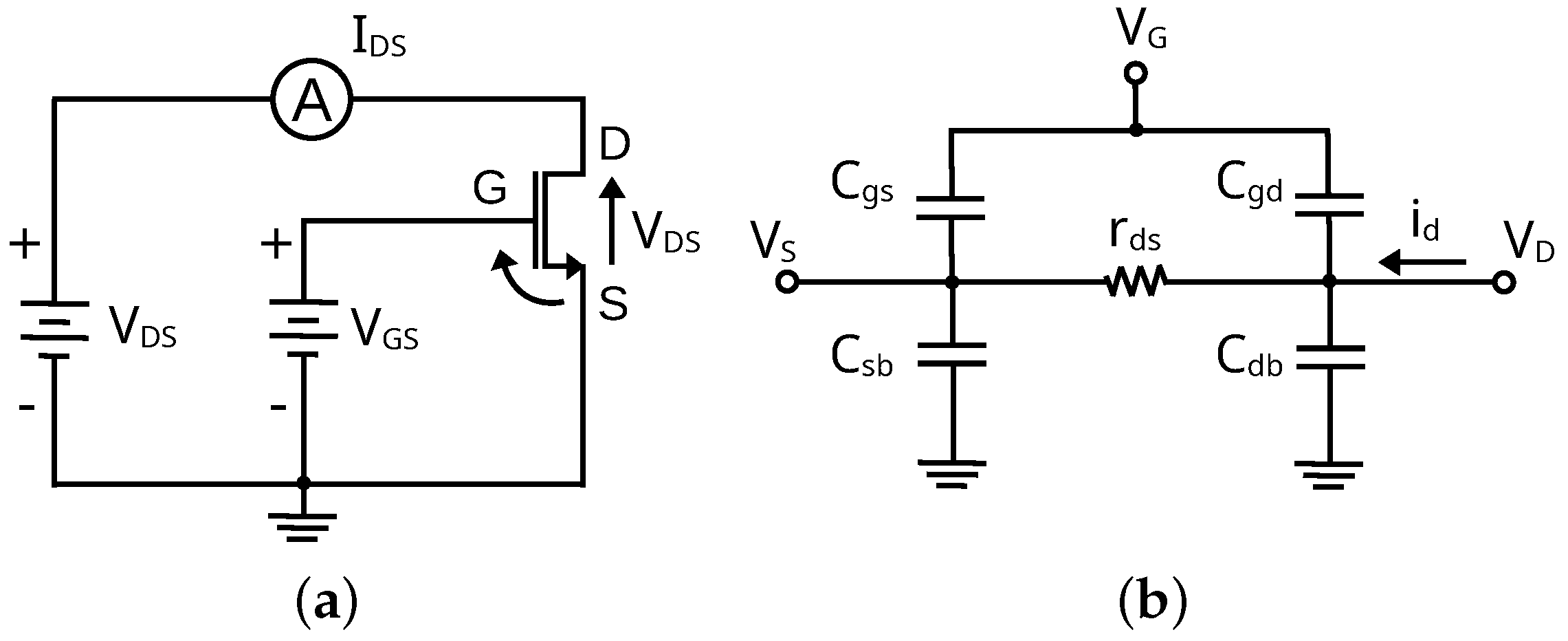
The / design procedure is a powerful sizing and biasing tool for MOSFET-based circuits [11,12]. The methodology exploits the ratio between the transconductance and the drain current as they are both width-dependent parameters to obtain a width-independent design variable. Since this ratio gives the ability of a MOSFET to generate a small-signal current gain from a DC bias current, the / ratio is often referred to as the MOSFET efficiency. The characterization of a MOSFET in terms of / ratio allows the derivation of the main performance metrics of a circuit to provide a width-independent sizing tool, allowing fast optimization and near-first-time successful design. A series of LUTs can be generated to avoid conventional SPICE iterative simulations, and designers can apply optimization algorithms to find optimal sizing and operating points or simply explore the design space more efficiently [31]. The first step consists of simulating several devices to fully characterize their behavior and build the LUTs with fundamental DC, AC, and noise parameters. These values can then be used to design LNAs given the specifications and circuit topology. The floating-body (FB) transistors of the GlobalFoundries 45RFSOI process design kit (PDK) are chosen to design the LNA. Since they are FB transistors, they do not possess substrate contact. To analyze their behavior, several geometries are simulated to fully characterize the behavior of the FETs in the selected kit. The total width (W) is varied from 20 to 120 μm in steps of 5 μm; the length (L) comes in discrete values of 32, 40, and 48 nm; and the unit finger width () is varied from 0.5 to 2 μm, which is the maximum range available in the PDK. In addition, the DC voltage is varied from 0 V to 1 V in steps of 25 mV and is varied from 0 V to 1 V in steps of 25 mV, using the schematic shown in Figure 1a, which is used to simulate all the parameters analyzed in this section.
The DC parameters observed include the drain current , the threshold voltage , the gate-drain current , and the gate-source current . On the other hand, the AC parameters obtained are regular transconductance , gate-bulk transconductance , drain-source transconductance , and all FET capacitances (shown in Figure 1b, gate-source , gate-drain , source-bulk , drain-bulk ). Finally, the noise of the FET is characterized using two main parameters: STH and SFL (thermal and flicker noise, respectively).
To automate the sweeps and generate the LUTs efficiently, the simulations are automated using a single MATLAB script that performs the following tasks:
- Generates DC sweeps for all corners. These corners are generated by considering all possible combinations of process, temperature, and noise variations and depend on the PDK used. In this case, the combinations include typical (T), slow (S), and fast (F) devices with −40 °C, 16 °C, 125 °C and high-, nominal-, and low-noise corners.
- Maps the FET’s operating point parameters into the desired output variables to build a multidimensional MATLAB matrix from the Cadence database results.
- Generates the Spectre simulation netlists with the desired geometries and sweeps.
- Sequentially runs all the previously generated simulations.
- Generates a .mat file with the multidimensional data for each corner as a result.
The original code provided by [11,12] is adapted to accommodate the 45RFSOI PDK and the mentioned sweeps. A simple lookUp() function is then used to recover the desired values and plot the desired parameters. More information about this process can be found in [11,12].
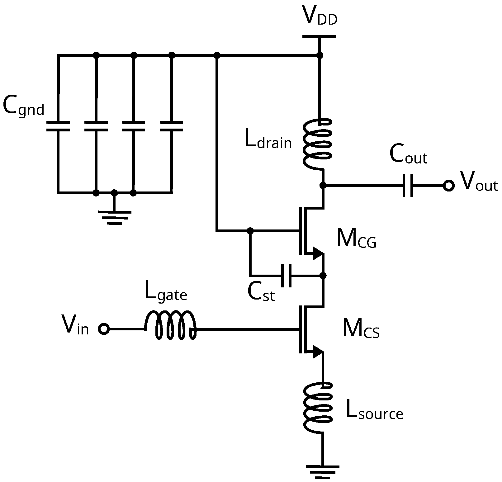
Since the Ka-band frequency range spans from 26.5 GHz to 40 GHz and the n257 frequency band (26.5 to 29.5 GHz) defined in the 3GPP 5G NR specification is particularly interesting for European mm-mave communications, a central frequency of 28 GHz is considered for the LNA design. To achieve high gain with a low NF and reasonable power consumption, a cascode topology, as shown in Figure 2, is selected [32,33,34,35,36]. It provides a high output impedance and higher input/output isolation compared to common-source and common-gate amplifiers, which allows the designer to cascade several stages if a higher gain is needed.
The inversion coefficient (IC) is used to identify the sub-threshold operation region of a MOSFET and is expressed using Equation (1), with being the MOSFT aspect ratio and , the specific current defined as (2) [37]. Details regarding the obtaining of for a given process can be found in [37]. The definition of results in the definition of three inversion regions: weak inversion (for ), moderate inversion (for ), and strong inversion ().
Following [14], a figure of merit for RF performance () can be defined, as shown in Expression (3), which can be employed to find the optimal inversion coefficient IC value for a given transistor in a high-frequency design.
The values of /, , and are presented in Figure 3a, Figure 3b and Figure 3c, respectively. Note that, as seen in Figure 3a, / is maximal in the weak inversion region and it decreases as IC moves toward the strong inversion region. On the other hand, the value (Figure 3b) is remarkably low in weak inversion and it rises as IC moves towards strong inversion. The result, as expressed in (3) and presented in Figure 3c, is that the moderate inversion region achieves the optimal trade-off and it benefits from the best combination of transistor efficiency / and high-frequency performance (). However, with this approach, the value of the input impedance () and optimal NF impedance () are not known yet. Impedance selection is critical in the design process, as the input matching network implementation severely affects the gain and noise performance of the LNA.
In conventional cascode amplifier design, where a common-source and a common-gate amplifier are used in series, simultaneous minimum NF and maximum gain matching can be achieved if source degeneration () is applied. Generally, the drain current density and transistor width are increased to move to the 50 circle, and then a single gate inductance () can be employed to match the circuit [38]. Therefore, a with a real part close to 50 is desired to facilitate impedance matching with a single gate inductor. To consider device geometries that allow this condition, assume the input impedance of a CS amplifier is given as (4) and the real part of the optimum source impedance is (5) [38,39]. From the state of the art, at Ka-band frequencies, an under 500 pH and an between 50 and 250 pH are conventionally used. Notice the parameters in (5) are known, and thus, the required width for = 50 can be obtained.
A total device width close to 50 μm is determined to satisfy the condition of an with a real part close to 50 . To provide some insights into the impedances defined in (4) and (5), a graphical representation is more clearly reflected in Figure 4. Proper choice of the source inductor value can ensure that and * are approximately equal for maximum power transfer. Then, a single gate inductor can be used to cancel the capacitive component at the gate of in Equation (4).
For the selected technology and the transistor employed, the total width value is determined to be 50 μm. The design approach consists of selecting a certain IC value that accommodates the specifications of the LNA. To decide which IC should be used, consider the following discussion. The transit frequency limits the frequency of operation and factors such as the achievable gain and NF [38]. The is closely related to the IC, as shown in Figure 3b. If the transistor’s is too close to 28 GHz, the LNA may not achieve a reasonable performance (low gain and high NF), but it may have low power consumption, as the lower the IC, the lower the drain current needed to bias the device. On the other hand, if the is very high (n times the operating frequency), the LNA will offer very high performance (high gain and low NF), but with high power consumption.
The advantage of using the / methodology is that the designer can access the LUTs and produce several sets of values to perform several designs. As an example to carry on with the design, consider three values: 44 GHz, 98 GHz, and 175 GHz. Since the value of is approximately given by (6) for a MOSFET and increases as does , the increases as the IC is augmented. The moderate inversion region is targeted for 44 GHz, the moderate-strong inversion region for 98 GHz, and the strong inversion region for 175 GHz. Operation in weak inversion results in a very high aspect ratio (W/L), and, therefore, the device presents significant capacitance with low drain current, resulting in poor high-frequency operation. The proof-of-concept design process is conducted for these values to make a comparison and select the best performance compromise. From Figure 3b, the value of IC is deduced, which is needed to obtain the DC operating point from the LUTs. In the case of the 44 GHz frequency, the corresponding value is 0.48. For 98 GHz, has a value of 1.58, and for 175 GHz, has a value of 4.92. The next step is to calculate the values of threshold voltage () and effective gate-source voltage or overdrive voltage ( or ) to properly bias the MOSFET. These parameters are plotted as a function of IC, as illustrated in Figure 5a,b.
The required voltage for the transistor to operate with the desired IC can be deduced from the previous figures and is given by Equation (7). sets the desired current flowing through the FETs, and thus, the higher the IC, the higher the needed to bias the device with the desired drain current. For the 44 GHz case, has a value of 182.41 mV to obtain a drain current of 0.67 mA; for the 98 GHz case, is 255 mV for = 2.2 mA; and for the 175 GHz case, 360 mV to set an of 6.8 mA.
To fully characterize the FETs, the transconductances for each IC are collected, which determine the transistor capability to produce a drain current change from an increment in . As shown in Figure 5c, an of 0.48 yields a of 12 mS; for = 1.58, is 28.72 mS; and for = 4.9, is 55.18 mS. As expected, the transconductance increases as does the drain current and is maximal in the strong inversion region. Similarly, the transistor efficiency (/) versus IC is sought, as shown in Figure 3a. As opposed to the transconductance, the transistor efficiency is usually maximal in weak inversion and it decreases as the operation region moves towards strong inversion; hence, for , is 18 S/A; for , is reduced to 13.07 S/A; and for , ) is only 8.07 S/A. With the values of / and available, the drain current can be solved from Equation (8).
At this point, the designer may wonder about the actual devices’ high-frequency performance for the selected IC values. Therefore, the and can be calculated, as shown in Figure 6. The case of suffers from a limited of 6.78 dB due to the lower and , as well as an increased of 1.37 dB for the same reason. Note these are ideal values assuming ideal matching networks are used and are expected to deviate to some extent once real components are added to the circuit. That means the actual circuit implementation with PDK components results in a higher NF and a lower gain due to finite Q factors and parasitic components. For the case of , the is significantly improved to 10.34 dB because of the increase in both and , and in this case is 1 dB. Finally, for the case of , the obtained is 13.08 dB and is as low as 0.86 dB. Since the original setup collects data from a single transistor, e.g., a common-source amplifier, both a higher gain and NF are expected when the cascode is set up.
The advantage of using this methodology is that LNAs can be designed by optimizing the power consumption for given specifications without the need for iterative simulations. Instead, a database with transistor parameters for a specific technology is available. In summary, Table 1 presents the values of the calculated parameters for the three IC values of 0.48, 1.58, and 4.92.
Table 1 illustrates the design trade-offs mentioned earlier. The most favorable among the three cases can be determined through the analysis of power consumption and a figure of merit (), as defined by Equation (9). Depending on the desired characteristics, the corresponding FoM definition and inversion region should be chosen. For instance, for our definition of , if low power consumption is desired, the weak inversion region should be selected. However, this choice comes with the flaw of increased and a lower compared to the other cases. On the other hand, if a high gain with a lower minimum noise figure is sought, it should be noted that the required increases, leading to higher power consumption. In contrast to low-frequency designs, in this case, the transistor area is not particularly relevant, as the impedance-matching components (inductors) occupy most of the space. Their area could be included in the definition of the FoM if the designer wants to account for them in a fairer comparison. These parameters enable us to assess and compare the quality of the different cases.
As shown in Table 1, in the case of , a high value of the is achieved with very low power consumption, but with unfavorable results, the NF is significantly high and the gain is under 10 dB. However, the = 5.7 indicates that the LNA is more efficient in generating a high gain and low NF performance from the current drawn. For , the LNA shows a maximum gain of 8.6 dB and an of 3.9 dB, but it draws only 0.67 mA. Whereas the power consumption of solution is remarkable, the gain and NF values are not in line with state-of-the-art K-band LNA designs. A gain above 10 dB and NF under 3 dB with ∼10 mA are considered state-of-the-art results. Notice the results for , with a increment of more than 5.5 dB compared to (to 14.2 dB) and reduction of 2 dB (to 1.9 dB), with a three-times-higher drain current (2.2 mA) required compared to . Considering similar works available in the literature, these values of and are closer to state-of-the-art K-band LNAs. As seen for , the values of and are improved further to 17 dB and 1.4 dB, respectively, but the current drawn increases as well. The required is three times that required to bias the LNA, yet the is only improved by 0.5 dB, and the maximum gain, by less than 3 dB. In the case of , slightly inferior results are obtained compared to , but with a much higher value and better power consumption. On the other hand, comparing to , the improvement in or power consumption is not as significant, meaning is not as efficient as , yet the results are inferior to state-of-the-art K-band LNAs. In the case of , the results can be further improved, but with a strong impact on the LNA’s power consumption with small gains in performance. Ultimately, the decision is to proceed with the layout design for = 1.76 μA, as it provides enough gain and NF to be in line with state-of-the-art solutions with the best trade-off between performance and power consumption, which will be explained in more detail in the following section.
After assembling the schematic, the DC operating point of the circuit is analyzed to verify the previously calculated values. There is an expected deviation in the DC parameters, since the FETs were simulated in a common-source configuration with a of 0.9 V. However, in the cascode the effective for each FET is reduced to ∼0.45 V, and due to the nature of short-channel devices, there is a drain current mismatch. Therefore, must be adjusted to ensure the drain current targeted value. Now, the LNAs’ matching components can be calculated. To bring the and to the center of the Smith chart, the values of , , and inductors (see Figure 2) are calculated. Additionally, a value of 50 fF has been established for all three cases to improve the .
3. MOSFET Characterization and Simulation Results
To include the effect of metal interconnections on FET performance early in the design process, the layout of the cascode is developed first [40]. The new component consists of the raw PDK FET device, an RCC (resistance, capacitance, and coupled capacitance) parasitic extraction of the low-level, thin metal layers, and an EM characterization of the high-level, thick metal layers to account for parasitic inductance. As indicated in expression (10), the value of can be optimized [38]. Note that is the gate resistance, is the source resistance, f is the working frequency, and is the unity current gain frequency.
The circuit is implemented using the GlobalFoundries 45 nm RFSOI PDK. The technology has seven copper (Cu) layers (M1-M3, C1, UA, OA, OB) and one aluminum (Al) layer with a thickness of 4.125 μm. The RCC extraction is obtained using Calibre xRC extraction, and the EM characterization is obtained from EMX Planar 3D software. A staircase configuration is used to optimize the NF () of this device by reducing parasitic capacitances and gate and source resistances. To facilitate DRC rules compliance and current flow, the FETs are divided into four instances. In addition, a capacitor ( in Figure 2) is added in metal layer C1 to improve device stability. The 3D view of the developed layout is presented in Figure 7.
Once the MOSFET characterization is availablem the schematic in Figure 2 is set up and the values of the inductors needed are adjusted to compensate for the deviations introduced by the new RCC + EM characterization of the cascode MOSFETs. The gate inductor is adjusted to 409 pH to achieve input impedance matching, is reduced to 313 pH, is reduced to 130 pH and substituted by a transmission line, and is adjusted to 24 fF to improve . In addition, for proper AC grounding, a number of 1 pF shunt capacitors are added at the gate of . The final cascode layout is shown in Figure 8.
A post-layout extraction of the S-parameters after EM simulation with all the passive components in the final circuit is performed to verify the LNA. The simulation results are presented in Figure 9, showing a gain of 11.4 dB and a NF of 3.8 dB at a central frequency of 28 GHz. Regarding the input and output return losses, an || of 12.7 dB and an || better than 10 dB are obtained. The LNA draws a total of 1.98 mW from a 0.9 V DC supply and occupies a core area of 0.723 × 0.598 mm2. As shown in Figure 9b, a two-tone simulation with 100 MHz spacing is conducted to verify the LNA’s linearity, demonstrating a P-1 dB of 1.8 dBm and an IIP3 of −1 dBm.
Table 2 presents a comparison with some of the most relevant state-of-the-art solutions. In [41], the authors develop a mm-wave multi-band LNA in 45 nm CMOS SOI using a three-stage differential cascode with interstage transformer-based matching networks to save area. It achieves a notable gain of 19.5 dB with an NF of 4.7 dB, but at the cost of high power consumption (59 mW). A single-ended-input, differential-output tunable K/Ka-band LNA operating at 28 and 39 GHz is demonstrated in a 65 nm CMOS in [42], maintaining a very low NF of 2.8 dB with a gain of 17.2 dB, yet with a very high power consumption of 28.5 mW. In [43], a 22 nm CMOS fully depleted-SOI low-power LNA with a single-stage cascode configuration is presented. It achieves a remarkable power consumption of only 4.6 mW, a gain of 7 dB, and an NF of 5 dB. A dual-band LNA in 22 nm CMOS FDSOI for 5G wireless systems is demonstrated in [44]; the authors report a high gain (19.3 dB) and a minimum NF of 5.2 dB with a power consumption of 11.4 mW in 0.27 mm2. The LNA achieves simultaneous dual-band operation by employing a two-stage single-ended cascode topology with carefully optimized transmission lines and capacitor-based matching networks. In [29], a wideband (14 and 31 GHz) LNA in 54 nm CMOS SOI is demonstrated, providing a low NF of only 1.4 dB with 12.8 dB gain. However, this LNA draws as much as 15 mW and occupies an area of 0.3 mm2. In contrast, we propose a low-power LNA that achieves a gain of 11.4 dB with only 1.98 mW power consumption, while maintaining an NF within the average range of the other state-of-the-art designs. The developed work demonstrates the methodology can effectively be used to obtain an LNA with a gain above 10 dB with a low NF. We report a very low power consumption with remarkably high performance at Ka-band frequencies.
4. Conclusions
The design of a low-power Ka-band cascode LNA using the / methodology is discussed in this work. The proposed circuit achieves a very low power consumption of only 1.98 mW. In addition, it is the first time the / approach is applied at Ka-band frequencies. The proposed circuit is developed with the 45 nm SOI PDK components. The LNA has a central frequency of 28 GHz as the circuit operates in the n257 frequency band defined by 3GPP NR for European mm-wave communications. The design approach presented involves the / methodology to exploit the advantages of sub-threshold operation in a high-frequency scenario, biasing devices in the moderate inversion region for a remarkable performance trade-off. A single MATLAB script is used to generate all the sweeps and the simulation netlists, to run the SPECTRE simulations, and to map the desired parameters in a multidimensional .MAT file containing all the LUTs needed to perform automated circuit design. We explore the procedure by providing a design example, from scratch to post-layout simulations, of a Ka-band cascode LNA obtaining a very-low-power, high-performance amplifier. The final circuit draws 1.98 mW from a DC supply of 0.9 V with a chip size of 0.43 mm2 excluding pads. After post-layout parasitic extraction and EM analyses, the circuit exhibits a gain of 11.4 dB, an NF of 3.8 dB, and an IRL better than 12 dB across the band of interest. Finally, a comparison is made with similar works available in the literature. The proposed circuit shows a very high performance, since the amplifier obtains a gain and NF in line with other works and a very low power consumption of only 1.98 mW.
Author Contributions
Methodology, J.d.P., S.L.K., D.G.-S. and J.T.-C.; Investigation, J.d.P., S.L.K., D.G.-S. and J.T.-C.; Supervision, J.d.P., S.L.K., D.G.-S. and J.T.-C.; Writing—original draft, D.G.-S. and J.T.-C.; Writing—review and editing, S.L.K. and J.d.P.; Visualization, J.d.P., S.L.K., D.G.-S. and J.T.-C.; Project administration, J.d.P., S.L.K., D.G.-S. and J.T.-C.; Funding acquisition, J.d.P. and S.L.K. All authors have read and agreed to the published version of the manuscript.
Funding
This work has been partially supported by grants PID2021-127712OB-C21 and PDC2023-145828-C22 funded by MCIN/AEI/10.13039/501100011033 (ERDF a way of making Europe, European Union Recovery and Resilience Mechanism), by the Canary Agency for Research, Innovation, and Information Society (ACIISI) by the TESIS2019010100 grant (European Social Fund) and by the Spanish Research Program "INVESTIGO" awarded to the "Fundación Canaria Parque Científico Tecnológico" funded by the Canarian Employment Service.
Institutional Review Board Statement
Not applicable.
Informed Consent Statement
Not applicable.
Data Availability Statement
Data is contained within the article.
Conflicts of Interest
The authors declare no conflicts of interest.
Abbreviations
The following abbreviations are used in this manuscript:
| Gate-Source Capacitance | |
| Gate-Drain Capacitance | |
| Source-Drain Capacitance | |
| Drain-Bulk Capacitance | |
| CMOS | Complementary Metal Oxide Semiconductor |
| IC | Inversion coefficient |
| Drain current | |
| Gate-Drain Current | |
| Gate-Source Current | |
| IRL | Input Return Loss |
| FB | Floating-Body |
| FoM | Figure of Merit |
| Drain-Source Transconductance | |
| Regular Transconductance | |
| Gate-Bulk Transconductance | |
| LNA | Low-Noise Amplifier |
| MMIC | Monolithic Microwave Integrated Circuit |
| MW | Microwave |
| NF | Noise figure |
| ORL | Output Return Loss |
| PDK | Process Design Kit |
| RF | Radiofrequency |
| RFIC | RF Integrated Circuit |
| UWB | Ultrawide Band |
| VDS | Drain-Source Voltage |
| VGA | Variable Gain Amplifier |
| VGS | Gate-Source Voltage |
| VTH | Threshold Voltage |
| SATCOM | Satellite Communications |
| SOI | Silicon-on-insulator |
| STH | Thermal Noise coefficient |
| SFL | Flicker Noise Coefficient |
| Unit Finger Width |
References
- Razavi, B. RF Microelectronics, 2nd ed.; Prentice Hall Communications Engineering and Emerging Technologies Series; Prentice Hall Press: Hoboken, NJ, USA, 2011; ISBN 0137134738. [Google Scholar]
- Lee, T.H. The Design of CMOS Radio-Frequency Integrated Circuits; Cambridge University Press: Cambridge, UK, 2004; ISBN 0521835399. [Google Scholar]
- Yeom, K.-W. Microwave Circuit Design: A Practical Approach Using ADS; Prentice Hall: Hoboken, NJ, USA, 2015; ISBN 0134085825. [Google Scholar]
- Piccinni, G.; Avitabile, G.; Coviello, G.; Talarico, C. Distributed amplifier design for UWB positioning systems using the gm over id methodology. In Proceedings of the 2016 13th International Conference on Synthesis, Modeling, Analysis and Simulation Methods and Applications to Circuit Design (SMACD), Lisbon, Portugal, 27–30 June 2016; pp. 1–4. [Google Scholar] [CrossRef]
- Elmeligy, K.; Omran, H. Fast Design Space Exploration and Multi-Objective Optimization of Wide-Band Noise-Canceling LNAs. Electronics 2022, 11, 816. [Google Scholar] [CrossRef]
- Piccinni, G.; Avitabile, G.; Coviello, G.; Talarico, C. Gm over ID design for UWB distributed amplifier. In Proceedings of the 2016 IEEE 59th International Midwest Symposium on Circuits and Systems (MWSCAS), Abu Dhabi, United Arab Emirates, 16–19 October 2016; pp. 1–4. [Google Scholar] [CrossRef]
- Belostotski, L.; Jagtap, S. Down with Noise: An Introduction to a Low-Noise Amplifier Survey. IEEE Solid-State Circuits Mag. 2020, 12, 23–29. [Google Scholar] [CrossRef]
- Khavari, A.F.; Mafinezhad, K. A New UWB LNA with 15 dB Gain in 90 nm CMOS with Current Reuse Topology. In Proceedings of the Electrical Engineering (ICEE), Iranian Conference, Mashhad, Iran, 8–10 May 2018; pp. 184–189. [Google Scholar] [CrossRef]
- Tripathy, D.; Nayak, D.; Biswal, S.M.; Swain, S.K.; Baral, B.; Das, S.K. A Low Power LNA using Current Reused Technique for UWB Application. In Proceedings of the 2019 Devices for Integrated Circuit (DevIC), Kalyani, India, 23–24 March 2019; pp. 310–313. [Google Scholar] [CrossRef]
- Chen, W.-W.; Yang, S.-D.; Cheng, K.-W. A 1.2 V 490 μW Sub-GHz UWB CMOS LNA with Current Reuse Negative Feedback. In Proceedings of the 2018 IEEE International Symposium on Circuits and Systems (ISCAS), Florence, Italy, 27–30 May 2018; pp. 1–4. [Google Scholar] [CrossRef]
- Jespers, P.G.A. The gm/ID Methodology, a Sizing Tool for Low-Voltage Analog CMOS Circuits; Springer Science and Business Media: Berlin/Heidelberg, Germany, 2009; ISBN 0387471014. [Google Scholar]
- Jespers, P.G.A. Boris Murmann, Systematic Design of Analog CMOS Circuits; Cambridge University Press: Cambridge, UK, 2017; ISBN 1107192250. [Google Scholar]
- Youssef, A.A.; Murmann, B.; Omran, H. Analog IC Design Using Precomputed Lookup Tables: Challenges and Solutions. IEEE Access 2020, 8, 134640–134652. [Google Scholar] [CrossRef]
- Enz, C.C.; Chicco, F.; Pezzotta, A. Nanoscale MOSFET Modeling: Part 2: Using the Inversion Coefficient as the Primary Design Parameter. IEEE Solid-State Circuits Mag. 2017, 9, 73–81. [Google Scholar] [CrossRef]
- Aueamnuay, C.; Kayyil, A.V.; Liu, J.; Thota, N.B.; Allstot, D.J. Gm/ID Design Considerations for Subthreshold-Based CMOS Two-Stage Operational Amplifiers. In Proceedings of the 2020 IEEE International Symposium on Circuits and Systems (ISCAS), Seville, Spain, 12–14 October 2020; pp. 1–5. [Google Scholar] [CrossRef]
- Hesham, B.; Hasaneen, E.-S.; Hamed, H.F.A. Design Procedure for Two-Stage CMOS Opamp using gm/ID design Methodology in 16 nm FinFET Technology. In Proceedings of the 2019 31st International Conference on Microelectronics (ICM), Cairo, Egypt, 15–18 December 2019; pp. 325–329. [Google Scholar] [CrossRef]
- Liu, J.; Lauga-Larroze, E.; Subias, S.; Fournier, J.-M.; Bourdel, S.; Galup, C.; Hameau, F. A Methodology for the Design of Capacitive Feedback LNAs based on the gm/ID Characteristic. In Proceedings of the 2018 16th IEEE International New Circuits and Systems Conference (NEWCAS), Montreal, QC, Canada, 24–27 June 2018; pp. 178–181. [Google Scholar] [CrossRef]
- Xie, Q.; Li, Z.; Shi, G. Design Space Exploration of Multi-Stage Op Amps by Symbolic Modeling and gm/ID Sampling. In Proceedings of the 2023 International Symposium of Electronics Design Automation (ISEDA), Nanjing, China, 8–11 May 2023; pp. 40–45. [Google Scholar] [CrossRef]
- Kumar, T.B.; Sharma, G.K.; Johar, A.K.; Gupta, D.; Kar, S.K.; Boolchandani, D. Design Automation of 5-T OTA using gm/ID methodology. In Proceedings of the 2019 IEEE Conference on Information and Communication Technology, Allahabad, India, 6–8 December 2019; pp. 1–5. [Google Scholar] [CrossRef]
- Castagnola, J.L.; García-Vázquez, H.; Dualibe, F.C. Design and optimisation of a cascode low noise amplifier (LNA) using MOST scattering parameters and gm/ID ratio. In Proceedings of the 2018 IEEE 9th Latin American Symposium on Circuits and Systems (LASCAS), Puerto Vallarta, Mexico, 25–28 February 2018; pp. 1–4. [Google Scholar] [CrossRef]
- Fiorelli, R.; Núñez, J.; Silveira, F. All-inversion region gm/ID methodology for RF circuits in FinFET technologies. In Proceedings of the 2018 16th IEEE International New Circuits and Systems Conference (NEWCAS), Montreal, QC, Canada, 24–27 June 2018; pp. 170–173. [Google Scholar] [CrossRef]
- Chung, J.; Iliadis, A.A. Modeling a High Linearity, Low Noise Gilbert Cell Mixer using Three Optimization Techniques. In Proceedings of the 2020 IEEE 63rd International Midwest Symposium on Circuits and Systems (MWSCAS), Springfield, MA, USA, 9–12 August 2020; pp. 790–793. [Google Scholar] [CrossRef]
- Piccinni, G.; Avitabile, G.; Coviello, G.; Talarico, C. Gilbert cell mixer design based on a novel systematic approach for nanoscale technologies. In Proceedings of the 2017 IEEE 18th Wireless and Microwave Technology Conference (WAMICON), Cocoa Beach, FL, USA, 24–25 April 2017; pp. 1–4. [Google Scholar] [CrossRef]
- Rudenko, T.; Nazarov, A.N.; Lysenko, V.S. The advancement of silicon-on-insulator (SOI) devices and their basic properties. Semicond. Phys. Quantum Electron. Optoelectron. 2020, 23, 227–252. [Google Scholar] [CrossRef]
- Wang, Y.; Cui, J.; Zhang, R. A K to Ka Band Single-ended to Balanced Ultra-wideband LNA in 45nm CMOS SOI. In Proceedings of the 2019 IEEE International Symposium on Radio-Frequency Integration Technology (RFIT), Nanjing, China, 28–30 August 2019; pp. 1–3. [Google Scholar] [CrossRef]
- Cuadrado-Calle, D.; George, D.; Fuller, G. A GaAs Ka-band (26–36 GHz) LNA for radio astronomy. In Proceedings of the 2014 IEEE International Microwave and RF Conference (IMaRC), Bangalore, India, 15–17 December 2014; pp. 301–303. [Google Scholar] [CrossRef]
- Cetin, T.; Onol, C.; Selcuk, G. A Ka-Band Front-End in 100nm GaAs Process for In-Band Full Duplex Communications. In Proceedings of the IEEE EUROCON 2019—18th International Conference on Smart Technologies, Novi Sad, Serbia, 1–4 July 2019; pp. 1–4. [Google Scholar] [CrossRef]
- Dilshad, U.; Chen, C.; Altaf, A.; Miao, J. An Ultra-Broadband K Ka-Band (17–40 GHz) LNA MMIC in 0.15 μm GaAs pHEMT. In Proceedings of the 2019 International Conference on Microwave and Millimeter Wave Technology (ICMMT), Guangzhou, China, 19–22 May 2019; pp. 1–3. [Google Scholar] [CrossRef]
- Li, C.; El-Aassar, O.; Kumar, A.; Boenke, M.; Rebeiz, G.M. LNA Design with CMOS SOI Process-l.4dB NF K/Ka band LNA. In Proceedings of the 2018 IEEE/MTT-S International Microwave Symposium—IMS, Philadelphia, PA, USA, 10–15 June 2018; pp. 1484–1486. [Google Scholar] [CrossRef]
- Dahlman, E.; Parkvall, S.; Sköld, J. 5G NR: The Next Generation Wireless Access Technology, 1st ed.; Academic Press Cambridge: Cambridge, MA, USA, 2018. [Google Scholar] [CrossRef]
- Castagnola, J.L.; Dualibe, F.C.; Laprovitta, A.M.; García-Vázquez, H. A Novel Design and Optimization Approach for Low Noise Amplifiers (LNA) Based on MOST Scattering Parameters and the gm/ID Ratio. Electronics 2020, 9, 785. [Google Scholar] [CrossRef]
- Kong, S.; Lee, H.-D.; Jang, S.; Park, J.; Kim, K.-S.; Lee, K.-C. A 28-GHz CMOS LNA with Stability-Enhanced Gm-Boosting Technique Using Transformers. In Proceedings of the 2019 IEEE Radio Frequency Integrated Circuits Symposium (RFIC), Boston, MA, USA, 2–4 June 2019; pp. 7–10. [Google Scholar] [CrossRef]
- Elkholy, M.; Shakib, S.; Dunworth, J.; Aparin, V.; Entesari, K. A Wideband Variable Gain LNA with High OIP3 for 5G Using 40-nm Bulk CMOS. IEEE Microw. Wirel. Compon. Lett. 2018, 28, 64–66. [Google Scholar] [CrossRef]
- Qin, P.; Xue, Q. Compact Wideband LNA with Gain and Input Matching Bandwidth Extensions by Transformer. IEEE Microw. Wirel. Compon. Lett. 2017, 27, 657–659. [Google Scholar] [CrossRef]
- Lee, S.; Park, J.; Hong, S. A Ka-Band Phase-Compensated Variable-Gain CMOS Low-Noise Amplifier. IEEE Microw. Wirel. Compon. Lett. 2019, 29, 131–133. [Google Scholar] [CrossRef]
- Nawaz, A.A.; Albrecht, J.D.; Ulusoy, A.Ç. A Ka/V Band-Switchable LNA with 2.8/3.4 dB Noise Figure. IEEE Microw. Wirel. Compon. Lett. 2019, 29, 662–664. [Google Scholar] [CrossRef]
- Enz, C.; Chicco, F.; Pezzotta, A. Nanoscale MOSFET Modeling: Part 1: The Simplified EKV Model for the Design of Low-Power Analog Circuits. IEEE Solid-State Circuits Mag. 2017, 9, 26–35. [Google Scholar] [CrossRef]
- El-Aassar, O.; Rebeiz, G.M. Design of Low-Power Sub-2.4 dB Mean NF 5G LNAs Using Forward Body Bias in 22 nm FDSOI. IEEE Trans. Microw. Theory Tech. 2020, 68, 4445–4454. [Google Scholar] [CrossRef]
- Sayginer, M.; Rebeiz, G.M. A W-Band LNA/Phase Shifter with 5-dB NF and 24-mW Power Consumption in 32-nm CMOS SOI. IEEE Trans. Microw. Theory Tech. 2018, 66, 1973–1982. [Google Scholar] [CrossRef]
- Gao, L.; Wagner, E.; Rebeiz, G.M. Design of E- and W-Band Low-Noise Amplifiers in 22-nm CMOS FD-SOI. IEEE Trans. Microw. Theory Tech. 2020, 68, 132–143. [Google Scholar] [CrossRef]
- Han, F.; Liu, X.; Wang, C.; Li, X.; Qi, Q.; Li, X.; Liu, Z. A multi-band LNA covering 17–38 GHz in 45 nm CMOS SOI. Electronics 2022, 11, 3255. [Google Scholar] [CrossRef]
- Chen, H.-H.; Tsai, Z.-M. Ka-/K-Band Frequency-Reconfigurable Single-Input Differential-Output Low-Noise Amplifier for 5G Applications. IEEE Microw. Wirel. Technol. Lett. 2023, 33, 1297–1300. [Google Scholar] [CrossRef]
- Hietanen, M.; Rusanen, J.; Aikio, J.P.; Tervo, N.; Rahkonen, T.; Pärssinen, A. Ka-Band TDD Front-End with Gate Shunt Switched Cascode LNA and Three-Stack PA on 22nm FDSOI CMOS Technology. In Proceedings of the 2020 50th European Microwave Conference (EuMC), Utrecht, The Netherlands, 12–14 January 2021; pp. 945–948. [Google Scholar] [CrossRef]
- Xu, X.; Schumann, S.; Ferschischi, A.; Finger, W.; Carta, C.; Ellinger, F. A 28 GHz and 38 GHz High-Gain Dual-Band LNA for 5G Wireless Systems in 22 nm FD-SOI CMOS. In Proceedings of the 2020 15th European Microwave Integrated Circuits Conference (EuMIC), Utrecht, The Netherlands, 10–15 January 2021; pp. 77–80. [Google Scholar]
Figure 1.
Schematic diagram of the setup used to obtain the I−V curves of the FB−FET from GlobalFoundries 45RFSOI PDK (a) and representation of the device capacitances (b).
Figure 1.
Schematic diagram of the setup used to obtain the I−V curves of the FB−FET from GlobalFoundries 45RFSOI PDK (a) and representation of the device capacitances (b).

Figure 2.
Schematic diagram of the cascode LNA developed.

Figure 3.
Representation of / (a), (b), and (c) as functions of the inversion coefficient IC.

Figure 4.
Schematic used to obtain the input and optimal NF impedances.

Figure 5.
Simulation results of the overdrive voltage (a), threshold voltage (b), and transconductance (c) as functions of IC.
Figure 5.
Simulation results of the overdrive voltage (a), threshold voltage (b), and transconductance (c) as functions of IC.
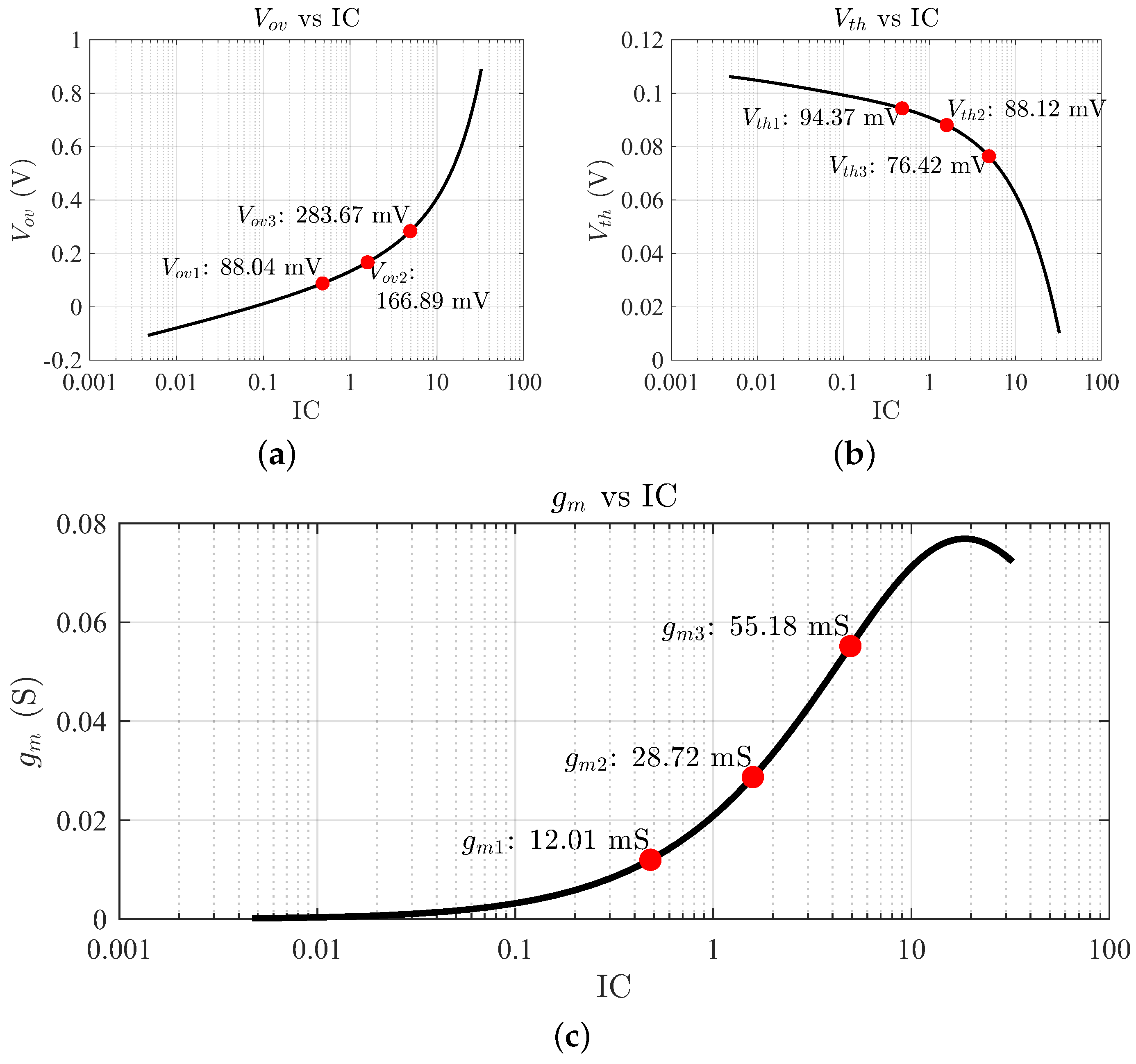
Figure 6.
Maximum gain and as a function of the inversion coefficient.

Figure 7.
3D view of the two MOSFETs used to design the cascode LNA.
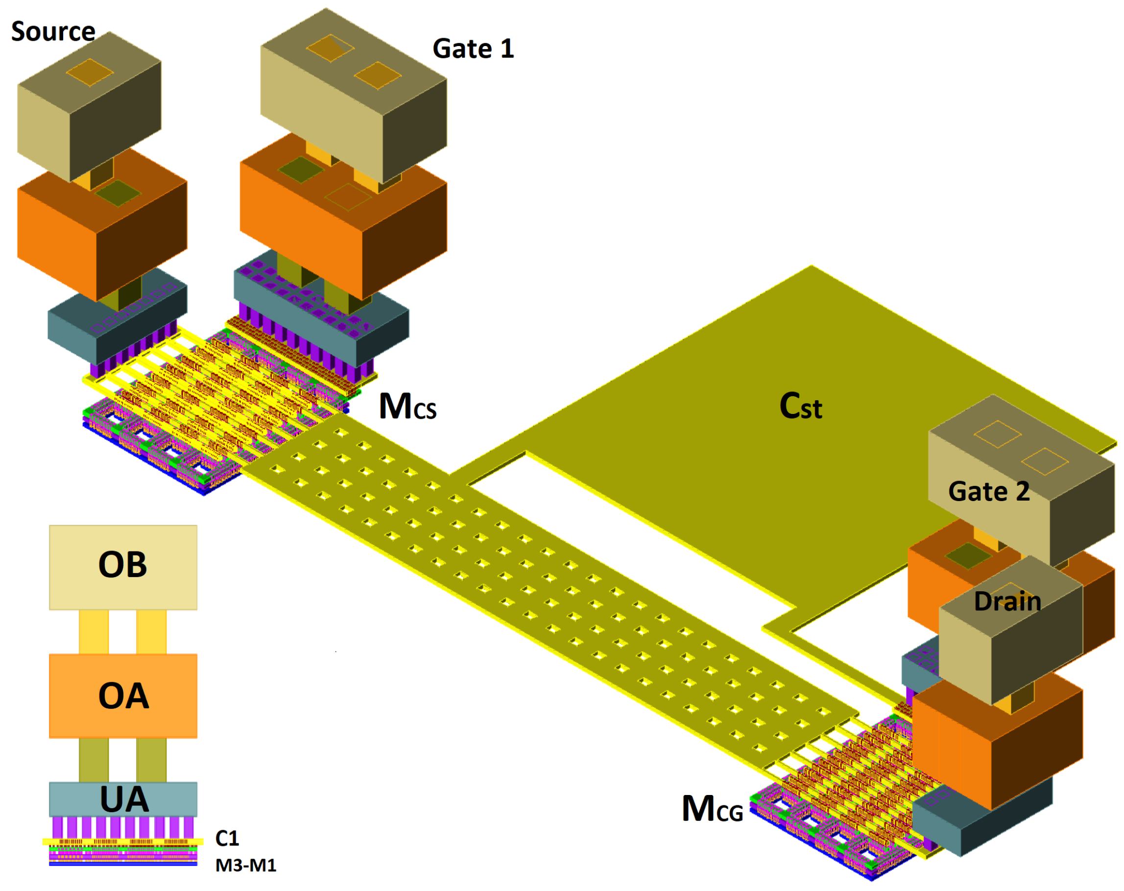
Figure 8.
Simplified frontal view of the cascode LNA final layout.

Figure 9.
Simulation results of the proposed LNA with the EM characterization of each passive component (a) and two-tone linearity simulation for the obtainment of the IIP3 (b).
Figure 9.
Simulation results of the proposed LNA with the EM characterization of each passive component (a) and two-tone linearity simulation for the obtainment of the IIP3 (b).


Table 1.
Values of the DC and AC parameters of the three selected ICs.
| Parameter | = 0.48 | = 1.58 | = 4.92 |
|---|---|---|---|
| (mV) | 182 | 255 | 360 |
| (mV) | 94 | 88 | 76 |
| (mA) | 0.67 | 2.2 | 6.8 |
| (mS) | 12 | 28.7 | 55.2 |
| / (S/A) | 18 | 13 | 8 |
| W/L | 1.25 k | 1.25 k | 1.25 k |
| (dB) | 3.9 | 1.9 | 1.4 |
| (dB) | 8.6 | 14.2 | 17 |
| (mW) | 0.6 | 1.98 | 6.2 |
| (pH) | 180 | 135 | 104 |
| (pH) | 458 | 408 | 352 |
| (pH) | 500 | 500 | 500 |
| 5.7 | 4.2 | 2 |
Table 2.
Overview of similar state-of-art LNAs with the proposed circuit.
| Reference | This Work | [41] | [42] | [43] | [44] | [29] |
|---|---|---|---|---|---|---|
| Tech. | 45 nm | 45 nm | 65 nm | 22 nm | 22 nm | 45 nm |
| SOI | SOI | CMOS | SOI | SOI | SOI | |
| BW (GHz) | 25.5–29.5 | 21–28 | 23.5–32.5 | 24–28 | 26.6–31.6 | 14–31 |
| Centre Freq. (GHz) | 27.5 | 24.5 | 27.5 | 26 | 29.1 | 22.5 |
| Supply (V) | 0.9 | 1 | 1 | 0.8 | 1.6 | 1.5 |
| Max Gain (dB) | 11.4 | 19.5 | 17.2 | 7 | 19.3 | 12.8 |
| Threshold Gain (dB) | 8.4 | 16.5 | 14.2 | 4 | 16.3 | 9.8 |
| NF (dB) | 3.5–3.8 | 4.7 | 2.8–3 | 5 | 5.2 | 1.4 |
| IRL (dB) | 12.7 | – | 25 | 6 | 10 | 10 |
| ORL (dB) | 10 | – | – | – | 10 | 10 |
| (mW) | 1.98 | 59 | 28.5 | 4.6 | 11.4 | 15 |
| Meas./Sim. | Sim | Meas. | Meas. | Meas. | Meas. | Meas. |
| 3.03 | 0.14 | 0.4 | 0.608 | 0.65 | 2.08 | |
| Core area (mm2) | 0.43 | 0.42 | 0.157 | 0.1 | 0.27 | 0.3 |
Disclaimer/Publisher’s Note: The statements, opinions and data contained in all publications are solely those of the individual author(s) and contributor(s) and not of MDPI and/or the editor(s). MDPI and/or the editor(s) disclaim responsibility for any injury to people or property resulting from any ideas, methods, instructions or products referred to in the content. |
© 2024 by the authors. Licensee MDPI, Basel, Switzerland. This article is an open access article distributed under the terms and conditions of the Creative Commons Attribution (CC BY) license (https://creativecommons.org/licenses/by/4.0/).
Share and Cite
MDPI and ACS Style
Galante-Sempere, D.; Torres-Clarke, J.; del Pino, J.; Khemchandani, S.L. A gm/ID-Based Low-Power LNA for Ka-Band Applications. Sensors 2024, 24, 2646. https://doi.org/10.3390/s24082646
AMA Style
Galante-Sempere D, Torres-Clarke J, del Pino J, Khemchandani SL. A gm/ID-Based Low-Power LNA for Ka-Band Applications. Sensors. 2024; 24(8):2646. https://doi.org/10.3390/s24082646
Chicago/Turabian StyleGalante-Sempere, David, Jeffrey Torres-Clarke, Javier del Pino, and Sunil Lalchand Khemchandani. 2024. "A gm/ID-Based Low-Power LNA for Ka-Band Applications" Sensors 24, no. 8: 2646. https://doi.org/10.3390/s24082646
Note that from the first issue of 2016, this journal uses article numbers instead of page numbers. See further details here.