Article

Various Structures Based on Nickel Oxide Thick Films as Gamma Radiation Sensors

Electronic and Computer Engineering Department, University of Limerick, Plassey Technological Park, Limerick, Ireland
*
Author to whom correspondence should be addressed.
Sensors 2003, 3(6), 176-186; https://doi.org/10.3390/s30600176
Submission received: 1 April 2003 / Accepted: 29 April 2003 / Published: 30 June 2003

Abstract

:
Thick films of Nickel oxide (NiO) in the form of pn-junctions and planar structures with interdigitated electrodes were investigated for γ-radiation dosimetry purposes. Samples were fabricated using the thick film screen-printing technique. All devices were exposed to a disc-type 137Cs source with an activity of 370 kBq. They showed an increase in the values of current with the increase in radiation dose up to a certain level. Performance parameters of the devices, such as sensitivity to γ-radiation exposure and working dose region, were found to be highly dependant on the composition of the materials used.

Introduction

Accurate dosimetry traceable to national standards underpins the protection of the general public and workers across a wide range of activities including general engineering, radiation processing, nuclear power generation, research and use of radiation in medicine and defence. To meet this demand, considerable research into new sensors is underway, including efforts to enhance the sensors performance through both the materials properties and manufacturing technologies. The development of sensors needs to take advantages of the new performances obtained by controlling the physical and chemical properties of the materials.
Metal oxides are widely used in many technological applications, such as coating, catalysis, electrochemistry, optical fibers, sensors, etc [1,2]. Metal oxide sensors have been utilised for several decades for their low-cost and simplicity. However, issues with sensitivity, selectivity and stability have limited their use, often in favour of more expensive approaches [3,4]. The recent availability of various metal oxide materials in high-surface-area nanopowder form, as well as implementation of newly developed nanofabrication techniques, offer tremendous opportunities for sensor manufacturers. New preparation technologies and optimised deposition process are essential to achieve better control of the materials characteristics and consequently to improve the sensor performance. Electrochromic materials, for example Nickel oxide, are used in applications such as energy efficient "smart windows", glare-free and variable reflectance mirrors, high-contrast non-emissive information displays, switchable displays, devices for thermal control, semiconductor-based sensors, etc. [5,6]. In this work a number of NiO based thick films of various structures were investigated in terms of their use as gamma radiation sensors. Screen printing technology allows a reliable manufacturing of the sensing elements, with cost-effective mass production and good reproducibility. The detection of radiation was based on the fact, that the properties of the materials undergo changes upon the influence of gamma radiation. Semiconductor nuclear detectors generally employ one of a number of device configurations (planar, sandwich, grid, etc.) [7].
High-energy radiations, such as γ-rays, change the physical properties of the materials they penetrate. Reactivity of oxide materials is closely connected to the presence of oxygen vacancies [8]. Oxygen vacancies are naturally present in every oxide in the form of Shottky or Frenkel defects, and their concentration can be increased or reduced in several ways [2]. Oxygen vacancies are known as colour centres or F centres (from Farbe, the German word for colour); if the vacancy is localized at the surface a subscript s is added, Fs. F centres exist in three states, depending on their electronic charge. Diamagnetic oxygen vacancies can be either neutral, F, or doubly charged, F2+. In the former case two electrons are associated to the vacancy. Of particular interest for the characterization of oxygen vacancies are the paramagnetic F+ centres, consisting of a single electron trapped in the cavity formed by removing an oxygen anion, O- [2]. It is believed that ionising radiation causes structural defects (called colour centres) leading to their density change on increase in exposure to γ-rays [9].
The requirements of radiation sensors include high sensitivity and linear performance over the intended energy range, real-time response, low noise, and acceptable reliability under the exposure conditions [10]. Due to the large number of different applications, there are many alternatives of the radiation sensors. Different materials, geometric arrangements and different physical-detection techniques are used to optimise the trade-offs that exist among the requirements [10].
A number of efforts were devoted to investigate the influence of radiation on the properties of metal oxide materials [11,12,13,14]. Gamma irradiation dose of 106–5×10⁷ rad degraded the electrical and dielectric properties of thin tantalum pentoxide layers obtained by RF sputtering and thermal oxidation in terms of dielectric constant, oxide charge and leakage current [12]. After the electron and γ-ray radiation of Titanium oxide films prepared by the DC reactive sputtering method, the number of Ti4+ ions decrease in the transition layer, Ti4+ turns to Ti3+ according to the reaction 2TiO2 → Ti2O3+O [14]. The influence of ionising radiation on Nickel oxide and its mixture with other oxides prepared by various techniques has been explored [11,13]. Screen-printed NiO thick films showed decrease in the optical band gap after gamma radiation treatment [11]. Irradiation with 1MGy gamma rays of NiO led to changes in its both surface oxidative abilities and catalytic activities [13]. Deep understanding of physical properties of these materials under the influence of radiation exposure is vital for the effective design of dosimeter devices.
In this work values of radiation damage in pn-junctions and interdigitated structures were estimated from changes in the current-voltage characteristics of the manufactured devices. The threshold radiation damage dose depends on the thickness and the structure of the device, properties of the material and on the fabrication technique used.

Experimental Procedure

Polymer pastes were made of 95 wt.% of functional materials (pure or Carbon-filled NiO) and 5 wt.% of C8H18O3 with Ethylenglycolmonobutylether as a solvent. Screen printing method (DEK RS 1202 automatic screen printer) was used for the fabrication of various thick film structures. Throughout the experimental work, two different types of devices, namely 1) pn-junctions and 2) interdigitated planar structures were fabricated.
1) NiO paste was screen-printed on single side polished N〈111〉 silicon wafers to form pn-junctions having the thickness of p-type layers of 60 μm.
2) For the fabrication of interdigitated structures microscopic glass slides were used as substrates. Electrical contacts in the form of interdigitated pattern were 15 µm in thickness with 10 interdigits on each side and occupied the total area of 8x9 mm2. Commercial DuPont 4929 silver paste was used to manufacture the electrical contacts for all the devices. On top of them, radiation-sensitive layers of NiO-based polymer pastes (pure NiO, 0.1 wt% and 0.2 wt% Carbon-filled NiO) having thickness of 60 µm were printed. Adding various amount of Carbon powder into the pastes controls the conductivity of the films.
A disc type 137Cs radiation source with activity of 370 kBq was used for exposing the samples to γ-radiation at room temperature. A set of irradiations were performed changing the exposure time and hence the dose. During the irradiation to γ-rays, external environmental conditions, such as temperature, humidity and light illumination, were maintained constant to ensure they do not contribute to the response characteristic of these devices.

Results and Discussion

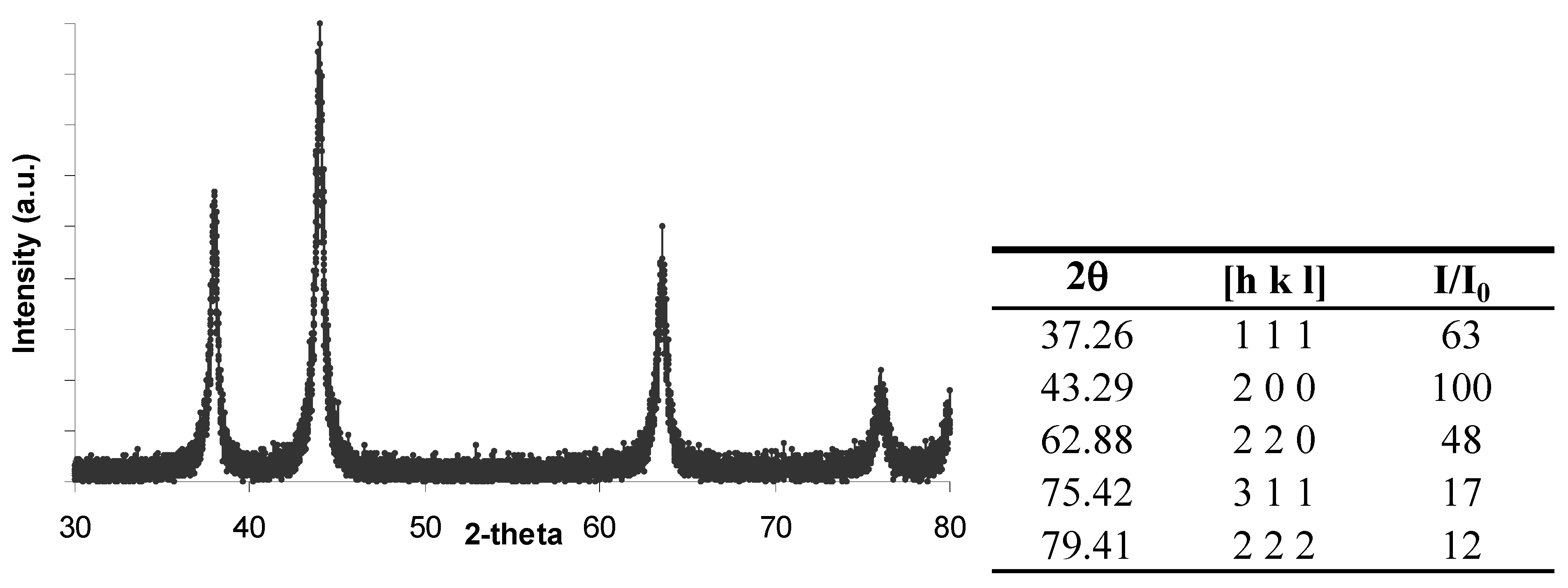
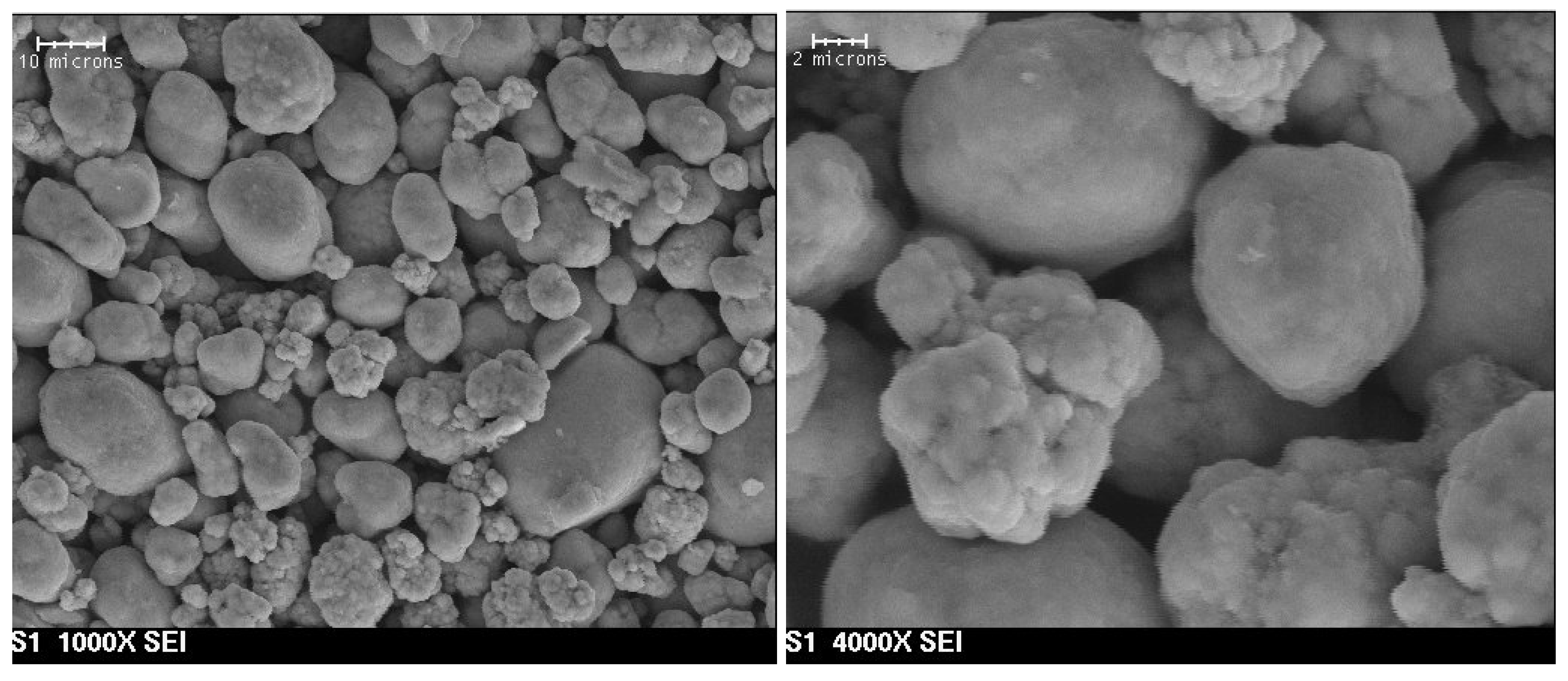
Structural Properties of NiO Thick Films

Figure 1 shows the XRD patterns of screen-printed NiO thick film along with the list of standard XRD peaks for NiO [15]. The XRD data highlighted that NiO thick films possess crystalline structure and exhibited the characteristic peaks of rock salt NiO. A small deviation of the peaks from the standard [15] is attributed to the material preparation technique used.
Since XRD technique provides an average structure for the crystalline phases with long-range structural order, the Scanning Electron Microscope (SEM) analysis of the samples was performed using Jeol JSM-840 SEM to reveal the morphology of the NiO films. Figure 2 illustrates SEM micrographs of NiO thick films with magnifications of 1000 and 4000 respectively. It demonstrates the porous surface morphology of these films that consist of the grains with variable sizes in the range of 1-10 μm.
Figure 1. XRD patterns of screen-printed NiO thick film and standard XRD peaks for NiO.
Sensors 03 00176 g001
Figure 2. SEM images of NiO thick film with magnifications of 1000 and 4000 respectively.
Sensors 03 00176 g002

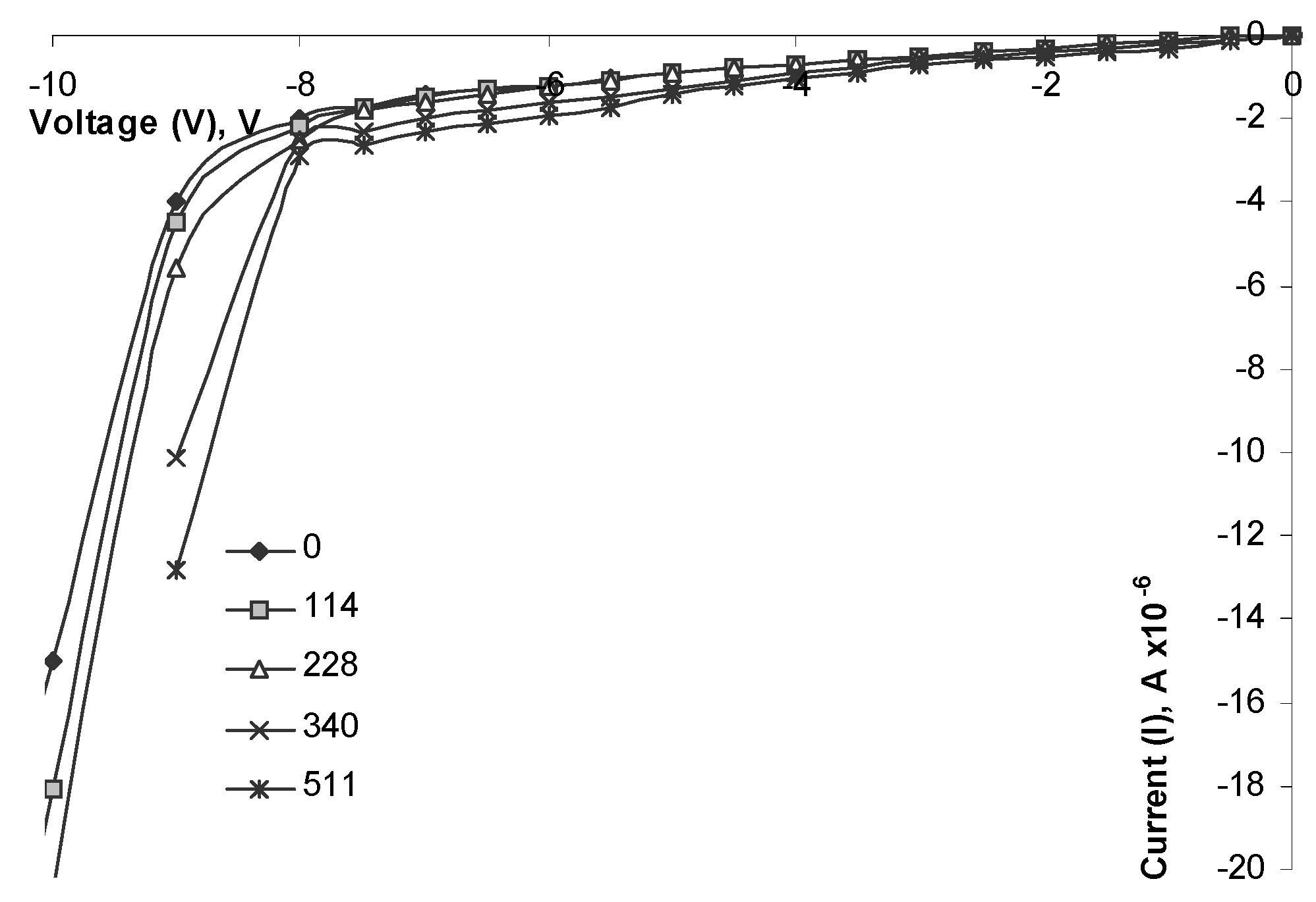
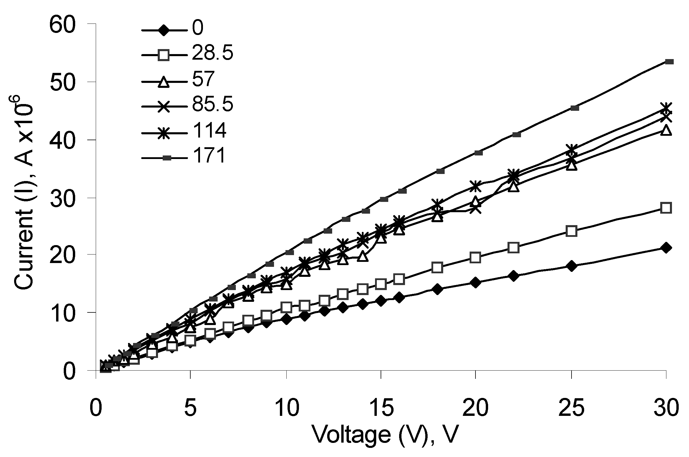
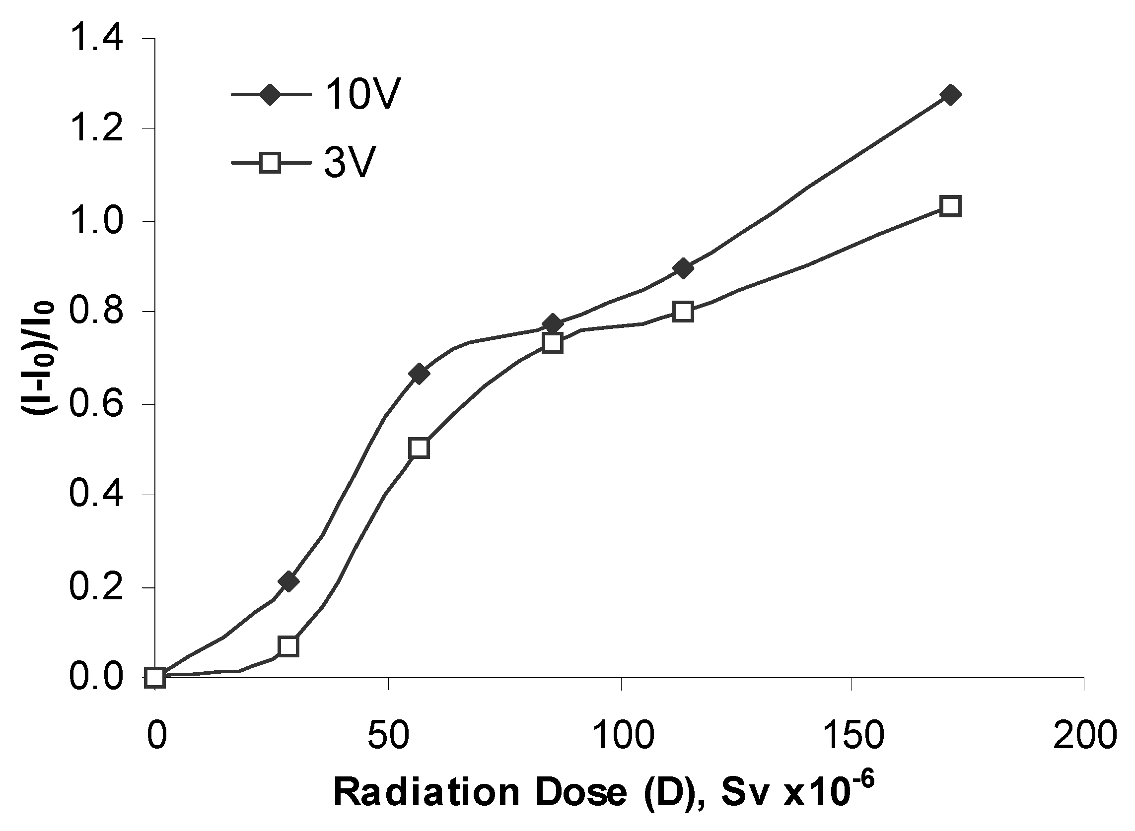
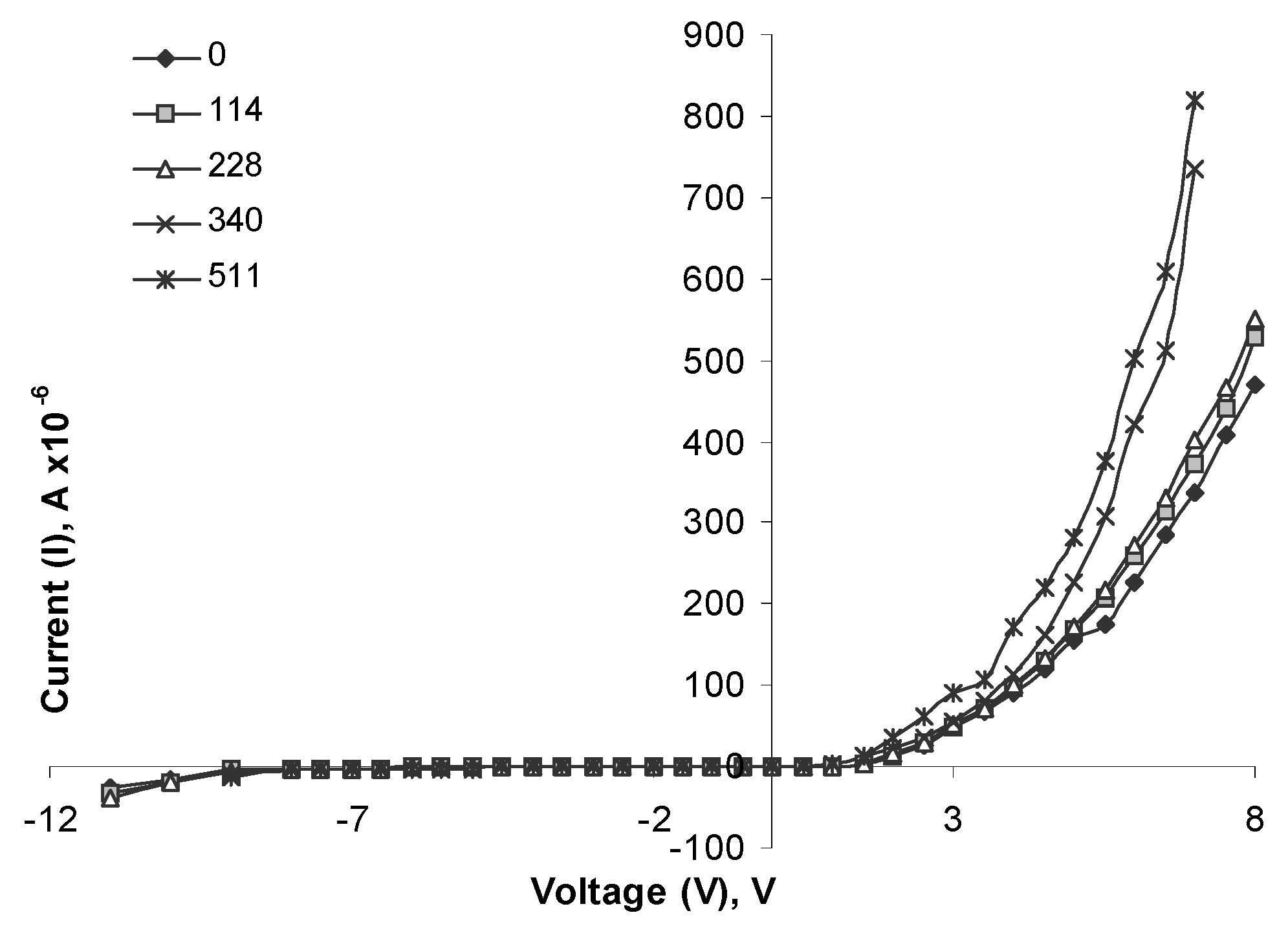
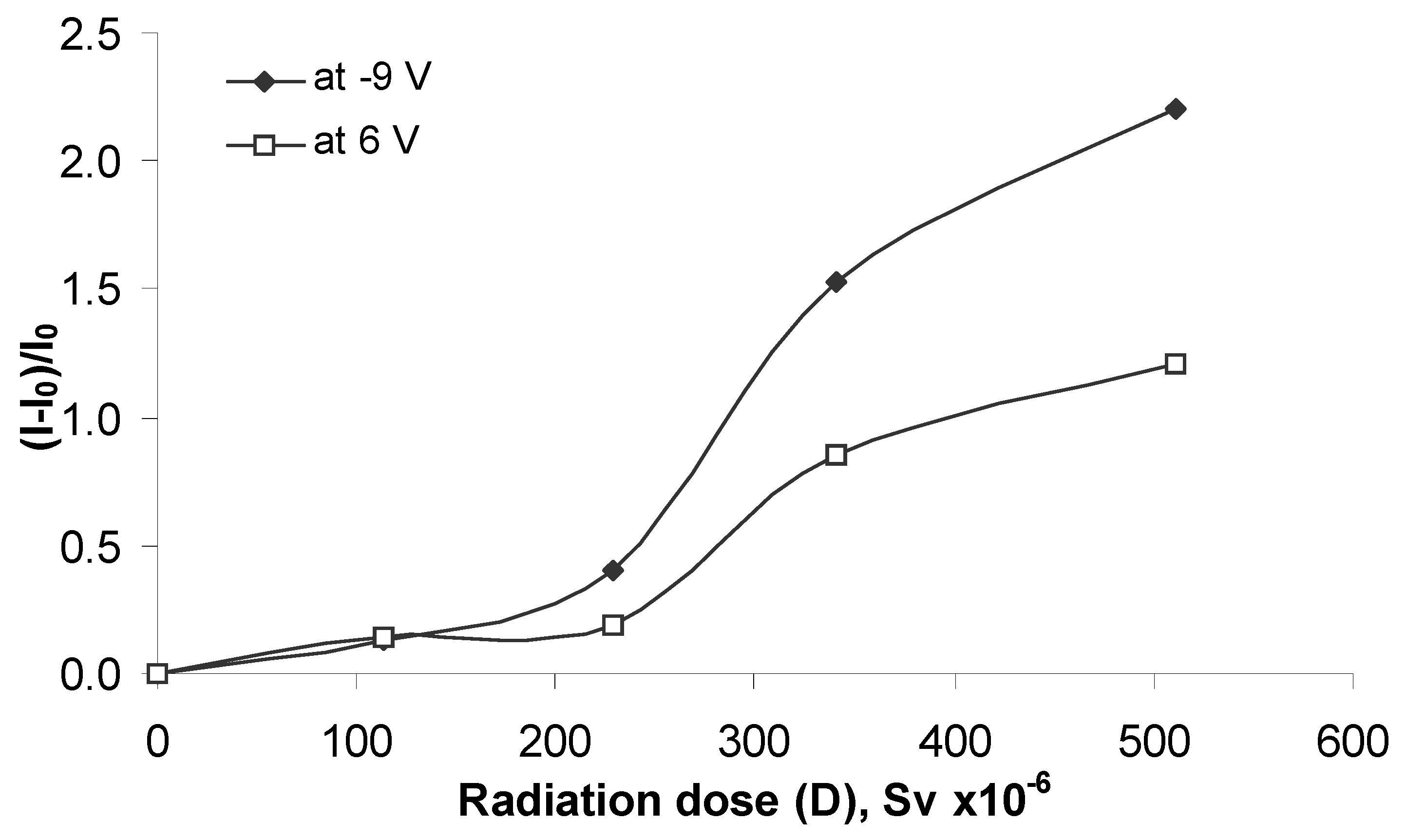
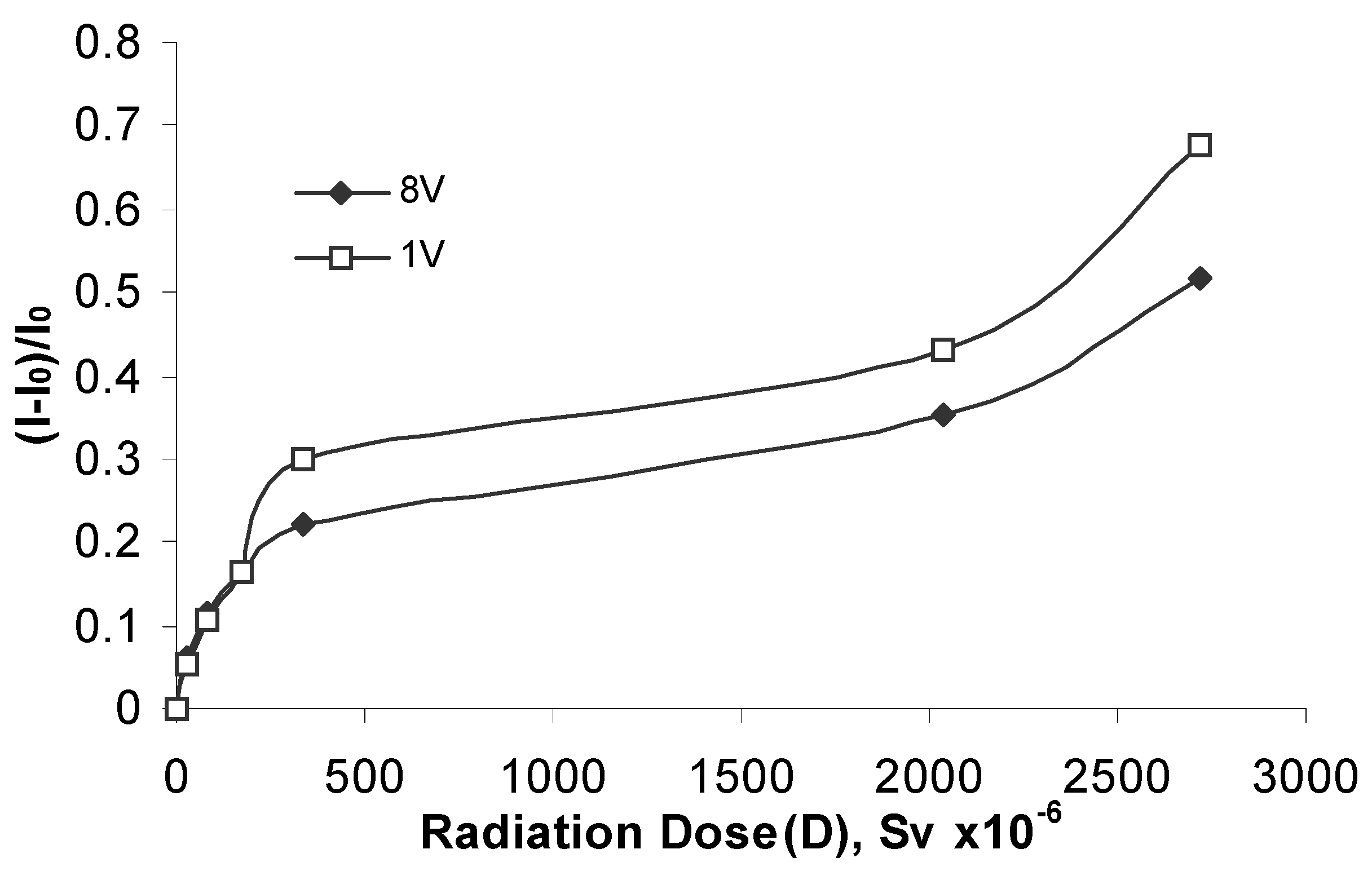
Effect of γ-radiation on NiO Diode Structures

Figure 3 shows typical current-voltage characteristics of NiO/Si samples, as-printed and γ-irradiated with different doses. Figure 4 demonstrates more clearly I-V plots for these devices under the reverse-biased conditions. In all graphs below, the exposed radiation doses are given in μSv units.
The values of both, the leakage current under the reverse-biased condition and the values of current when the diode is forward-biased, are increased considerably with the increase in radiation dose up to a level of 511 μSv. The parameter controlling leakage is the generation lifetime, which governs the rate of emission of holes in the depletion region [16]. To trace the radiation-induced changes in the values of current under the applied voltages of +6 V and -9V see Figure 5. It illustrates the dependences of normalized currents (I-I0)/I0 with dose for NiO/Si diodes. These curves may roughly be considered to consist of 3 regions. Linear increase in the values of currents was monitored with the increase in radiation to a dose of around 220 μSv. In the second region from 220 μSv to around 340 μSv a faster increase in the values of currents was observed. Further increase in radiation dose led to some kind of saturation in I-V plots.
Figure 3. Full-scale I-V plots of as-printed and γ-irradiated at different doses NiO/Si pn- junctions.
Sensors 03 00176 g003
Figure 4. I-V plots of as-printed and γ-irradiated NiO/Si diodes under the reverse-bias.
Sensors 03 00176 g004
The current increase was caused by the grain boundaries, which serve as current paths resulting in poor leakage current characteristics. Another reason for the worsening of the electrical properties is that the films were damaged by the creation of radiation defects in the form of broken Ni-O bonds. It is reasonable to assume that the increase in the leakage current after the influence of γ-radiation is partially attributed to the lowering of the barriers height at Ag/NiO interface. Similar effect of γ-rays was observed in Al/Ta2O5 interface because of building up a charge in Ta2O5 near this contact [12]. During irradiation process modification of Si-NiO interface takes place as a result of oxidation of Si wafer, leading to the enlargement of the mixed transition region, where SiO2 and the intermediate oxidation states of Si coexist. The latent defects, which are activated during irradiation, are in the form of oxide traps and are also responsible for deterioration of the device characteristics [12].
Figure 5. Dependence of normalized current (I-I0)/I0 with dose under the applied voltages of –9 V and +6 V for NiO/Si pn-junction structures.
Sensors 03 00176 g005

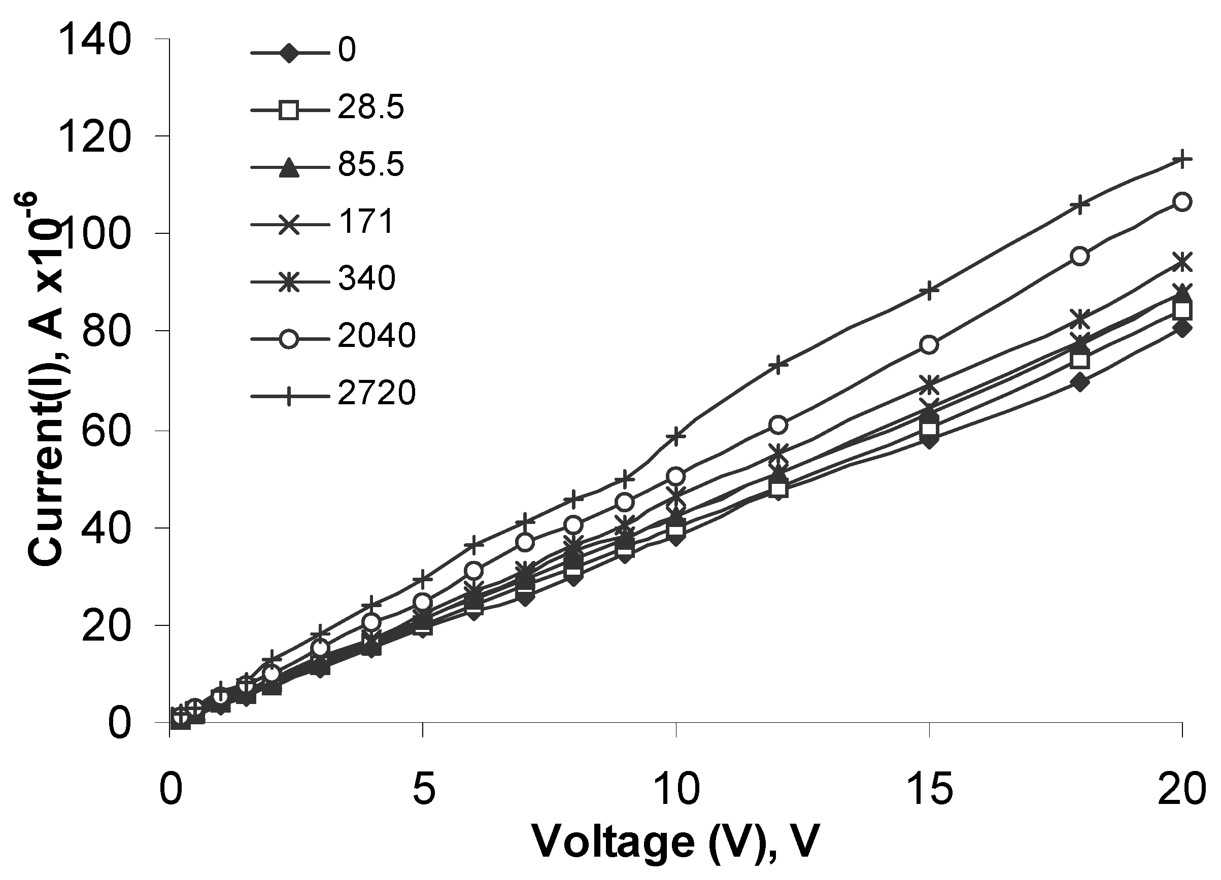
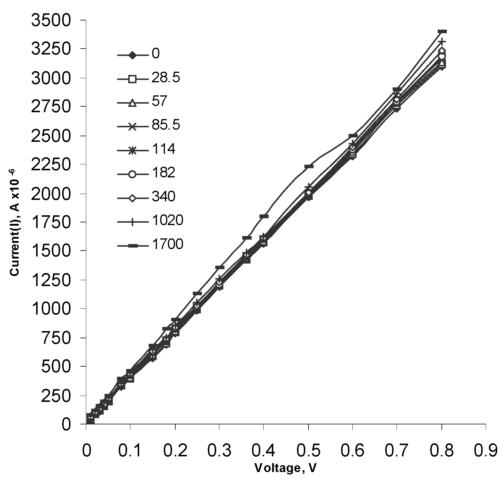
Effect of γ-radiation on Carbon-Filled NiO Planar Structures with Interdigitated Electrodes

In this work electrodes with interdigitated patterns were used to maximise the electrical admittance between two conducting structures in order to exploit the radiation-induced changes in the electrical properties of the materials printed over them.
Figure 6 shows plots of the I-V characteristics that were recorded for as-printed and γ-irradiated NiO planar structures with interdigitated electrodes. One can see that irradiation of the samples resulted in the significant alteration of current-voltage characteristics. Figure 7 depicts these changes, showing the increase in the values of normalized current (I-I0)/Io with the increase in radiation dose up to 171 μSv under the applied voltages of 3 V and 10 V.
Figure 6. I-V plots of as-printed and γ-irradiated at different doses NiO planar structures with interdigitated electrodes.
Sensors 03 00176 g006
Figure 7. Plot of normalized current (I-I0)/I0 with dose under the applied voltages of 10 V and 3 V for NiO interdigitated planar structures.
Sensors 03 00176 g007
To explore the effect of the composition on the performance of these devices, Carbon doping of 0.1 wt.% and 0.2 wt.% was used to increase the conductivity of polymer pastes. Increased conductivity of the films results in more pronounced signal response to external influences, such as γ-rays. As well it is beneficial from the circuitry point of view as it increase the signal/noise ratio and provides more reliable data output.
Figure 8. I-V plots of as-printed and γ-irradiated NiO planar structures doped with 0.1 wt.% of C.
Sensors 03 00176 g008
Figure 8 shows typical plots of the I-V characteristics of as-printed and γ-irradiated NiO planar structures doped with 0.1 wt.% of Carbon. Figure 9 shows the dependence of the normalized current (I-I0)/Io with the increase in radiation dose up to 2720 μSv under the applied voltages of 1 V and 8 V.
Figure 9. Plots of normalised current (I-I0)/I0 versus dose under the applied voltages of 1 V and 8 V for 0.1 wt.% Carbon-filled NiO planar structures.
Sensors 03 00176 g009
Carbon doping of NiO thick films of 0.1 wt.% resulted in larger increments in the values of current with the increase in radiation dose compared to the counterpart of pure NiO thick film structures. Moreover, this increase in values of current continued to be substantial at higher radiation doses thereby increasing its working range to 2720 μSv compared to 171 μSv of pure NiO samples.
Further increase in the level of Carbon doping makes the samples too conductive. Figure 10 shows plots of the I-V characteristics of as-printed and γ-irradiated NiO planar structures doped with 0.2 wt.% of Carbon. Figure 11 shows the dependence of the normalized current (I-I0)/Io with the increase in radiation dose up to 1700 μSv under the applied voltages of 0.1 V and 0.3 V for 0.2 wt.% Carbon-filled NiO planar structures with interdigitated electrodes. While the applied voltages were relatively low, the values of current were high, for example at the applied voltage of 0.8 V the value of current reached 3.5 mA. However such a device can find an application in low power supply conditions, for example in personal dosimetry. The substantial signal response has a trade-off in lowering the working radiation range of the devices.
Figure 10. I-V plots of as-printed and γ-irradiated at different doses NiO interdigitated planar structures doped with 0.2 wt.% of C.
Sensors 03 00176 g010
Figure 11. Plots of normalized current (I-I0)/I0 with dose under the applied voltages of 0.1 V and 0.3 V for 0.2 wt.% Carbon-filled NiO planar structures.
Sensors 03 00176 g011
The γ-radiation-induced changes in the electrical properties of all the samples were found to be similar to the dose response of most materials used in thermoluminescence (TL) dosimetry [17]. They usually show a linear, then supralinear, followed by saturating response and further increase in dose leads to their damage.
The details of the experimentally measured dose response depend on a great number of instrumental, radiation field and material parameters [17]. Similar feature of dose response was found in TL materials and lies in the dependence of the supralinearity on ionisation density, i.e., on gamma ray energy and on the type of radiation. The value of maximum supralinearity rapidly decreased with decreasing gamma ray energy: for 1.25 MeV gamma rays in LiF:Mg,Cu,P showed no supralinearity [17]. The difference in the properties of the materials used emerges as reasonable explanation to the changes of supralinear region in dependence of electrical parameters on radiation dose. However, the region of linear response is preferable in radiation dosimetry.
The model for colour centre kinetics assumes that the level of the radiation damage should be dose rate dependent because of the damage recovery [18]. As colour centres are created under irradiation, they also annihilate even under the room temperature. During irradiation, both annihilation and creation coexist; the colour centre density will reach equilibrium at a level depending on the dose rate applied. The creation and annihilation constants can be determined by using experimental data obtained under one particular dose rate, and can then be used to predict the behaviour of the same sample under different dose rates [18]. The threshold radiation damage dose depends on the thickness and the structure of the device, properties of the material and the fabrication technique used.

Conclusion

The possibility of using pure and Carbon-filled NiO thick films as sensitive materials to gamma radiation was explored. Various devices in the forms of pn-junctions and interdigitated planar structures were manufactured using screen-printing thick film technique. All devices were exposed to a disc-type 137Cs source with an activity of 370 kBq. They showed an increase in the values of current with the increase in radiation dose up to a certain level, which could be considered as a working region. For NiO/Si pn-junction, the values of both the leakage current under the reverse-biased conditions and the values of current when the diode was forward-biased increased considerably with the increase in radiation dose up to a level of 511 μSv.
The electrical properties of the films were highly dependant on the composition of the oxide materials used. It was experimentally demonstrated that it is possible to fabricate a device that would satisfy the requirement of particular application, in this case the sensitivity to γ-radiation exposure and working dose region. Planar NiO thick film structures with interdigitated electrodes showed increase in the values of current with the increase in radiation dose up to 171 μSv. Carbon doping of NiO thick films of 0.1 wt.% resulted in larger increments in the values of current and increasing the working range to 2720 μSv. NiO planar structures doped with 0.2 wt.% of Carbon showed the increase in the values of current with the increase in radiation dose up to 1700 μSv. The substantial signal response has a trade-off in lowering the working radiation range of the devices.
All these devices might be regarded as a cost-effective alternative for room temperature real time gamma radiation dosimetry.

Acknowledgments

This work was performed with the assistance of AMT Ireland at University of Limerick, as part of the RADSENAD project (ref. PRP00/AMT/06), sponsored by Enterprise Ireland Development Funds.

References

  1. Heinrich, V. E.; Cox, P. A. The surface science of metal oxides; Cambridge University Press: Cambridge, 1994. [Google Scholar]
  2. Pacchioni, G. Ab initio theory of point defects in oxide materials: structure, properties, chemical reactivity. Solid State Sciences 2000, 2, 161–179. [Google Scholar] [CrossRef]
  3. Faia, P. M.; Pereira, M. A.; Nunes, A. M.; Furtado, C. S. Electronic noses, a different approach to the sensitivity and selectivity issues. Journal of the European Ceramic Society 1999, 19, 883–886. [Google Scholar] [CrossRef]
  4. Hockensmith, C. M.; Goldsby, J. C.; Kacik, T. Thermal studies of new precursors to indium-tin oxides for use as sensor materials in the detection of NOx. Thermochimica Acta 1999, 340-341, 315–322. [Google Scholar] [CrossRef]
  5. Ragan, D. D.; Svedlindh, P.; Granqvist, C. G. Electrochromic Ni oxide films studied by magnetic measurements. Solar Energy Materials and Solar Cells 1998, 54, 247–254. [Google Scholar] [CrossRef]
  6. Neubecker, A.; Pompl, T.; Doll, T.; Hansch, W.; Eisele, I. Ozone-enhanced molecular beam deposition of nickel oxide (NiO) for sensor applications. Thin Solid Films 1997, 310, 19–23. [Google Scholar] [CrossRef]
  7. Schlesinger, T. E.; Toney, J. E.; Yoon, H.; Lee, E. Y.; Brunett, B. A.; Franks, L.; James, R. B. Cadmium zinc telluride and its use as a nuclear radiation detector material. Materials Science and Engineering: R: Reports 2001, 32, 103–189. [Google Scholar] [CrossRef]
  8. Pacchioni, G.; Pescarmona, P. Structure and stability of oxygen vacancies on sub-surface, terraces, and low-coordinated surface sites of MgO:: an ab initio study. Surface Science 1998, 412-413, 657–671. [Google Scholar] [CrossRef]
  9. Zhu, R. y. Radiation damage in scintillating crystals. Nuclear Instruments and Methods in Physics Research Section A: Accelerators, Spectrometers, Detectors and Associated Equipment 1998, 413, 297–311. [Google Scholar] [CrossRef]
  10. Audet, S.; Steigerwald, J. Semiconductor Sensors; Sze, S. M., Ed.; John Wiley & Sons, Inc.: New York, Chichester, Brisbane, Toronto, Singapore, 1994; Vol. pp. 271–329. [Google Scholar]
  11. Arshak, K.; Korostynska, O.; Harris, J. Gamma radiation dosimetry using screen printed nickel oxide thick films. In Proceeding of MIEL 2002, 23rd International conference on Microelectronics; pp. 357–360(2002).
  12. Atanassova, E.; Paskaleva, A.; Konakova, R.; Spassov, D.; Mitin, V. F. Influence of γ− radiation on thin Ta2O5-Si structures. Microelectronics Journal 2001, 32, 553–562. [Google Scholar] [CrossRef]
  13. Mucka, V.; Podlaha, J.; Silber, R. NiO-ThO2 mixed catalysts in hydrogen peroxide decomposition and influence of ionizing radiation. Radiation Physics and Chemistry 2000, 59, 467–475. [Google Scholar] [CrossRef]
  14. Zhang, J. D.; Fung, S.; Li-Bin, L.; Zhi-Jun, L. Ti ion valence variation induced by ionizing radiation at TiO2/Si interface. Surface and Coatings Technology 2002, 158-159, 238–241. [Google Scholar] [CrossRef]
  15. Powder Diffraction File, Joint Committee on Powder diffraction, International Center for Diffraction Data, Swarthmore, PA, 1987, Card. 4-0835.
  16. Holmes-Siedle, A. G.; Adams, L. Handbook of radiation effects; Oxford University Press: Oxford; New York, 1993. [Google Scholar]
  17. Horowitz, Y. S. Theory of thermoluminescence gamma dose response: The unified interaction model. Nuclear Instruments and Methods in Physics Research Section B: Beam Interactions with Materials and Atoms 2001, 184, 68–84. [Google Scholar]
  18. Deng, Q.; Yin, Z.; Zhu, R. Y. Radiation-induced color centers in La-doped PbWO4 crystals. Nuclear Instruments and Methods in Physics Research Section A: Accelerators, Spectrometers, Detectors and Associated Equipment 1999, 438, 415–420. [Google Scholar] [CrossRef]
  • Sample Availability: Available from the authors.

