Article

Sensing Arrays Constructed from Nanoparticle Thin Films and Interdigitated Microelectrodes

1
Department of Chemistry, State University of New York at Binghamton, Binghamton, New York 13902, USA
2
Watson Engineering School, State University of New York at Binghamton, Binghamton, New York 13902, USA
3
Department of Physics, State University of New York at Binghamton, Binghamton, New York 13902, USA
*
Authors to whom correspondence should be addressed.
Sensors 2006, 6(6), 667-679; https://doi.org/10.3390/s6060667
Submission received: 17 April 2006 / Accepted: 13 June 2006 / Published: 22 June 2006

Abstract

:
This paper describes the results of a study of a few design parameters influencing the performance of sensor arrays constructed from nanostructured thin films and interdigitated microelectrodes (IMEs). The nanostructured thin films on the IME devices were prepared from nonanedithiol (NDT) and mercaptoundecanoic acid (MUA) linked assemblies of 2-nm sized gold nanoparticles. The sensor array data in response to volatile organic compounds were collected and analyzed using fractional factorial experimental design and analysis of variance for understanding effects of the design parameters on the sensitivity. While the smaller value for the microelectrode space, width, and length generally led to higher response sensitivity, a strong dependence on the nature of the nanostructured thin films was found. The microelectrode space was the most important design parameter for NDT-based thin films. However, the microelectrode space, width, and length were found to play almost equally important roles for MUA-based thin films. The principal component analysis results for classification performances of the arrays consisting of a set of thin films have demonstrated the possibility of optimizing sensor arrays by appropriate selections of microelectrode parameters and nanostructured sensing films.

1. Introduction

The exploration of the interparticle properties of monolayer-capped nanoparticles and thin film assemblies has created interesting opportunities for chemical sensing in many significant ways. Examples include alkanethiolate-protected nanoparticles cast as metal-insulator-metal ensemble for chemiresistor sensing [1], ionic network bridged nanoparticles for vapor sensing via a swelling-induced alteration in length or chemical nature of electron tunneling [2], nanoparticles with different chain lengths or functional groups for piezoelectric sensing [3], and chemiresistor sensing [4]. Molecularly-mediated assembly of monolayer-capped gold nanoparticles via covalent bonding or hydrogen-bonding have recently been demonstrated for tuning sensitivity and specificity of both chemiresistive and piezoelectric sensors [5]. An important challenge is the development of the ability in correlating the array design parameters in terms of sensing nanostructure and sensor device properties [5, 6]. Molecularly-linked thin film assemblies of nanoparticles on interdigitated microelectrode platforms serve as an attractive system for addressing the challenge because of the viability in enhancing sensitivity, selectivity, detection limit and response time in terms of size, composition, functional group and spatial properties [5, 6, 7]. In addition, the coupling of nanostructures to the chemiresistive transducers has practical advantages, including easy array integration, rapid responses, and low power-driven portable format.
Several different nanostructured thin films and interdigitated microelectrodes (IME) of different design parameters in terms of microelectrode spatial properties have been used in constructing sensors [5, 6]. In the present work, the design of experiment (DOE) was used to study a set of IME devices with microelectrode spatial parameters, including 150 -300 pairs of gold (150 nm thick) electrodes with 5-10 μm finger width, 5-10 μm finger space, and 100 - 200 μm finger length. Currently, the limited knowledge on the correlation of such parameters with sensing properties constitutes an obstacle to the application of nanostructured sensing arrays in view of the complexity of chemical species in practical sensing environment. Sensor arrays combined with pattern-recognition analysis have demonstrated to be an effective approach to enhancing the selectivity and extending their applications [5, 6, 8]. In this work, we report findings of an investigation of the design of interdigitated microelectrodes coupled with nanostructured thin films in constructing sensor arrays for the detection of volatile organic compounds (VOCs). The correlation of the design parameters with the sensor properties provided information for the better design of sensor arrays.

2. Experimental

Chemicals. 11-mercaptoundecanoic acid (HS-(CH2)10-CO2H, MUA), 1,9-nonanedithiol (HS-(CH2)9-SH, NDT), and decanethiol (HS-(CH2)9-CH3, DT) were used as received (Aldrich). Vapors were generated from hexane (C6H14, Hx, 99.9%, Fisher), benzene (C6H6 (ϕ), Bz, 99.0%, Fisher), toluene (ϕ-CH3, Tl, 99.9%, J. T. Baker).
Gold nanoparticles of 2 nm core size encapsulated with decanethiolate (DT) monolayer shells were synthesized according to two-phase method [9] and a synthetic modification [10]. Details for the synthesis of our 2-nm gold nanoparticles (Aunm, 1.9 ± 0.7 nm) were previously described [11, 12].
Device Fabrication. IMEs of microelectrode parameters were fabricated by microfabrication, including 150 pairs of gold (150 nm thick) electrodes of 10 μm finger width, 10 μm finger space and 100 μm finger length, 200 pairs of gold electrodes of different finger width (5 μm, 10 μm), different finger space (10 μm, 5 μm) and 200 μm finger length, and 300 pairs of gold electrodes of 5 μm finger width, 5 μm finger space, and 100 μm finger length. The thin film electrodes were manufactured on glass substrate using Nordiko 2000 vacuum sputtering deposition system, in a base pressure below 1.5 × 10⁻⁶ torr with ultrahigh purity (99.999% pure) inert Ar acting as a sputtering gas. The IME device structure was patterned by photolithography at Cornell Nanoscale Facility (CNF). To address the problems associated with the lack of controllability over the electrode adhesion and spacing of IMEs by standard microfabrication techniques, we refined the each of our microfabrication steps, ranging from wafer cleaning, gold deposition, lithographic patterning, and wet chemical etching. Adhesion test, electrical testing, microscopic examination, and sensor array testing all showed that these IMEs produced by the refined processing control parameters meet the desired performance criteria. A 30nm Ti was sputtered onto glass substrates to act as an adhesion layer before the subsequent Au films of about 150 nm was deposited. The deposited Au/Ti films were subsequently processed at CNF clean-room facility. The first step of lithographic processing began with spin-coating with P-20 primer followed by a layer of S-1813 photoresist. These polymer-treated wafers were then baked on a hot plate for 120 sec, followed by proper exposure to the UV light from a Contact Aligner using a negative image chrome mask with designed patterns. Next, the exposed wafers were baked in oven for 85 mins. The wafers were then flood-exposed to the contact aligner for 60 seconds and then developed by MF-321 developer. The acid mixture used for etching away the Au film layer was HCl : HNO3 : H2O in 3:1:1 ratio with the acid bath at lukewarm temperature of 30°C. The etching period in the solution was typically 30∼32 sec for 150nm Au film. Once the upper layer of the Ti/Au film was removed, the underlying Ti adhesion layer was etched for approximately 50 seconds with NH3OH : H2O2 (30%) mixture of 1:2 ratio at room temperature.
Preparation of Thin Film Assembly. The nanoparticle thin films prepared for the present work included two types: (1) NDT-linked nanoparticles (NDT-Aunm) and (2) MUA-linked nanoparticles (MUA-Aunm). The thin films were prepared via “exchanging-crosslinking-precipitation” route [11]. The reaction involved an exchange of linker molecule (NDT, MUA) with the gold-bound alkanethiolates, followed by crosslinking and precipitation via either Au-S bonding at both ends of NDT, or hydrogen bonding at the carboxylic acid terminals of MUA. The IME substrates of the four different designs were then immersed into the same solution of the mixed nanoparticles and thiols at room temperature, and solvent evaporation was prevented during the film formation. The thickness of the thin films grown on the surface of the substrates was controlled by immersion time. Thin films of the same thickness were assembled on the IMEs of four different designs. The thin films thus produced were thoroughly rinsed with the solvent and dried under nitrogen. The NDT-Aunm coated sensors are denoted as NDT-Aunm/IME. Similar notations are for MUA-Aunm/IME.
Sensor Measurements. A computer-interfaced multi-channel multimeter (Keithley, Model 2700) was used to measure the lateral resistance of the nanostructured coating on IME. The resistance and frequency measurements were performed simultaneously with computer control. All experiments were performed at room temperature, 22 ± 1 °C. N2 gas (99.99%, Progas) was used as reference gas and as diluent to change vapor concentration by controlling mixing ratio. The gas flow was controlled by a calibrated Aalborg mass-flow controller (AFC-2600). The flow rates of the vapor stream were varied between 5 and 50 mL/min, with N2 added to a total of 100 mL/min. The vapor generating system followed the standard protocol [4b]. The vapor stream was produced by bubbling dry N2 gas through a bubbler of the vapor solvent using the controller to manipulate vapor concentration.
The resistance (R) was measured, and the relative differential resistance change ΔR/Ri was used for the evaluation of the vapor sorption responses. ΔR is the difference of the maximum and minimum values in the resistance response, and Ri is the initial resistance of the film [4a, 13]. The IME devices were housed in a test chamber with tubing connections to vapor and N2 sources. The setup of the vapor generating system followed the standard protocol [4b]. The vapor concentration in the unit of ppm moles per liter was calculated from the partial vapor pressure and the mixing ratio of vapor and N2 flows. Details of the IME experimental setup and measurement protocols were described in our recent report [5]. The IME electrode leads were connected to the multimeter. Nitrogen was used as carrier gas. Different concentrations of vapors were generated using an impinger system. At the beginning of the experiment, the test chamber was purged with pure nitrogen for 30 minute to ensure the absence of air and also to establish the baseline. The test chamber was purged with N2 for 10 minutes and test vapor for 10 minutes at the desired vapor concentration.
Our sensor array testing system involves switching of VOCs from one to another in order to establish the sensor profiles for each analyte. The propensity of this process to cross-contamination of analytes, especially low-vapor pressure VOCs, as a result of dead volumes in tubing and switching valves posed limitations on our sensor array testing system. To overcome or minimize this problem, we have built a multi-channel (currently 8 channels) and low dead-volume flow control and mixing system (Modular Platform Components (MPC) technology from Swagelok). The MPC defines the interface for surface mount fluid distribution components with elastomeric sealing devices used within the process analyzer and sample-handling system with minimum dead-volume and virtually no cross-contamination. Importantly, it allows control of mixing of different VOCs in most effective ways.

3. Results and Discussion

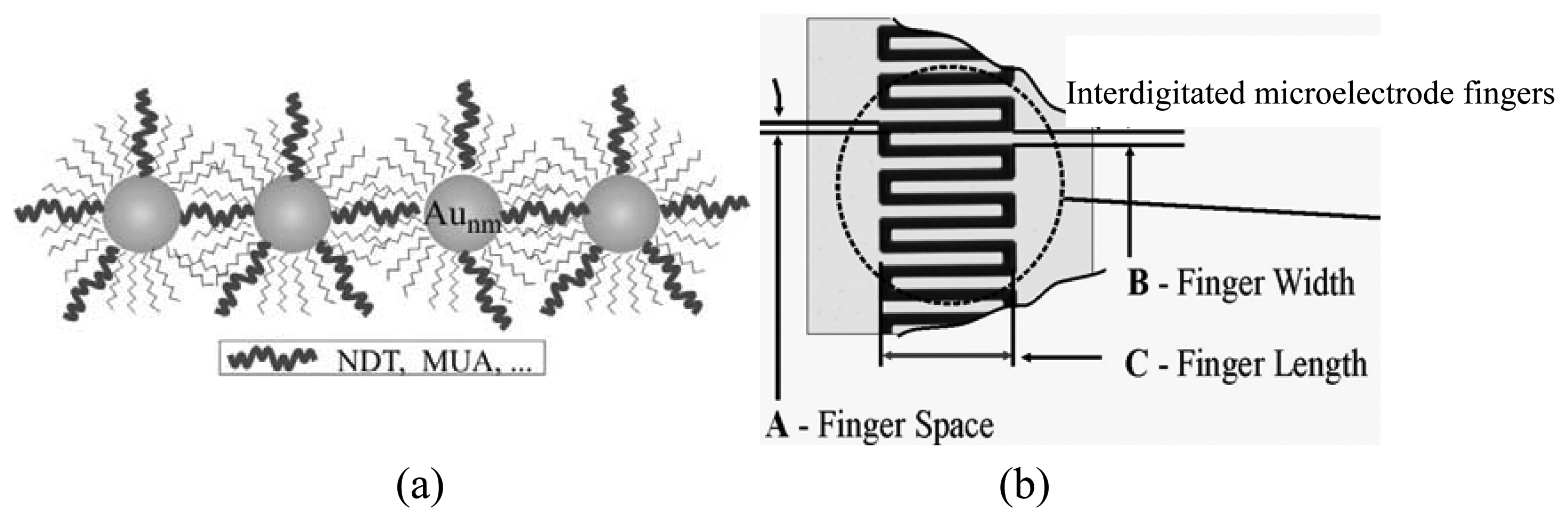
3.1. Sensor Device Characterization

The design parameters of the thin film coated IME arrays were first evaluated using DOE techniques. DOE is a widely used tool for effectively and efficiently designing and conducting experiments with certain principles [14]. Statistical methods, such as Analysis of Variance (ANOVA) [14,15], are then used to analyze the experimental data to draw meaningful conclusions. To examine the effects of three factors/parameters, finger space (FS), finger width (FW), and finger length (FL), in the sensor design, one-half of the 23, 23-1, fractional factorial experiment with single replicate is designed, in which 3 represents the 3 interested factors and 2 implies each one with two levels. The nanostructured thin film assembly and the microelectrode design parameters of the IMEs are illustrated in Figure 1.
The structures of the nanostructured thin film assemblies and their preparation have been described in previous reports [5]. IME devices with Au electrodes of different finger width (FW, 5 μm, 10 μm), finger space (FS, 5 μm, 10 μm), and finger length (FL, 100 μm, 200 μm) and the four combinations of the different parameters are shown in Table 1. The analysis of effects of the factors on experimental responses can be performed to identify the significant factors. The statistical analysis on the results of the designed experiment is summarized in Section 3.3.
Table 2 summarizes the average initial resistance values for an array of NDT-Aunm and MUA-Aunm films on IMEs of four combinations of the different parameters under N2 purge. The differences in the initial conductivities reflect the differences of a combination of several parameters including interparticle distances, dielectric medium constants, and the design parameters for the IME sensing array.
Based on the comparison of the resistance values between MUA-Aunm and NDT-Aunm films on the same IME designs, initial resistance of MUA-Aunm is found to be about 150 times larger than that of NDT-Aunm. This finding is consistent with the interparticle spatial properties expected for the MUA and NDT linker molecules [5, 6]. The array sensing materials (NDT-Aunm, and MUA-Aunm,) differ from each other in terms of the chemical and physical nature of the mediator molecules, which include hydrophobicity and hydrogen-bonding property. The sensor arrays also differ from each other by the electrode parameters in the device design. Because of these differences, the thin film resistances differ from each other. The data indicated that the finger space had significant effects on the thin film resistance properties. The IMEs with smaller FS (#3 and #4) exhibited smaller initial resistance value than those with larger FS. This finding is qualitatively consistent with the expectation based on thin film conductivity. In addition, finger length also seemed to play an important role in the thin film resistance properties. By comparing the IMEs with the same finger space but different finger length, it is found that those with longer FL (e.g., #2 > #1, and #3 > #4) had smaller initial resistance values. There was a relatively insignificant effect of the finger width on the thin film resistance properties, in comparison with the influence of finger space.

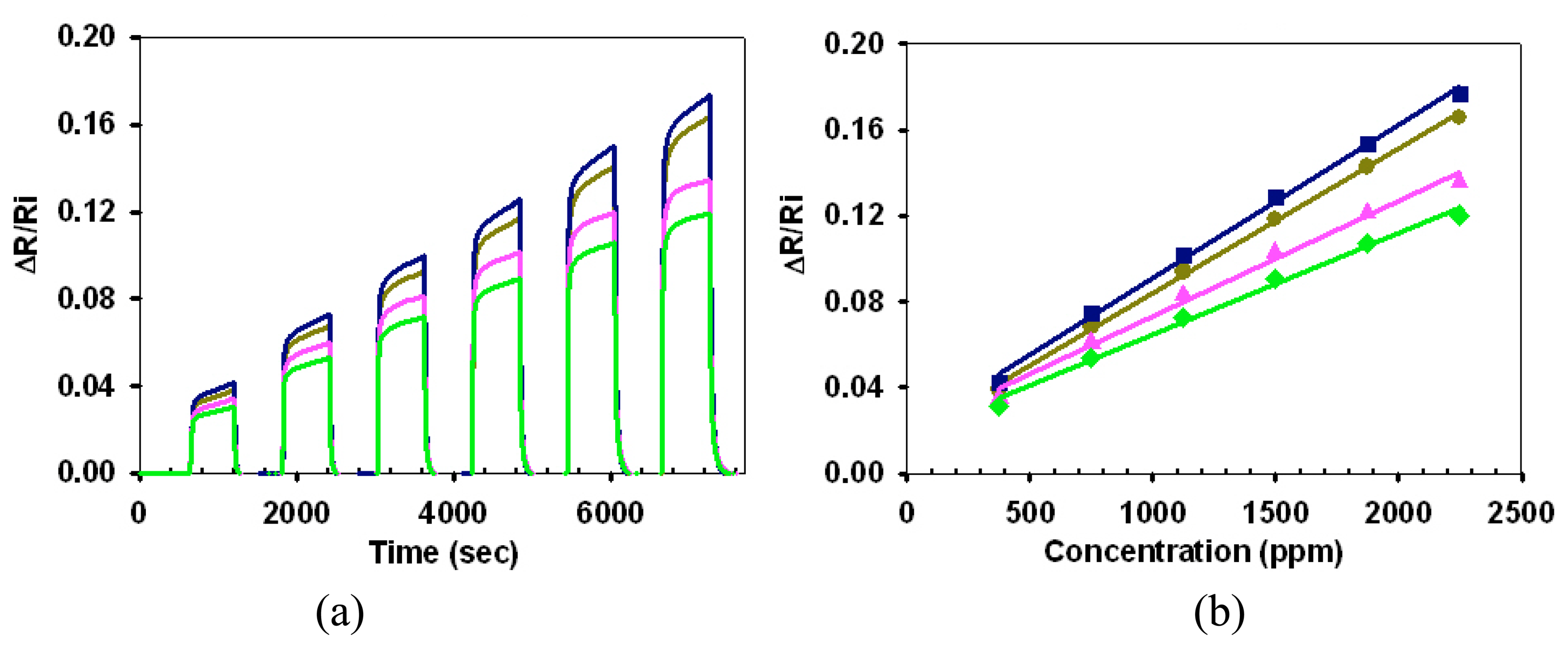
3.2. Array Response Characteristics

The response profiles for a sensing array of eight IME devices coated with NDT-Aunm and MUA-Aunm films were examined for their exposures to several volatile organic vapor analytes (e.g., hexane, benzene, toluene). Figure 2a shows a representative set of sensor response profiles to Hx vapor for a sensor array consisting of NDT-Aunm/IME. The sensor response sensitivity data are shown in Figure 2b. Similar response profiles for Bz and Tl vapors with subtle differences in response sensitivity were observed for NDT-Aunm films on IMEs of different microelectrode parameters. In view of the differences in the initial resistance for the different sensing films, we used the relative resistance change, ΔR/Ri, as a measure of the sensor response signal.
In general, the response characteristic in the above two sets of data shows a general profile of an increase in ΔR/Ri upon exposure to vapor followed by return to baseline upon purging with nitrogen. The response is relatively rapid and reversible. In most cases, the responses increased linearly with the vapor concentration. The slope serves as a measure of the response sensitivity. It is clear that these sensing array elements display linear responses to the concentrations of vapors. While the response profiles of the same vapors at different films are similar, the response sensitivities vary, as evidenced by the differences in the slopes of the linear relationships.
The above response data provide the basis for the comparison of the response sensitivities between NDT-Aunm film and MUA-Aunm film. Table 3 shows several sets of response sensitivities for three different vapors, hexane, toluene and benzene. In the comparison, response sensitivities are expressed in differential resistance change per ppm of vapor concentration, and they are also compared with data obtained with IMEs of different microelectrode design parameters, including those reported in our earlier reports [5, 6].
From Table 3, there are several important findings. First, the sensor devices with MUA-Aunm films exhibited higher sensitivities than those for NDT-Aunm films, reflecting the differences in interparticle distances, dielectric medium constants and chemical properties. Secondly, by comparing the data with those reported in our earlier work using IMEs with different design parameters, IMEs #3 and #4 design showed response sensitivities comparable to those reported earlier except the case of MUA-Aunm films in response to toluene and benzene. The reasons that caused this difference are not completely clear, but differences in film thickness might have played a role. Thirdly, in the case of thin films with smaller resistance values such as NDT-Aunm films, IMEs with smaller finger space exhibited higher sensitivities. This finding is consistent with the fact that smaller finger space leads to smaller initial resistance. The further analysis on the data in Table 3 is summarized in the following section.

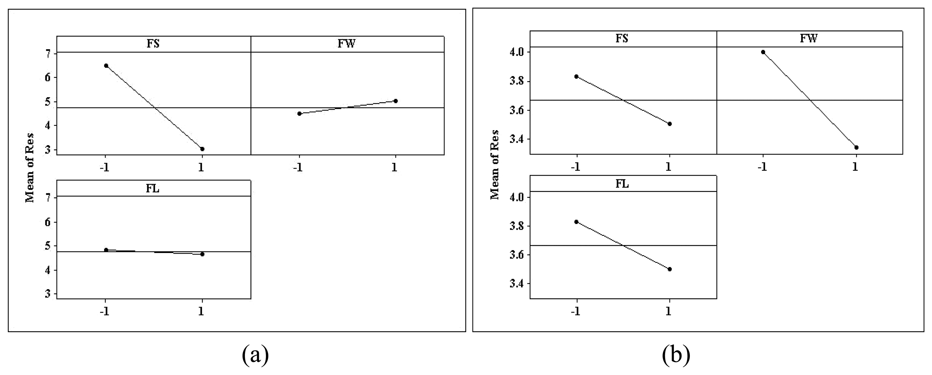
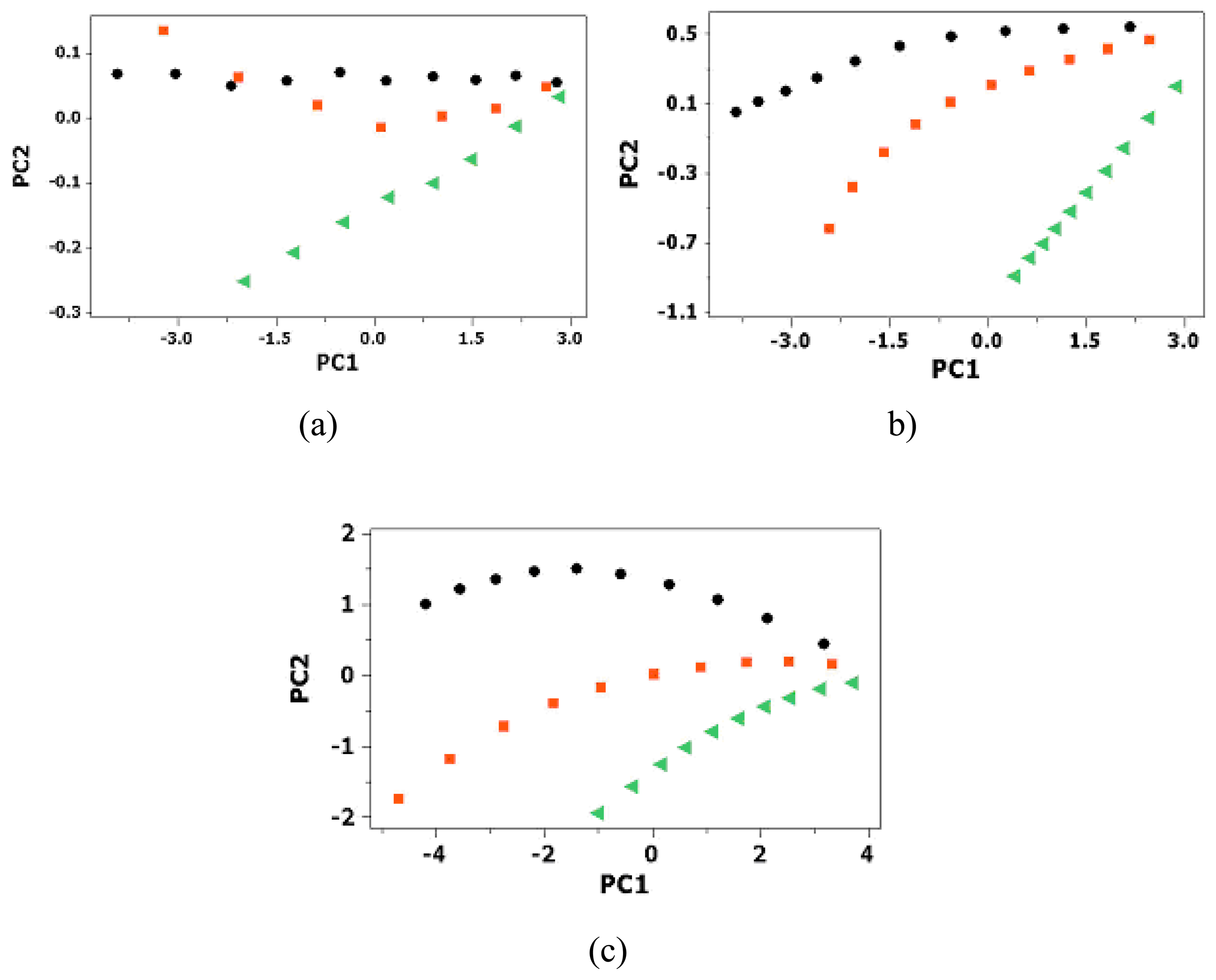
3.3. Statistical Analysis of Sensor Array Data

Sensitivity analysis. As discussed in Section 3.1, 23-1 fractional factorial design was used to investigate the effects of the three factors: finger space (FS), finger width (FW), and figure length (FL) on device performance. In this design, the responses sensitivities of the NDT-Aunm and MUA-Aunm films on IME devices of four different device design parameters to the three different vapors (hexane, benzene, and toluene) were used as the performance measures for the evaluation. The average sensitivity of each film to the three vapors was used as the response of DOE analysis. Three additional experimental replicates for one specific IME device in responding to one specific vapor were utilized to estimate experimental error. The experimental result was analyzed with ANOVA method. The factors (or parameters) with P-value smaller than a significant level α were considered as the significant factors.
Table 4 shows ANOVA results for NDT-Aunm films, which includes the sum square, degree of freedom, the mean square of each factor and experimental error. Based on these values, the F-value and P-value for each factor were calculated (Table 4). The smaller the P-value is, the more significant the factor is. The P-values for two of the three factors were found to be smaller than the significant level (α = 0.05), which means that factors FS and FW have significant influence on the overall sensitivity. The FL's influence was found to be not as significant as the other two factors. Similar analysis was performed for MUA-Aunm film (Table 5). All three factors were found to display very low P-value (<0.01). Therefore, all of the three factors have significant influence on the MUA-Aunm film's sensitivity.
The effects of the three factors on the overall sensitivities of NDT-Aunm and MUA-Aunm films were also calculated. Figure 3 demonstrates how sensor sensitivity changes as the three factors (FS, FW, and FL) vary from low level (-1) to high level (+1), respectively.
Table 6 summarizes the results from the quantitative analysis of the effects of the three factors, in which “+” and “-”signs represent positive and negative influences and the absolute value represents the magnitude of influences.
The analysis results presented by the plots in Figure 3 and Table 6 provide the basis for the evaluation of the effect of the factors on the response sensitivities. For IME devices with NDT-Aunm films (Figure 3a and the entries in the column “NDT-Aunm” in Table 6), it is observed that FS has the strongest and negative effect on the performance while FW and FL have relatively smaller influence. Therefore, FS is the important factor in the device design using NDT-Aunm as the sensing film. The smaller value of FS is preferred for the limited range that has been examined. For devices with MUA-Aunm films (Figure 3b and the entries in column “MUA-Aunm” in Table 6), the three factors show similar and negative effects on the device sensitivities. This finding suggests that all of the three factors be considered near equally important in MUA device design, and their smaller values are preferred in the limited range of the experiment. On the basis of the combined weight of these analytical data, it is concluded that while device design #3 and #4 seem to be better than the other two devices for using NDT-Aunm films as sensing materials, design #4 is the best one for devices with MUA-Aunm films as the sensing materials. However, the influence of the IME device design parameters on the sensor response sensitivity depends strongly the properties of the nanostructured thin film and the chemical nature of the vapor.
PCA Analysis. Following the above ANOVA analysis, PCA was employed to evaluate the performance of sensor arrays consisting of different IME parameters. The purpose of the PCA analysis is to visually evaluate the capability of a sensor array in distinguishing different vapors by changing only the IME design parameters. PCA is a mathematical method that converts a large number of potentially correlated variables into relatively small number of uncorrelated variables. It is an Eigenanalysis of the correlation matrix of the sensor array response data set. The response data correspond to sensor arrays of NDT-Aunm films, MUA-Aunm films, and the hybrid of NDT-Aunm and MUA-Aunm films in response to the three different vapors (hexane, benzene, and toluene). These data were analyzed using PCA technique. The NDT-Aunm sensor array consists of NDT-Aunm films on IMEs with four different design parameters. The MUA-Aunm sensor array consists of MUA-Aunm films on IMEs with four different design parameters. The NDT-Aunm + MUA-Aunm sensor array is a hybrid sensor array which consists of both NDT-Aunm films and MUA-Aunm films on IMEs with different design parameters.
The PCA Eigenanalysis results are shown in Table 7. It is demonstrated that the first two PCs for all the three sensor arrays have explained almost 100% of the total variability, which means that most of the data structure can be captured in the first two PCs. Thus the first two PCs are used to visually analyze the response patterns of the three sample vapors (hexane, benzene, and toluene) for the three testing sensor arrays using PCA score plots.
The three PCA score plots for Hx, Bz, and Tl in the PC1-PC2 plane, which is the second principal component (y-axis) versus the scores for the first principal component (x-axis), are shown in Figure 4. The data are obtained from the normalized responses of the three sensor arrays at ten different vapor concentration levels.
Based on the separation of the different curves in the PC1-PC2 plots (Figure 4), it is apparent that the three different vapor response patterns can be well identified from each other with the sensor arrays of NDT-Aunm films (b) and the hybrid of MUA-Aunm + NDT-Aunm (c). In contrast, the curves in the PC1-PC2 plane for Hx and BZ are overlapped in two different areas with the sensor array of MUA-Aunm (a). It is also observed that the different vapor response patterns for sensor array of the hybrid of MUA-Aunm + NDT-Aunm have significantly larger separation distance in the PC1-PC2 plot (c) than those for the other two sensor arrays, which means that the hybrid-based sensor array has better classification performance for Hx, Bz and Tl in comparison with the single film based sensor arrays. The analysis result also implies that the design parameters of IMEs, in addition to the thin films, could be used as supplementary parameters to enhance the response selectivity of the sensor array systems.

4. Conclusions

In conclusion, the results of this study have demonstrated that the sensor array performance depends on a combination of the IME device design parameters (microelectrode space, width, and length) and the chemical nature of the nanostructured thin films. The results from statistical analysis of the sensor array response data suggest that the smaller values for the space, width, and length parameters generally leads to higher sensor response sensitivity in the limited ranges examined in the experiment. This effect is also found to be dependent on the nature of the nanostructured thin films. While the electrode space was the most important parameter among the three design parameters for NDT -linked thin films of gold nanoparticles, the three design parameters were found to play important roles for MUA-linked thin films of nanoparticles in a similar way. Furthermore, the PCA analysis result implies that the sensor array performance can be enhanced by configuring the device dimension parameters. Further studies are in progress to delineate how these device design parameters influence the sensitivity for different structural properties of the sensing nanomaterials and the VOCs.

Acknowledgments

Financial support of this work from DOE -NNSA, and in part from NSF (CHE 0349040) is gratefully acknowledged. The use of Cornell Nanofabrication Facility for device fabrication is also acknowledged.

References

  1. Wohltjen, H.; Snow, A. W. Colloidal metal-insulator-metal ensemble chemiresistor sensor. Anal. Chem. 1998, 70, 2856–2859. [Google Scholar]
  2. Zamborini, F. P.; Leopold, M. C.; Hicks, J. F.; Kulesza, P. J.; Malik, M. A.; Murray, R. W. Electron hopping conductivity and vapor sensing properties of flexible network polymer films of metal nanoparticles. J. Am. Chem. Soc. 2002, 124, 8958–8964. [Google Scholar]
  3. Grate, J. W.; Nelson, D. A.; Skaggs, R. Sorptive behavior of monolayer-protected gold nanoparticle films: Implications for chemical vapor sensing. Anal. Chem. 2003, 75, 1868–1879. [Google Scholar]
  4. Severin, E. J.; Lewis, N. S. Relationships among resonant frequency changes on a coated quartz crystal microbalance, thickness changes, and resistance responses of polymer-carbon black composite chemiresistors. Anal. Chem. 2000, 72, 2008–2015. [Google Scholar]Shinar, R.; Liu, G. J.; Porter, M. D. Graphite microparticles as coatings for quartz crystal microbalance-based gas sensors. Anal. Chem. 2000, 72, 5981–5987. [Google Scholar]Joseph, Y.; Besnard, I.; Rosenberger, M.; Guse, B.; Nothofer, H-G.; Wessels, J. M.; Wild, U.; Knop-Gericke, A.; Su, D.; Schlögl, R.; Yasuda, A.; Vossmeyer, T. Self-assembled gold nanoparticle/alkanedithiol films: Preparation, electron microscopy, XPS-analysis, charge transport, and vapor-sensing properties. J. Phys. Chem. B. 2003, 107, 7406. [Google Scholar]Cai, Q. Y.; Zellers, E. T. Dual-chemiresistor GC detector employing layer-protected metal nanocluster interfaces. Anal. Chem. 2002, 74, 3533. [Google Scholar]
  5. Han, L.; Daniel, D. R.; Maye, M. M.; Zhong, C. J. Core-shell nanostructured nanoparticle films as chemically sensitive interfaces. Anal. Chem. 2001, 73, 4441–4449. [Google Scholar]
  6. Han, L.; Shi, X.; Wu, W.; Kirk, F. L.; Luo, J.; Wang, L.Y.; Mott, D.; Cousineau, L.; Lim, S. I-Im; Lu, S.; Zhong, C. J. Nanoparticle-Structured Sensing Array Materials and Pattern Recognition for VOC Detection. Sens. Actuators, B. 2005, 106, 431–441. [Google Scholar]
  7. Shi, X.; Wang, L.Y.; Kariuki, N.; Luo, J.; Zhong, C. J.; Lu, S. A Multi-Module Artificial Neural Network Approach to Pattern Recognition with Optimized Nanostructured Sensor Array. Sens. Actuators, B 2006, in press. [Google Scholar]
  8. Zellers, E. T.; Pan, T. S.; Patrash, S. J.; Han, M.; Batterman, S. A. Extended disjoint principal-components regression-analysis of saw vapor sensor-array responses. Sens. Actuators B 1993, 12, 123. [Google Scholar]Bakken, G. A.; Kauffman, G. W.; Jurs, P. C.; Albert, K. J.; Stitzel, S. S. Pattern recognition analysis of optical sensor array data to detect nitroaromatic compound vapors. Sens. Actuators B 2001, 79, 1–10. [Google Scholar]Gardner, J. W. Pattern recognition part 1: Principal component and cluster analysis sensors and sctuators. Sens. Actuators B 1991, 4, 109. [Google Scholar]Corcoran, P.; Lowery, P.; Anglesea, J. Optimal configuration of a thermally cycled gas sensor array with neural network pattern recognition. Sens Actuators B 1998, 48, 448. [Google Scholar]Polikar, R.; Shinar, R.; Udpa, L.; Porter, M. D. Artificial intelligence methods for selection of an optimized sensor array for identification of volatile organic compounds. Sens Actuators B 2001, 80, 243–254. [Google Scholar]
  9. Brust, M.; Walker, M.; Bethell, D.; Schiffrin, D. J.; Whyman, R. Synthesis of thiol-derivatized gold nanoparticles in a 2-phase liquid-liquid system. J. Chem. Soc., Chem. Commun. 1994, 801–802. [Google Scholar]
  10. Hostetler, M. J.; Wingate, J. E.; Zhong, C. J.; Harris, J. E.; Vachet, R. W.; Clark, M. R.; Londono, J. D.; Green, S. J.; Stokes, J. J.; Wignall, G. D.; Glish, G. L.; Porter, M. D.; Evans, N. D.; Murray, R. W. Alkanethiolate gold cluster molecules with core diameters from 1.5 to 5.2 nm: core and monolayer properties as a function of core size. Langmuir 1998, 14, 17–30. [Google Scholar]
  11. Leibowitz, F. L.; Zheng, W. X.; Maye, M. M.; Zhong, C. J. Structures and properties of nanoparticle thin films formed via a one-step - Exchange-cross-linking - Precipitation route. Anal. Chem. 1999, 71, 5076–5083. [Google Scholar]Zheng, W. X.; Maye, M. M.; Leibowitz, F. L.; Zhong, C. J. Imparting biomimetic ion-gating recognition properties to electrodes with a hydrogen-bonding structured core-shell nanoparticle network. Anal. Chem. 2000, 72, 2190. [Google Scholar]Han, L.; Maye, M. M.; Leibowitz, F. L.; Ly, N. K.; Zhong, C. J. Quartz-crystal microbalance and spectrophotometric assessments of inter-core and inter-shell reactivities in nanoparticle thin film formation and growth. J. Mater. Chem. 2001, 11, 1259–1264. [Google Scholar]
  12. Maye, M. M.; Zheng, W. X.; Leibowitz, F. L.; Ly, N. K.; Zhong, C. J. Heating-induced evolution of thiolate-encapsulated gold nanoparticles: a strategy for size and shape manipulations. Langmuir 2000, 16, 490–497. [Google Scholar]Maye, M. M.; Zhong, C. J. Manipulating core-shell reactivities for processing nanoparticle sizes and shapes. J. Mater. Chem. 2000, 10, 1895–1901. [Google Scholar]
  13. Sotzing, G. A.; Briglin, S. M.; Grubbs, R. H.; Lewis, N. S. Preparation and properties of vapor detector arrays formed from poly(3,4 ethylenedioxy)thiophene-poly(styrene sulfonate)/insulating polymer composites. Anal. Chem. 2000, 72, 3181–3190. [Google Scholar]
  14. Montgomery, D.C. Design and Analysis of Experiments, 5th edition; John Wiley & Sons: New York, 2001. [Google Scholar]
  15. Montgomery, D. C.; Runger, G. C. Applied Statistics and Probability of Engineers; John Wiley & Sons: New York, 1999. [Google Scholar]
Figure 1. Illustration of the nanostructured thin film assembly (a), and the design of the finger width, space and length of IME (b).
Sensors 06 00667f1
Figure 2. Sensor response profiles of the sensor array to Hx (a), and sensor response sensitivity of the array (b). Sensor array: NDT-Aunm/IME (#1) (green ◆), NDT-Aunm/IME (#2) (pink ▲), NDT-Aunm/IME (#3) (blue ■), NDT-Aunm/IME (#4) (yellow ●). In (a), the responses increase in the sequence of #1, 2, 3, and 4. The standard deviation of the data points in (b) is about 10%.
Sensors 06 00667f2
Figure 3. Main effect plots of the three factors (FS, FW, FL) on the response sensitivity for two different films: (a) NDT-Aunm/IME, and (b) MUA-Aunm/IME.
Sensors 06 00667f3
Figure 4. PCA score plots in the PC1-PC2 plane for sensor arrays based on MUA-Aunm (a), NDT-Aunm (b), and hybrid of MUA-Aunm and NDT-Aunm films (c). Vapors: Hx(●), Bz(■), Tl(▲).
Sensors 06 00667f4
Table 1. Design parameters based on 23-1 fractional factorial experimental design of IMEs.
Design #FS (μm)FW (μm)FL (μm)
110 (1)10 (1)100 (-1)
210 (1)5 (-1)200 (1)
35 (-1)10 (1)200 (1)
45 (-1)5 (-1)100 (-1)
Note: “1” represents the high level and (-1) represents the low level of design parameters.
Table 2. Initial resistance values of the nanostructured thin films on different IMEs (MΩ).
Film#1#2#3#4(A)*(B)*
MUA-Aunm54.9227.0111.7312.923.811.7
NDT-Aunm0.3730.1740.0810.0920.5560.342
Note: The standard deviation was 5-10%.
*Data are taken from Reference [5] for (A) and [6] for (B).
Table 3. Comparison of response sensitivities to hexane, toluene and benzene at NDT-Aunm and MUA-Aunm films on different IMEs.
RS**NDT-Aunm/IMEMUA-Aunm/IME(A)*(B)*

#1#2#3#4#1#2#3#4NDTMUANDTMUA
Hx4.725.346.986.6416.418.116.321.35.4918.73.119
Tl8.843.4820.119.494.898.289.810231.482.822200
Bz4.605.248.077.7334.037.232.642.57.163
Note: The standard deviation is about 5%.
*Data are taken from Reference 5 for (A) and 6 for (B).
**The response sensitivity (RS ×105) is given in the unit of ppm(M)-1, which can be converted to the unit of ppm(V)-1 by dividing the value by a factor of 24.6.
Table 4. ANOVA results for NDT-based sensing films.
Source of
Variation
Sum of
Squares (×10-7)
Degrees
of Freedom
Mean Square
(×10-7)
F0P-value
FS2.4512.451838<0.01
FW0.0510.0537.5094<0.01
FL0.005510.00554.13350.065
Error0.00430.0013--
Total2.50956---
Table 5. ANOVA results for MUA-based sensing films.
Source of
Variation
Sum of
Squares (×10-7)
Degrees of
Freedom
Mean Square
(×10-7)
F0P-value
FS0.022110.022116.6377<0.01
FW0.088910.088966.7502<0.01
FL0.082110.022116.6377<0.01
Error0.00430.0013--
Total1.33346---
Table 6. Effect of the microelectrode design parameters (factors) on device performance for two the different nanostructured thin films.
FactorNDT-AunmMUA-Aunm
FS-3.5-0.333
FW0.5-0.667
FL-0.166-0.333
Table 7. Eigenanalysis of correlation matrix for a three-candidate based sensor array designs.
MUA-AunmNDT-AunmMUA-+NDT-Aunm
PC1PC2PC3PC1PC2PC3PC1PC2PC3
Eigenvalue3.98980.00950.00063.7990.19350.00725.9021.03770.0539
Proportion0.9970.00200.950.0480.0020.8430.1480.008
Cumulative0.997110.950.99810.8430.9910.999

