Article

Magnetostrictive Micro Mirrors for an Optical Switch Matrix

Department of Mechanical Engineering, Inha University, Incheon 402-751, Korea
*
Author to whom correspondence should be addressed.
Sensors 2007, 7(10), 2174-2182; https://doi.org/10.3390/s7102174
Submission received: 18 July 2007 / Accepted: 27 September 2007 / Published: 9 October 2007
(This article belongs to the Special Issue Modeling, Testing and Reliability Issues in MEMS Engineering)

Abstract

:
We have developed a wireless-controlled compact optical switch by silicon micromachining techniques with DC magnetron sputtering. For the optical switching operation, micro mirror is designed as cantilever shape size of 5mm×800μm×50μm. TbDyFe film is sputter-deposited on the upper side of the mirror with the condition as: Ar gas pressure below 1.2×10⁻⁹ torr, DC input power of 180W and heating temperature of up to 250°C for the wireless control of each component. Mirrors are actuated by externally applied magnetic fields for the micro application. Applied beam path can be changed according to the direction and the magnitude of applied magnetic field. Reflectivity changes, M-H curves and X-ray diffractions of sputtered mirrors are measured to determine magneto-optical, magneto-elastic properties with variation in sputtered film thickness. The deflected angle-magnetic field characteristics of the fabricated mirror are measured.

1. Introduction

Smart materials such as piezoelectric materials, shape memory alloys, magnetostrictive and electrostrictive materials have potentials to be adopted to optical device components like modulator, wavelength-division multiplexer, and optical switch [1]. Recently, many research groups have shown a great deal of interest in the design and fabrication of compact and lightweight optomechanical switches using smart materials, and in developing new micromachining techniques [2]. Magnetic and mechanical characteristics of ferromagnetic films with thickness of nano and micro scale have attracted extensive interest because of their fundamental and technological importance [3-5]. The magnetostrictive behavior, which is the phenomenon that the specific materials (such as TbDyFe film, etc.) strict under imposed magnetic fields, of a thin film is one of the intensively studied issues due to its wireless controllable function. It has potentials to be adapted to optical device as actuators for components including mirror, multiplexer and optical switch. Giant magnetostrictive properties of rare-earth-transition-metal (RE-TM) alloy thin films make these materials potential candidate for use in microsystem actuators [6]. Among the RE-TM materials, TbDyFe amorphous thin films exhibit most promising characteristics such as low-field magnetostriction for micro applications, soft magnetic properties, and compensated anisotropy [7]. It has been shown that during thermal and magnetic annealing, the composition variations and sputtering conditions are main parameters that critically influence the microstructure, and the magnetic and magnetostrictive properties of magnetostrictive films [8,9]. These properties of TbDyFe can be applied into magneto-optics devices. Magneto-optics provides the opportunity to combine the advantages of the optical methods; contactless, wide dynamic range, absence of electric connections; with those of magnetic methods that easing the requirements imposed to the overall setup.
In this paper, we report a developed magnetostrictive optical mirror and optical mirror switch matrix design using the micromachining. And, the results of the investigation of magnetic and magneto-optical characteristics of the optical mirror are also discussed for the micro application.

2. Design and Fabrication of the Magnetostrictive Optical Switch Matrix

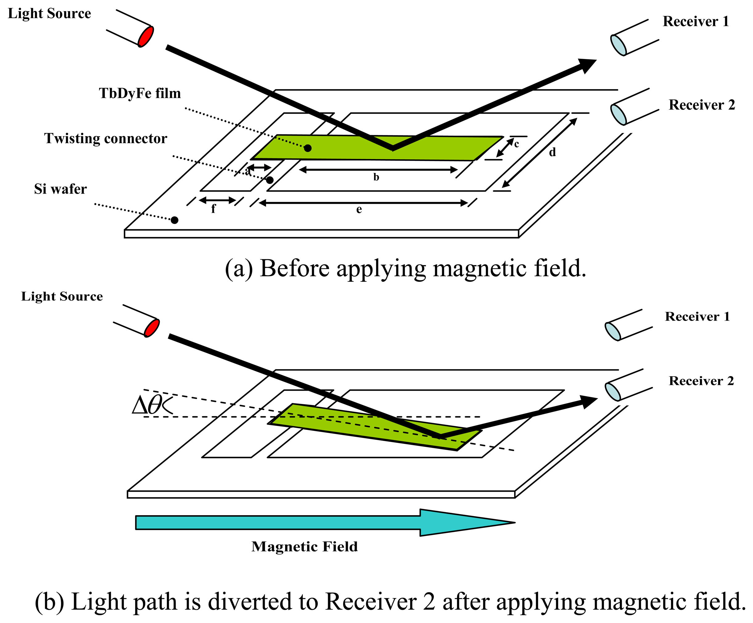
2.1. Optical Switch Design

The schematic diagram of an optical mirror and switch design is illustrated in Figure 1. The optical switch consists of a micro mirror and twisting connectors with frame for bending of mirror (size of a: 600μm, b: 4mm, c: 800μm, d: 2mm, e: 5mm, f: 1.5mm). And all of the structures are fabricated from Si thin wafer of 50μm thickness.
Outside of the device, one light source and two receivers are arranged for switch matrix. Optical laser is used as a light source and position sensitive detector is used as receivers. The upper surface of the cantilever is deposited with magnetostrictive TbDyFe film for positive magnetostriction. This film-coated surface can be used as micro mirror by itself. When the magnetic field is applied to the TbDyFe film deposited mirror along the longitudinal direction (Figure 1(b)), magnetic field creates a magnetization in the deposited film that generates magnetostriction. Magnetostriction is the change in shape and size of a body when its state of magnetization is changed by a magnetic field. Magnetization induces strains and it makes a bending angle of the optical mirror. From the mechanism, the light path can be changed according to the bending angle from receiver 1 to receiver 2 (Figure 1(b)). The amount of deflected angle can be controlled by the deposited film thickness and the magnitude of external magnetic field.

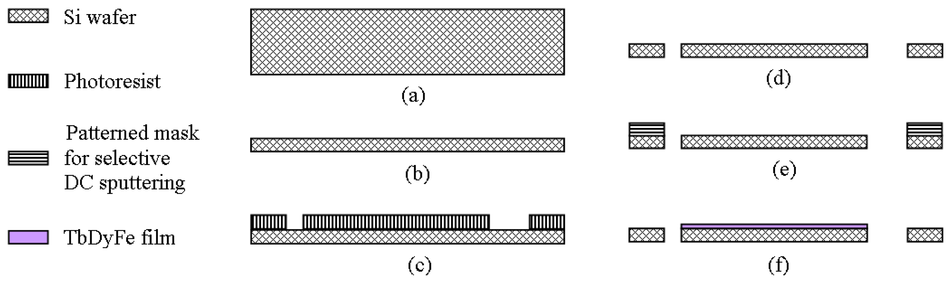
2.2. Fabrication Process for Magnetostrictive Mirror

To make a suggested optical switch design, the micromachining process is combined with selective DC magnetron sputtering techniques. The fabrication sequence of the magnetostrictive mirror is shown in Figure 2. The process starts on the thick Si wafer of 750μm thickness (Figure 2(a)), and it is dry etched to reduce its thickness to 51∼52μm.
After the etching process, the thin Si wafer is put to the polishing process for fine surface roughness (Figure 2(b)). Then, a thick photoresist (Shipley SJR 5740) is spun on the thin Si wafer with a spin speed of 1100rpm for 15 seconds (yielding a final thickness of approximately 30μm), and patterned to act as empty holes for the designed shape (Figure 2(c)). The Si wafer thickness of 50μm is anisotropically etched by RIE (Reactive Ion Etching) to create holes for a cantilever beam, twisting connectors and a frame structure. After removing the photoresist layer (Figure 2(d)), the outside of the cantilever beam is covered with mask for selective DC magnetron sputtering (Figure 2(e)). The covered area should include the upper surface of the twist connector. Only the cantilever part should be exposed. For the verification of thickness effect, three samples are prepared by depositing TbDyFe thin films of thickness 0.5μm, 1μm, and 2μm, respectively, on the cantilever part using TbDyFe composite target. Ar gas below 1.2×10⁻⁹ torr and DC input power of 180W are used for the sputtering process. During the sputtering process the substrate holder is heated to 300°C to get fine grains. After the film deposition, the mask is removed (Figure 2(f)). The fabricated structure of TbDyFe film deposited mirror is shown in Figure 3.

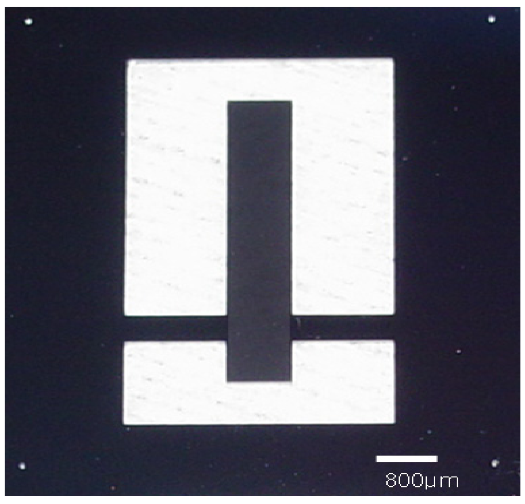
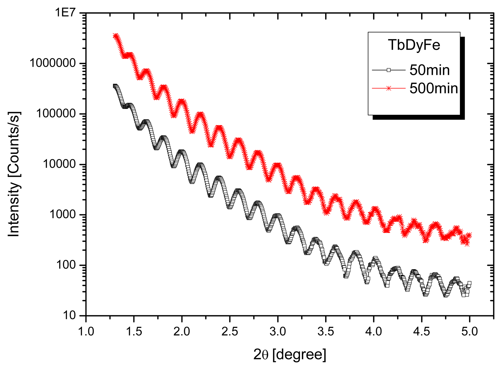
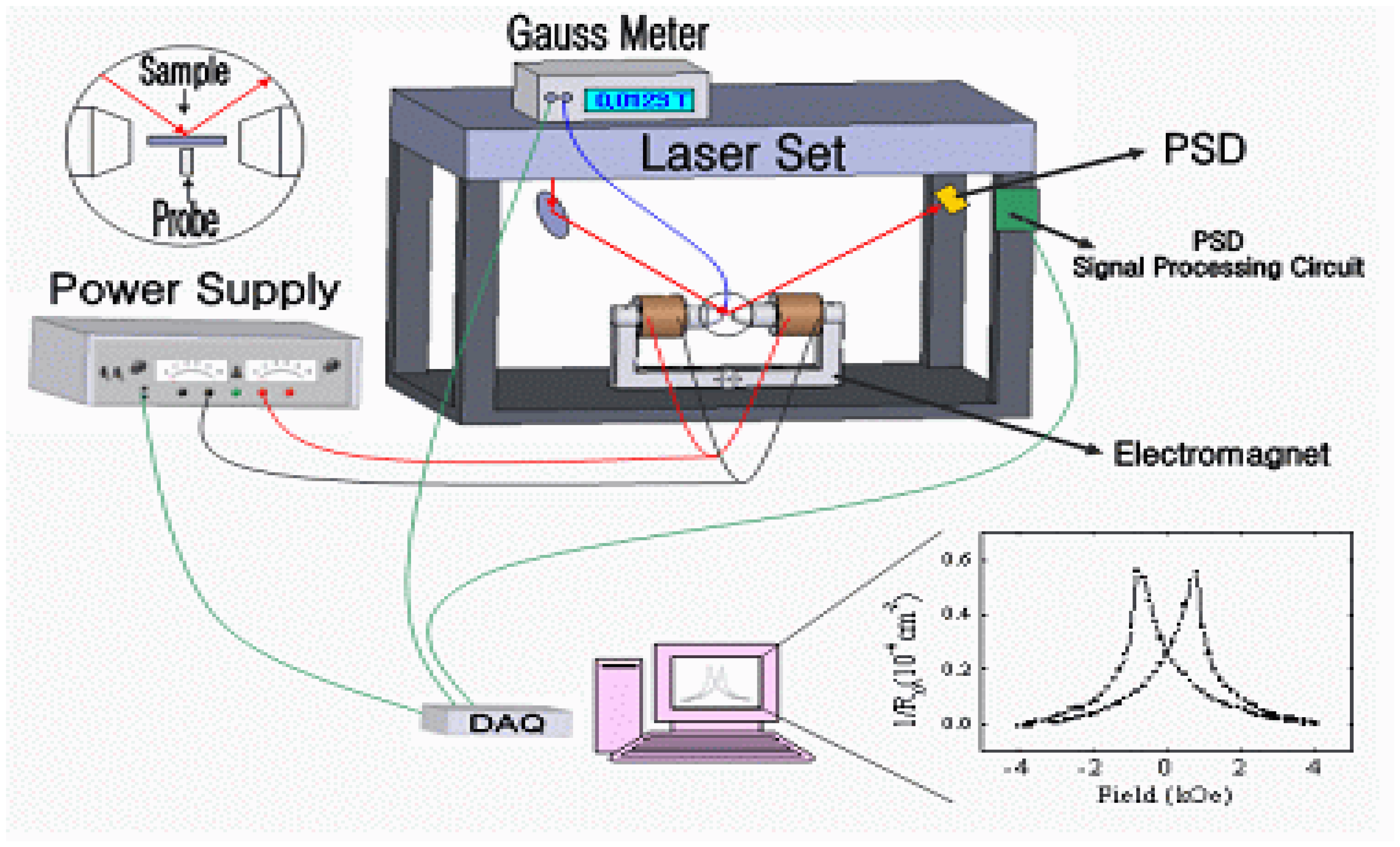
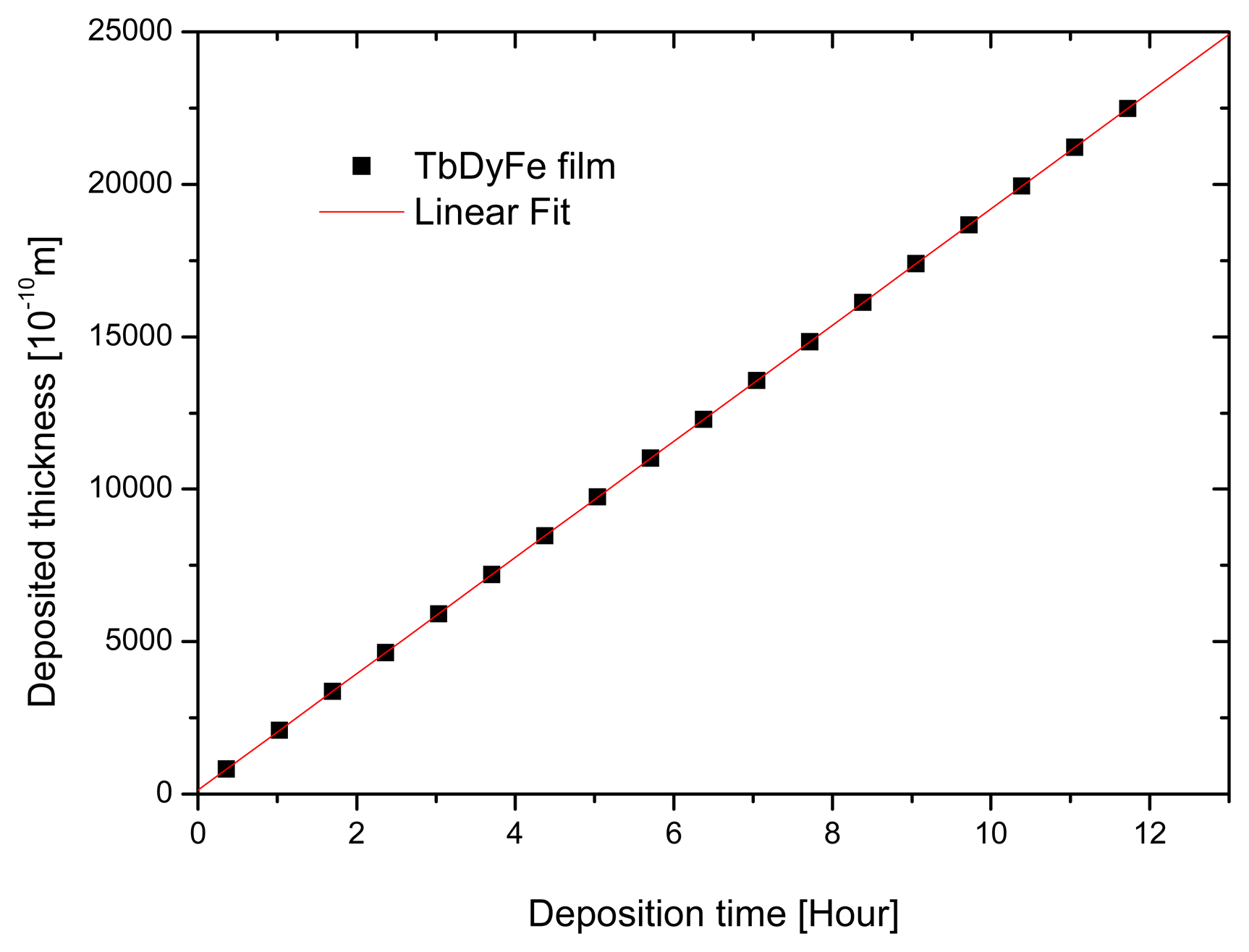
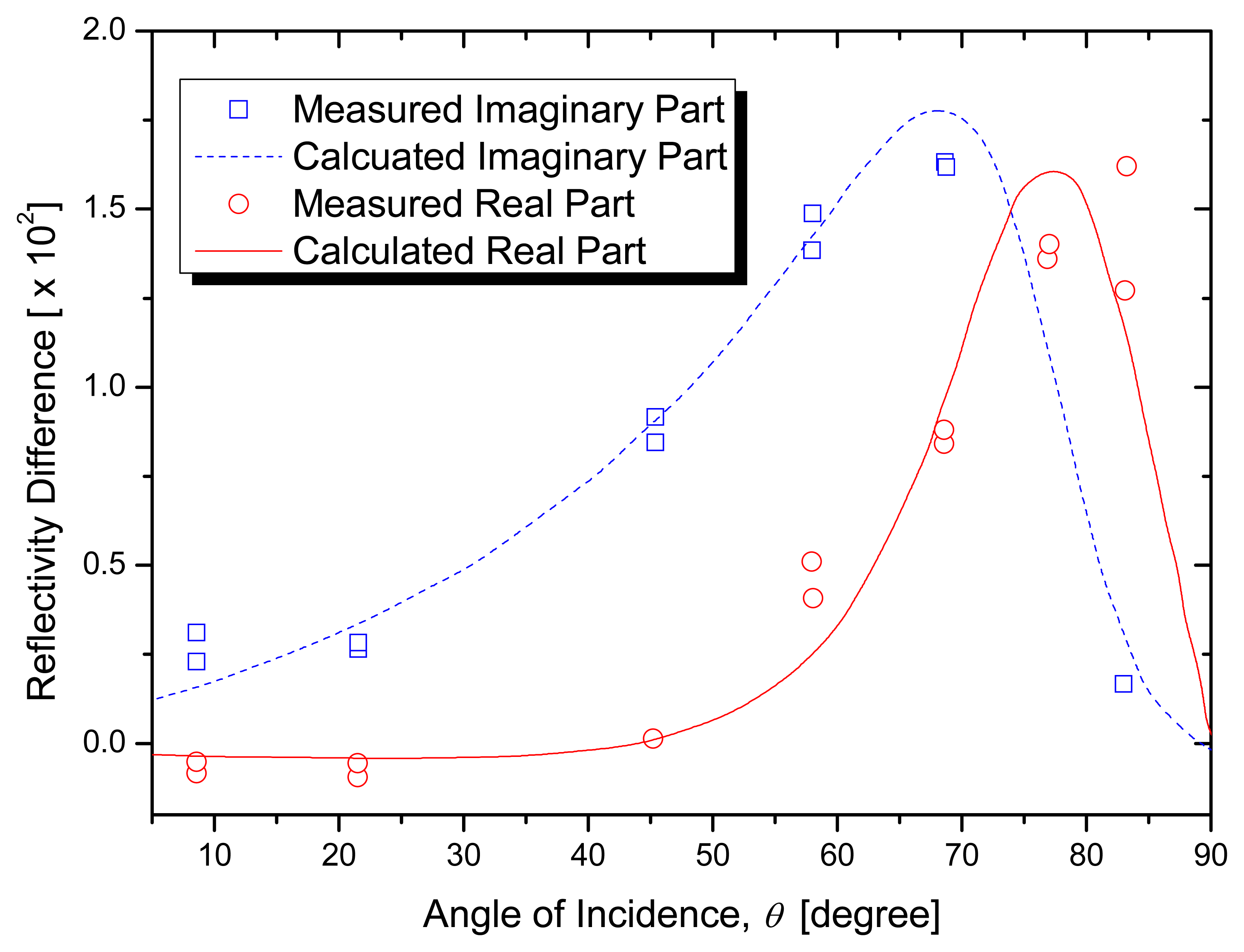
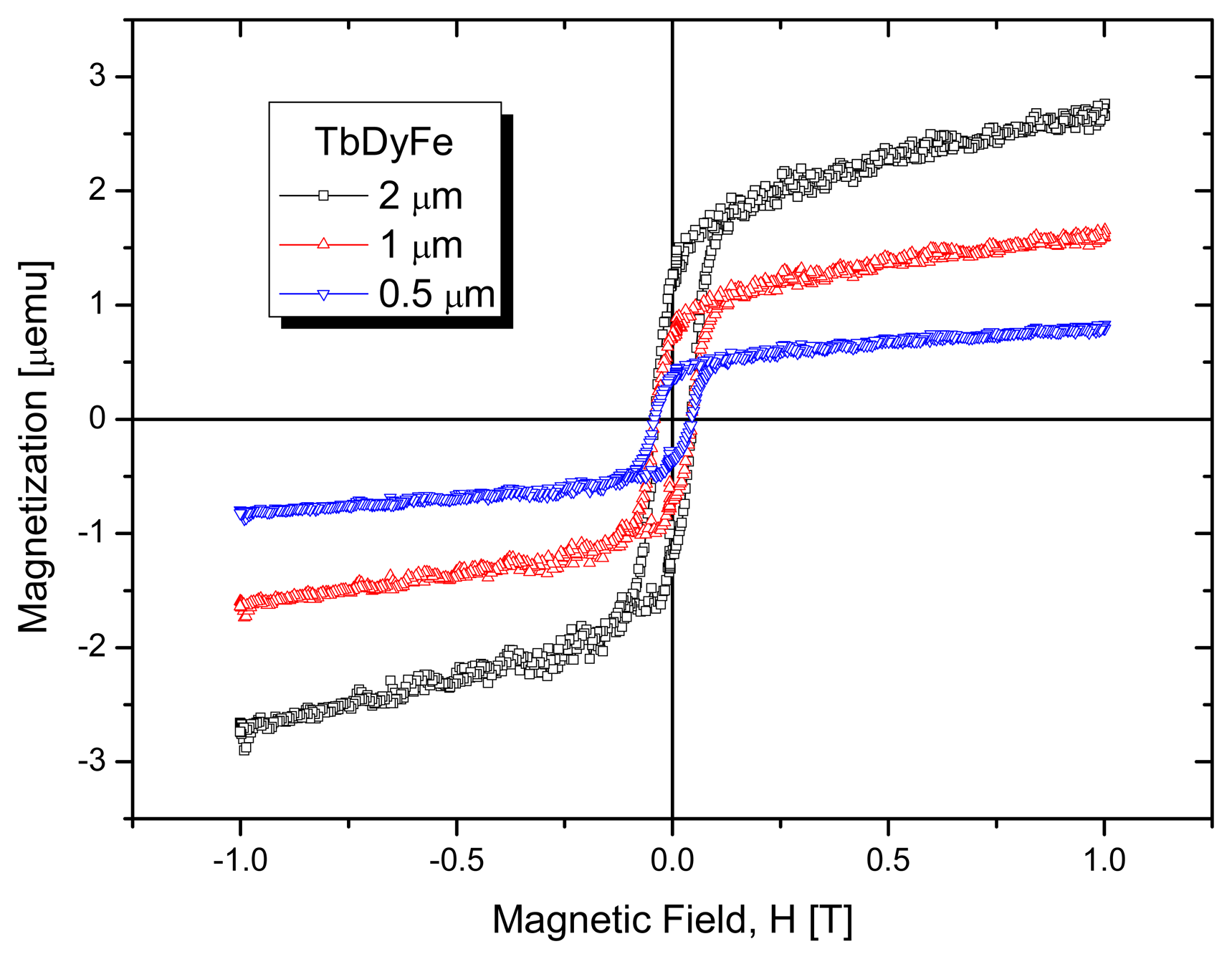
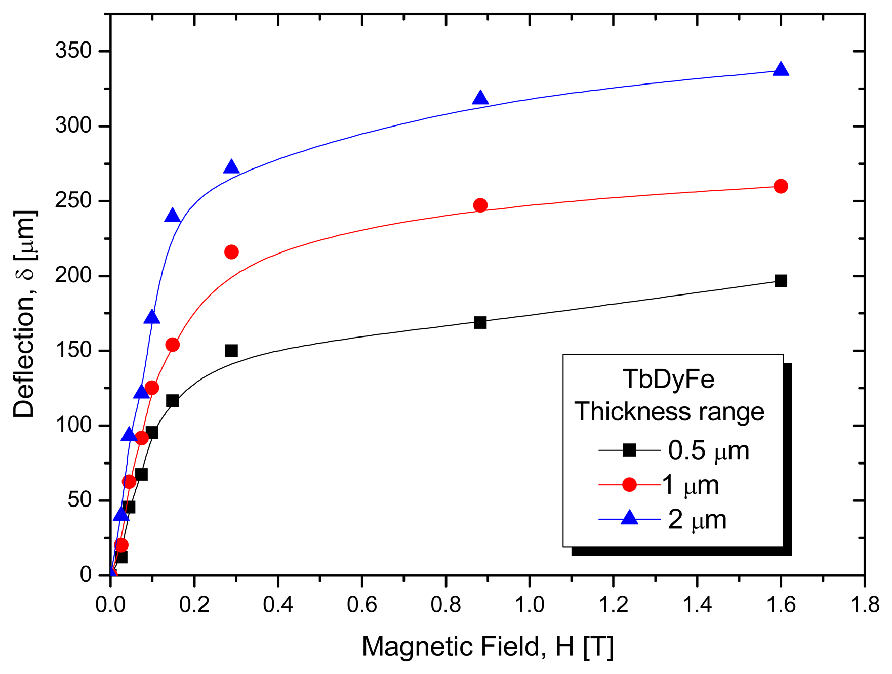
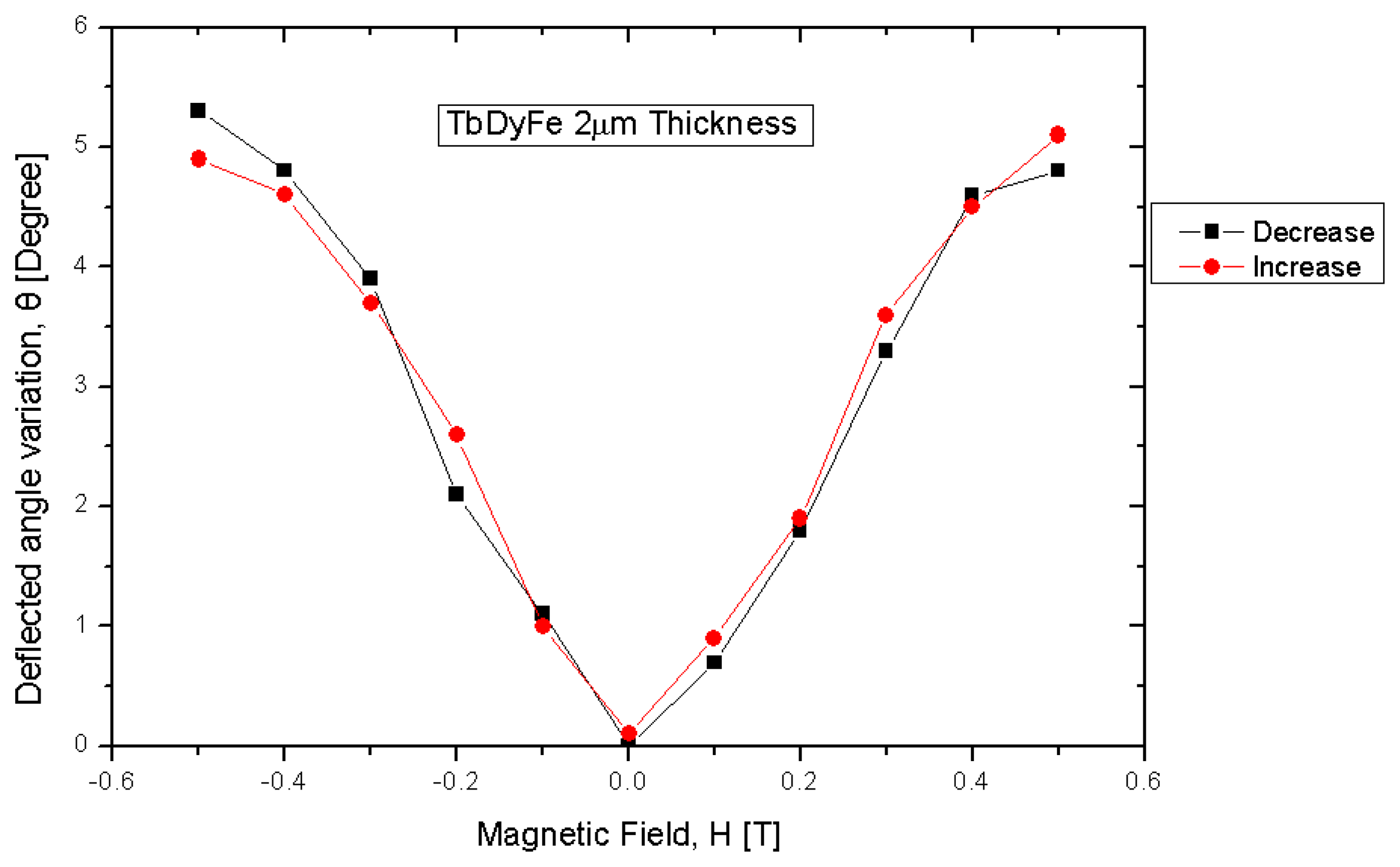
3. Measurement and Characterization Results

The characteristics of fabricated mirror depend on the thickness of the deposited TbDyFe film and magnitude of applied external magnetic field. After the film deposition, the film thicknesses are measured by X-ray diffraction (XRD).
Figure 4 shows the measured X-ray diffraction of TbDyFe films in terms of the diffraction angle-intensity (θ-I) relation. From the figure, the film thicknesses can be calculated as follows [8]:
Λ = I λ ( 2 sin 2 θ 2 δ ) .
where, I is the intensity of the upper peak point at each 2θ, λ is the X-ray wave length of TbDyFe film, Λ is the film thickness, and δ is the real part of the refractive index and has a value of 10-5. Λ can be obtained by fitting θ-I under the condition of the positive least value of δ. It presents the deposited thicknesses as a function of deposition time. The thickness calculated results are presented in Figure 5. Under the suggested sputter conditions, it takes about 12 hours to deposit 2μm thickness TbDyFe film.
The most sensitive form of ellipsometry is the oblique-incidence reflectivity difference (OI-RD) technique [10]. It is a polarization-modulated nulling ellipsometry that directly measures the difference in fractional reflectivity change. To relate the structural and kinetic information on a thin film or the modified surface layer on a substrate to the experimentally measured optical response and to reach the full potential of the OI-RD technique, one typically resorts to mean-field models of optics for multilayer films [11]. Using a classical multi-layer model to describe the optical response from the surface of a homogeneous substrate covered with a thin film, Zhu and co-workers have shown the fractional reflectivity change ΔReflectivity as the Equation (2) [12,13].
Δ Re flectivity i [ 4 π ε s tan 2 θ cos θ ε 0 1 / 2 ( ε s ε 0 ) ( ε s / ε 0 tan 2 θ ) ] × ( ε d ε 0 ) ( ε d ε 0 ) ε d ( d λ L ) .
where, θ is the incidence angle of the sample; ε0, εd, and εs are the optical dielectric constants of the ambient, the thin film, and the substrate, respectively; d is the thickness of the film (or the modified surface layer), λL is the He-Ne probe laser wave length. Changes at the surface other than thickness, such as mass density, chemical makeup, and morphology, are represented by the corresponding change in εd. The optical arrangement and experimental procedures for obtaining fractional reflectivity changes have been described in detail by Thomas et al. [10].
In Figure 6, we display reflectivity difference in response to adsorption of one monolayer of TbDyFe of 0.5μm thickness on Si substrate versus the incidence angle.
We have computed reflectivity difference by using Equation (1). The calculated incidence-angle dependence agrees quantitatively with the experimental data.
The magnetization and the magnetostrictions are also measured to characterize the magnetic properties of the TbDyFe mirror. The magnetization of the mirror under the external magnetic field is observed using VSM (Vibrating Sample Magnetometer). Figure 7 shows the measured magnetization. Magnetization values increase with the increase of deposited TbDyFe film thickness although coercive force at each thickness shows almost same value. Magnetostriction is the changing of a material's physical dimensions in response to changing its magnetization. In other words, a magnetostrictive material will change shape when it is subjected to a magnetic field. Most ferromagnetic materials exhibit some measurable magnetostriction. The magnetostriction of the mirror is determined by measuring differences of the curvature of the film coated cantilever beam using an optical cantilever method. The curvatures of the length and width directions of the mirror due to external magnetic fields are measured by detecting deflected laser signals through a position sensitive detector. The measurement set up for magnetostriction is illustrated in Figure 8.
The measured curvatures are converted into magnetostrictions as follows [14]:
Magntostriction = t s 2 Y s 9 t f Y f ( 1 + ν f ) ( 1 + ν s ) ( 1 R L 1 R w ) .
where, Y is Young's modulus, ν is Poisson's ratio, t is thickness, R is the radius of curvature, and the subscript s and f denote the value for substrate and film, respectively. Since the deflection is proportional to the amount of magnetostriction, the magnetostriction can be calculated using the deflection. The measured results of the magnetostriction are shown in Figure 9. From the figure, it can be seen that the deflection amounts increase with increasing TbDyFe film thicknesses; and the maximum measured deflection is about 330μm when the film thickness is 2μm.
And, the magneto-optical characteristics are determined by measuring the deflected angles of the emitted light under the variation of the magnitude of applied magnetic field. Figure 10 shows the magneto-mechanical characteristics of the fabricated magnetostrictive mirror in terms of magnetic field and deflected angle variations when the TbDyFe film thickness is 2μm. To investigate the defection characteristics of the fabricated mirror, two curves are obtained by increasing and decreasing the applied magnetic field amounts. Also, it can be seen that the two curves show very similar deflection trends under same magnetic field variations.

4. Conclusions

A magnetostrictive optical mirror and switch design is proposed and investigated in this study. For the fabrication of the mirror design, the micromachining technique is combined with the selective DC magnetron sputter-deposition technique. The magnetic and the magneto-optical characteristics have been investigated for the application of fabricated TbDyFe mirror. To ensure deposited rate, XRD patterns are examined and magnetization of the mirrors at each thickness are obtained and reflectivity difference is analyzed through experimental and numerical method. At low magnetic field the strain is linear, but it becomes nonlinear at higher magnetic field. In this process, the magnitude of the magnetization within a domain did not changed appreciably; only its orientation with respect to local crystal axes has been altered. Above the low magnetic field levels, where the domains have completely shifted, the intrinsic magnetization is changed which contributes to the transitional knee. The maximum deflection of the mirror at the end point is about 330μm; and the maximum deflected angle change is about 5.3° for the fabricated mirror of 2μm thickness.

Acknowledgments

This work was supported by Inha University.

References and Notes

  1. Tomic, M.C.; Elazar, J.M.; Djinovic, Z.V. Voltage measurement based on the electrostrictive effect with simultaneous temperature measurement using a 3 × 3 fiber-optic coupler and low coherence interferometric interrogation. Sens. Actuator A-Phys. 2004, 115, 462–469. [Google Scholar]
  2. Životský, O.; Postava, K.; Kraus, L.; Foldyna, M.; Pištora, J. Magnetic and magneto-optical properties of CoFeCrSiB amorphous ribbons. J. Magn. Magn. Mater. 2006, 304, e534–536. [Google Scholar]
  3. Sánchez, L.J.L.; Sánchez, V.C.F.; Santana, G.A. Hard magnetic properties of isotropic nanostructured Y0.5Pr0.5Co5 powders. J. Magn. Magn. Mater. 2005, 294, 226–231. [Google Scholar]
  4. Guoa, Y.Q.; Li, W.; Luo, J.; Feng, W.C.; Liang, J.K. Structure and magnetic characteristics of novel SmCo-based hard magnetic alloys. J. Magn. Magn. Mater. 2006, 303, e307–e370. [Google Scholar]
  5. Rizal, C.S. Study of magnetic anisotropy and magnetoresistance effects in ferromagnetic Co/Au multilayer films prepared by oblique incidence evaporation method. J. Magn. Magn. Mater. 2007, 310, e646–e648. [Google Scholar]
  6. Cho, C.; Lee, H.S.; Kim, C.B.; Beom, H.G. A Finite Element Analysis for Magnetostrictive Thin Film Structures and its Experimental Verification. Key Eng. Mater. 2006, 306-308, 1151–1156. [Google Scholar]
  7. Speliotis, A.; Kalogirou, O.; Vouroutzis, N.; Niarchos, D. Magnetostrictive properties of amorphous and nanocrystalline TbDyFe flms with Nb and Zr additives. J. Magn. Magn. Mater. 1998, 187, 17–22. [Google Scholar]
  8. Lee, H.S.; Cho, C.; Chang, S.P. Effect of SmFe and TbFe film thickness on magnetostrictions for MEMS devices. J. Mater. Sci. 2006, 42, 384–388. [Google Scholar]
  9. Body, C.; Reyne, G.; Meunier, G.; Quandt, E.; Seemann, K. Application of magnetostrictive thin films for microdevices. IEEE Trans. Magn. 1997, 33, 2163–2166. [Google Scholar]
  10. Thomas, P.; Nabighian, E.; Bartelt, M.C.; Fong, C.Y.; Zhu, X.D. An oblique-incidence optical reflectivity difference (OI-RD) and LEED study of rare gas growth on a lattice-mismatched metal substrate. Appl. Phys. 2004, A79, 131–137. [Google Scholar]
  11. McIntyre, J.D.E.; Aspnes, D.E. Differential reflection spectroscopy of very thin surface films. Surf. Sci. 1971, 24, 417–434. [Google Scholar]
  12. Wong, A.; Zhu, X.D. An optical differential reflectance study of adsorption and desorption of xenon and deuterium on Ni(111). Appl. Phys. 1996, A63, 1–8. [Google Scholar]
  13. Zhu, X.D. Oblique-incidence optical reflectivity difference from a rough film of crystalline material. Phys. Rev. 2004, B69, 115407-1–5. [Google Scholar]
  14. Sander, D. The correlation between mechanical stress and magnetic anisotropy in ultrathin films. Rep. Prog. Phys. 1999, 62, 809–858. [Google Scholar]
Figure 1. Schematic models of magnetostrictive optical switch matrix.
Sensors 07 02174f1
Figure 2. Micromachining and TbDyFe thin film deposition sequences for the fabrication of magnetostrictive micro mirror.
Sensors 07 02174f2
Figure 3. Fabricated magnetostrictive micro mirror.
Sensors 07 02174f3
Figure 4. X-ray diffraction for thickness measurement with deposition time.
Sensors 07 02174f4
Figure 5. Converted thickness results with deposition time from Equation 1.
Sensors 07 02174f5
Figure 6. Reflectivity differences in response to TbDyFe film of 0.5μm thickness on Si substrate versus the incidence angle. The results are calculated using Equation (2).
Sensors 07 02174f6
Figure 7. Magnetization of TbDyFe mirror at each film thickness.
Sensors 07 02174f7
Figure 8. Measurement set up for magnetostriction.
Sensors 07 02174f8
Figure 9. Magnetostriction and magneto-mechanical characteristics: Effects of the thicknesses of the TbDyFe film on the mirror deflections.
Sensors 07 02174f9
Figure 10. Magnetostriction and magneto-optical characteristics: Deflected light angle changes under magnetic field.
Sensors 07 02174f10

