Modeling and Fabrication of Micro FET Pressure Sensor with Circuits

Department of Mechanical Engineering, National Chung Hsing University, 250 Kuo-Kuang Rd., Taichung, 402 Taiwan
*
Author to whom correspondence should be addressed.
Sensors 2007, 7(12), 3386-3398; https://doi.org/10.3390/s7123386
Submission received: 19 November 2007
/
Accepted: 18 December 2007
/
Published: 19 November 2007
(This article belongs to the Special Issue Modeling, Testing and Reliability Issues in MEMS Engineering)
Abstract
:This paper presents the simulation, fabrication and characterization of a micro FET (field effect transistor) pressure sensor with readout circuits. The pressure sensor includes 16 sensing cells in parallel. Each sensing cell that is circular shape is composed of an MOS (metal oxide semiconductor) and a suspended membrane, which the suspended membrane is the movable gate of the MOS. The CoventorWare is used to simulate the behaviors of the pressure sensor, and the HSPICE is employed to evaluate the characteristics of the circuits. The pressure sensor integrated with circuits is manufactured using the commercial 0.35 μm CMOS (complementary metal oxide semiconductor) process and a post-process. In order to obtain the suspended membranes, the pressure sensor requires a post-CMOS process. The post-process adopts etchants to etch the sacrificial layers in the pressure sensors to release the suspended membranes, and then the etch holes in the pressure sensor are sealed by LPCVD (low pressure chemical vapor deposition) parylene. The pressure sensor produces a change in current when applying a pressure to the sensing cells. The circuits are utilized to convert the current variation of the pressure sensor into the voltage output. Experimental results show that the pressure sensor has a sensitivity of 0.032 mV/kPa in the pressure range of 0-500 kPa.
1. Introduction
Micro pressure sensors that are important components can be applied in biomedical and various industries. For instance, a micro capacitive pressure sensor, presented by Eggers et al. [1], was utilized in the biomedical measurement. Huang et al. [2] fabricated a piezoelectric pressure sensor to monitor the instant pressure variation of the molding injection. Berns et al. [3] developed a micro pressure sensor array to measure the wall pressure in turbulent flows. A silica fiber optic pressure sensor, proposed by Pulliam et al. [4], was applied in high-temperature propulsive environments.
Recently, microelectromechanical system (MEMS) technology has been applied to fabricate various micro devices. The advantages of micro pressure sensors manufactured by MEMS technology are small size, high performance and easy mass-production. Several micro pressure sensors [5-10] have been fabricated using MEMS technology. For instance, Lin et al. [5] employed a surface micromachining process to manufacture a piezoresistive pressure sensor, in which the polysilicon diaphragms were deposited by LPCVD. The pressure sensor had a sensitivity of 0.15 mV/psi. A piezoresistive pressure sensor, proposed by Wu et al. [6], was made using a bulk micromachining process. The piezoresistors were the single-crystalline 3C-SiC film grown by APCVD (atmospheric pressure chemical vapor deposition), and the diaphragm was released using an anisotropic etching of KOH solution. The sensitivity of the pressure sensor was 177.6 μV/psi at room temperature. Dai et al. [7] presented a capacitive pressure sensor fabricated by the CMOS process, in which the membranes were released using an anisotropic dry etching and a wet etching, and the etch holes were sealed by PECVD (plasma enhanced chemical vapor deposition) nitride. Sippola et al. [8] reported a ceramic capacitive pressure sensor produced by a thick film screen-printing technique. The pressure sensor comprised a top electrode deposited on a ceramic diaphragm and a bottom electrode deposited on an alumina substrate, and the ceramic cavity and diaphragm were created using a thick film sacrificial layer. The pressure sensor had a sensitivity of 9.2 fF/psi. An FET pressure sensor, reported by Svensson et al. [9], was fabricated by a surface micromachining process. The pressure sensor was an MOS transistor where the membrane was the device gate, and the two silicon diffusions under the membrane were the source and the drain regions. The sensitivity of the FET pressure sensor was 0.1 mA/bar. Hynes et al. [10] manufactured an FET pressure sensor using a surface micromachining process, in which a sacrificial oxide layer and a polysilicon diaphragm were deposited on the pressure sensing area, and then HF was used to etch the sacrificial oxide from beneath the polysilicon diaphragm. The cavity was sealed with LPCVD oxide. The FET pressure sensor had a sensitivity of 1.3 μA/psi.
Micro pressure sensors, proposed by Lin et al. [5], Wu et al. [6], Sippola et al. [8], Svensson et al. [9] and Hynes et al. [10] without integration with circuits on a chip, had the disadvantages of high packaging cost and large chip area. The aim of this work is to manufacture an FET pressure sensor with circuits on a chip. The advantages of the integrated FET pressure sensor are low packaging cost, small chip area, and high sensitivity. The CMOS-MEMS [11-13] technique is the use of commercial CMOS process to fabricate MEMS devices. The benefit of micro pressure sensors manufactured by the CMOS-MEMS technique is the capability of integration with readout circuits as a system on chip (SOC). In this work, we employ the CMOS-MEMS technique to fabricate an FET pressure sensor integrated with readout circuits on a chip. The fabrication of the pressure sensor in this work is easier than that of Svensson et al. [9] and Hynes et al. [10]. The FET pressure sensor is constructed by 16 sensing cells in parallel, and each sensing cell consists of a suspended membrane and an NMOS. When applying a pressure to the sensing cells, the pressure sensor generates a change in current. The readout circuits are employed to convert the current variation of the pressure sensor into the voltage output. In order to release the membranes, the pressure sensor needs a post-CMOS process. The post-process is the use of wet etching to remove the sacrificial layers, and to obtain the suspended membrane. A LPCVD parylene is utilized to seal the etch holes in the pressure sensor. Experimental results reveal that the sensitivity of the FET pressure sensor is 0.032 mV/kPa in the pressure range of 0-500 kPa.
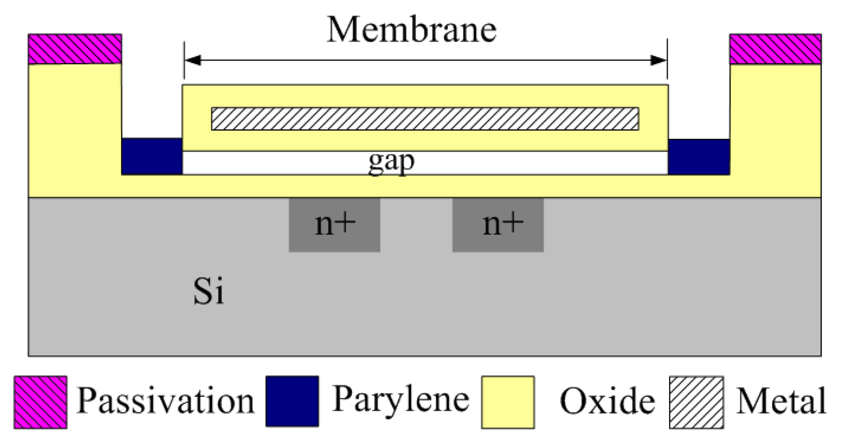
2. Structure of Pressure Sensor
Figure 1 shows the layout of the FET pressure sensor integrated with readout circuits on a chip. The pressure sensor consists of 16 sensing cells in parallel. All sensing cells that are circular shape have the same dimensions. Figure 2 illustrates the schematic cross-sectional view of a sensing cell, which is composed of a suspended membrane and an NMOS. The suspended membrane is the gate of the NMOS, and the two silicon diffusions under the membrane are the source and drain regions. The diameter of each sensing cell is 100 μm. The membrane is a sandwiched structure that contains silicon dioxide, metal and silicon oxide layers, in which the metal layer is the electrode and each layer has a thickness of about 1 μm. The gap between the membrane and the substrate is about 0.65 μm. As shown in Fig. 2, the dielectric of the NMOS consists of a 1 μm oxide layer, a 0.65 μm air gap and a 1 μm oxide layer. The structure can be taken as a series of three capacitors and the total capacitance pre unit area Ct can be expressed as,
where Cgap and Cox represent the individual capacitance per unit area of the air gap and oxide, respectively. The membrane generates a deformation when applying a uniform pressure to the sensing cell, leading to the total capacitance of the NMOS changes. In the saturation region, the drain current, Ids, of the NMOS can be expressed as [10],
where L represents the channel length of the NMOS, W is the channel width of the NMOS, Ct is the total capacitance of the NMOS, μn is the mobility of the electrons, Vt is the threshold voltage and Vgs is the gate-to-source voltage. According to Eq. (2), the drain current, Ids, changes as the capacitance, Ct, varies. Therefore, the FET pressure sensor produces a change in current upon applying a pressure to the membranes of the sensing cells.
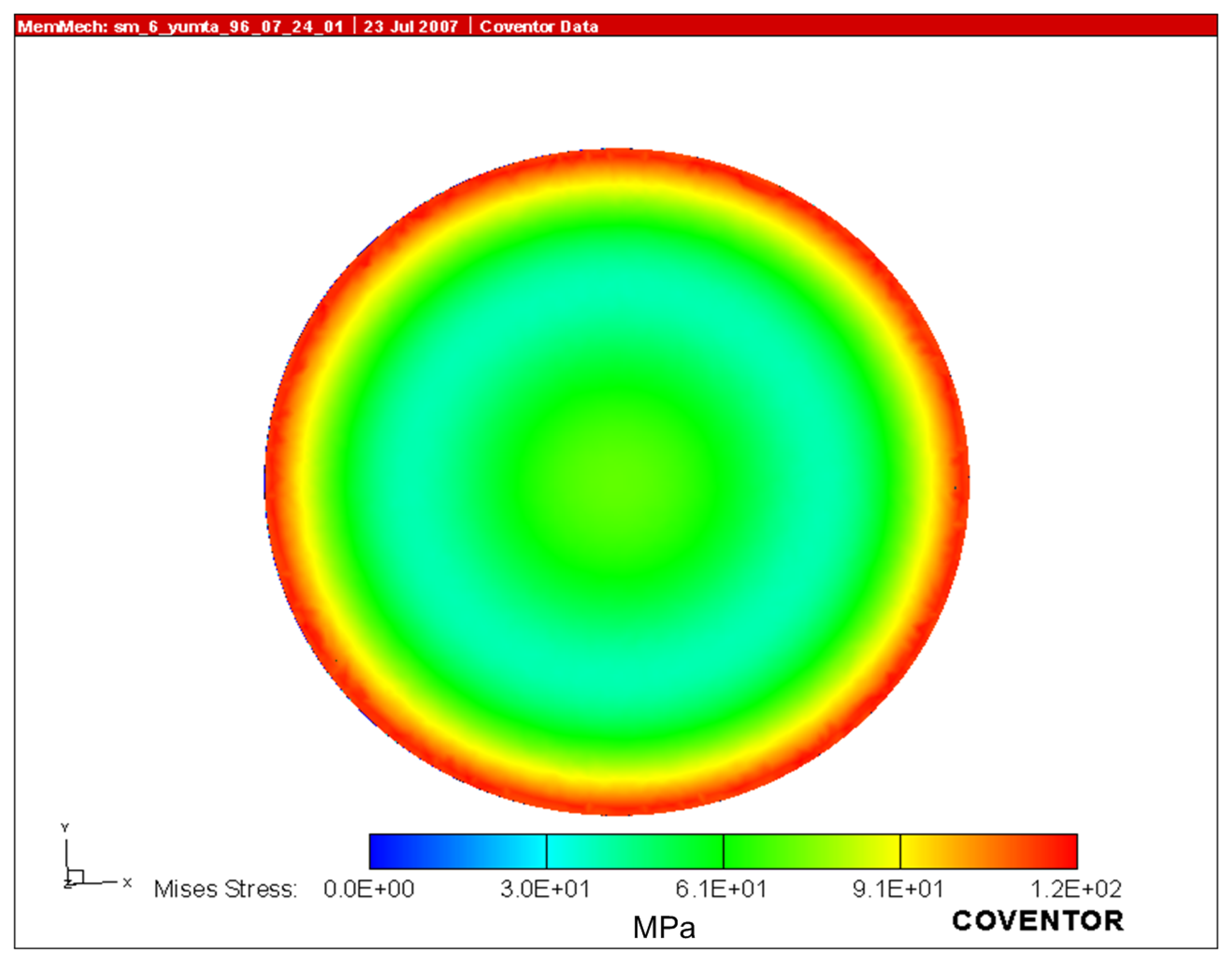
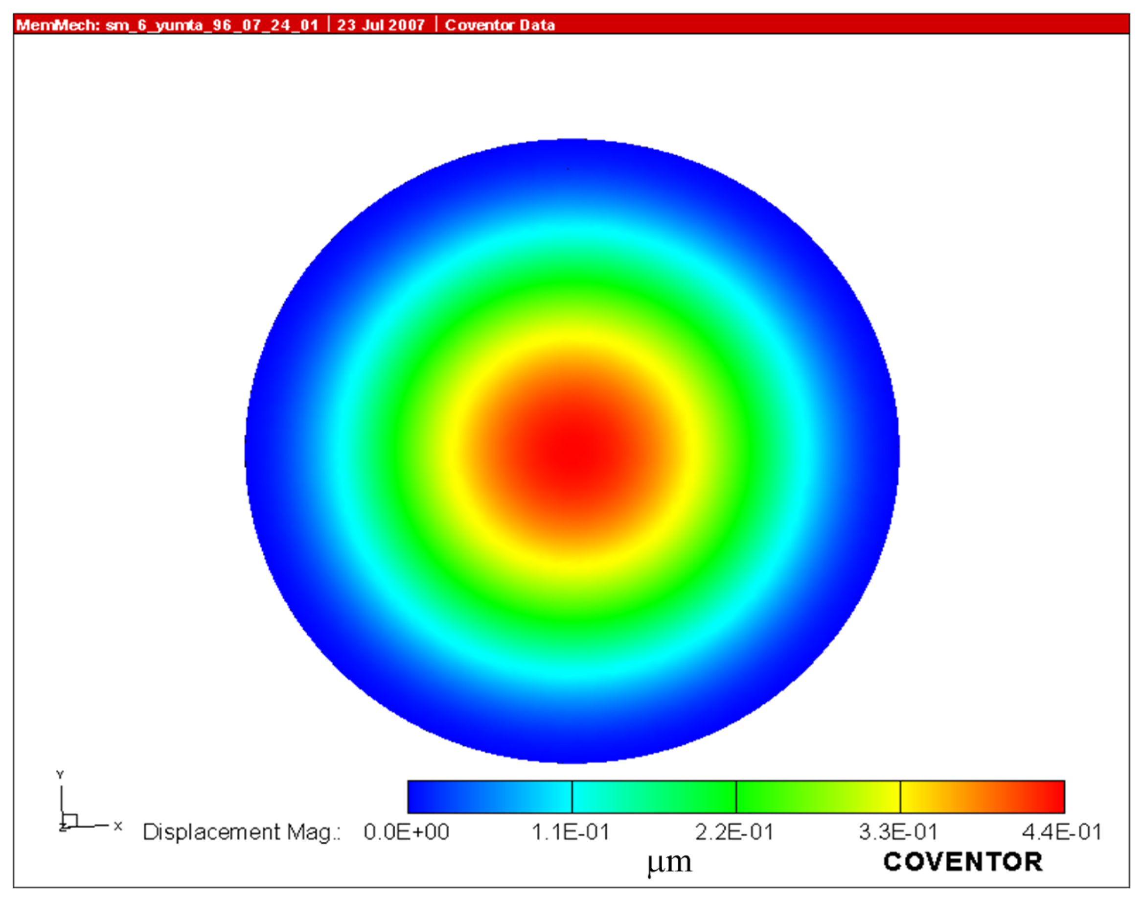
The finite element method software, CoventorWare, is utilized to simulate the behaviors of the FET pressure sensor. The model of only one sensing cell is constructed because all sensing cells are the same. The triangular elements are employed to mesh the model. The materials of the membrane are aluminum (Young's modulus of 70 GPa, Poisson's ratio of 0.3 and mass density of 2679 kg/m3) and silicon dioxide (Young's modulus of 69 GPa, Poisson's ratio of 0.17 and mass density of 2200 kg/m3) [10]. The boundary condition is that the membrane edge is fixed, and the load is a uniform pressure applied to the membrane. The stress and displacement of the membrane can be computed through the simulation. Figure 3 presents the stress distribution of the membrane at a pressure of 500 kPa. The simulated result shows that the maximum stress situates at the edge of the circular membrane. Figure 4 shows the displacement of the membrane in the sensing cell at a pressure of 500 kPa. The maximum displacement is located at the center of the membrane. The relation between the pressure and displacement at the center of the membrane is shown in Fig. 5. The result depicts that the displacement at the center of the membrane is about 0.44 μm at a pressure of 500 kPa. The transverse displacement of a clamped circular thin plate can be expressed as [7, 15],
where p represents uniform distributed load, D is the flexural rigidity of the plate and a is the radius of the plate. Substituting P=500 kPa, a=50 μm, h=2.65 μm and r=0 into Eq. (3), we obtain that the displacement at the center of the circular plate is about 0.41 μm, and the value approximates to the simulated result of 0.44 μm.
The professional circuit simulation software, HSPICE, is utilized to simulate the current-to-voltage characteristics of the FET pressure sensor and the output voltage of the readout circuits. Figure 6 presents the simulated results of Ids/ Vds output characteristics for the FET pressure sensor. As shown in Fig. 6, the current of Ids depended on the voltages of Vgs and Vds, and the current of Ids is about 1.5 mA at Vgs=3 V, Vds>1.5 V. Figure 7 illustrates the readout circuits with an operational amplifier that are used to convert the current variation of the FET pressure sensor into the voltage output. As shown in Fig. 7, R1, R2, R3, R4 and R5 represent the resistances, Ms is the sensing MOS of the pressure sensor, Vdd is a voltage power supply, and Vout is the output voltage. Figure 8 shows the design of the operational amplifier circuit, where Vdd represents a voltage power supply and Vss is the ground. Figure 9 depicts the simulated results of the frequency response for the operational amplifier. The dc open loop gain of the operational amplifier is approximately 93 dB, and the phase margin of the operational amplifier is about 80°. Figure 10 displays the simulated output voltage of the readout circuits. In this simulation, the resistances R1, R2, R3, R4, and R5 are set with 0.1, 1, 10, 0.1, and 0.1 kΩ, respectively. The Vdd and Vgs voltages are given by a voltage of 3.3 V and 3 V, respectively. The Ids current of the pressure sensor is set to change from 1560 to 1585 μA. The simulated result shows that the output voltage changes from 1085 to 1065 mV as the current of the pressure sensor varies from 1560 to 1585 μA.
3. Fabrication of Pressure Sensor
The commercial 0.35 μm CMOS process of Taiwan Semiconductor Manufacturing Company (TSMC) is employed to fabricate the FET pressure sensor integrated with readout circuits. Figure 11 displays the process flow of the FET pressure sensor with circuits. Figure 11(a) shows the schematic cross-section of the pressure sensor after the CMOS process. In the pressure sensor, the membranes are composed of the oxide, metal and oxide layers. The etch holes are filled with metal and via layers, which the materials of the metal and via layers are aluminum (Al) and tungsten (W), respectively. The metal layer under the membrane and the Al and W layers in the etch holes are the sacrificial layers. In order to obtain the suspended membranes, the FET pressure sensor needs a post-CMOS process to remove the sacrificial layer. The post-process used wet etching to etch the sacrificial layers, and to release the suspended membranes. Figure 11(b) displays that the pressure sensor is immersed in two etchants: one is an Al etchant with phosphoric acid, nitric acid, acetic acid and DI water in the ratio 14:1:2:3 and the other is a W etchant with sulfuric acid and hydrogen peroxide in the ratio 2:1. The sacrificial layers are removed and the suspended membranes are released, which an air gap between the membrane and substrate is formed. Figure 12 shows the photograph of the FET pressure sensor with readout circuits on a chip after the wet etching process. Figure 13 depicts a scanning electron microscopy (SEM) image of the FET pressure sensor after the wet etching process. A white light interferometer (Zoomsurf 3D from Fogale Nanotech Co.) is utilized to measure the flatness of the membranes. The result shows that the maximum deflection of the membranes is about 0.06 μm. The etch holes in the pressure sensor have to be sealed. Figure 11(c) shows that the etch holes are sealed using a LPCVD parylene, and the paraylene film is patterned by a dry etching. The thickness of the parylene film is about 1.6 μm. The FET pressure sensor that the cavities are nearly at vacuum is an absolute pressure sensor due to the LPCVD parylene is processed in a high vacuum chamber.
4. Results and Discussion
The FET pressure sensor was mounted in a pressure chamber. The nitrogen pressure source was supplied to the pressure chamber, and the nitrogen pressure in the chamber could be tuned through the gas valves. A calibrated pressure sensor was utilized to monitor the gas pressure in the pressure chamber. The power supply provided the Vgs and Vds (drain-to-source voltage) voltages of the FET pressure sensor. The output current of the FET pressure sensor without the readout circuits was detected using the digital multimeter. Figure 14 reveals the measured results of Ids/Vds output characteristics for the FET pressure sensor. In the measurement, the FET pressure sensor was tested at different Vgs (from 0 to 5 V) and Vds (from 0 to 3.3 V) voltages without pressure in the pressure chamber. The experimental results of Ids/Vds characteristics for the FET pressure sensor were in agreement with the simulated results in Fig. 6.
The FET pressure sensor without the readout circuits was tested at different pressures. The power supply provided the Vds voltage of 3.3 V and the Vgs voltage of 3 V to the FET pressure sensor, and the output current of the pressure sensor was measured using the digital multimeter. Figure 15 displays the relation between the pressure and output current for the pressure sensor. The experimental results showed that the output current of the pressure sensor changed from 1560 to 1571 μA as the pressure varied from zero to 500 kPa, and the curve was a linear with a slope of 0.022 μA/kPa.
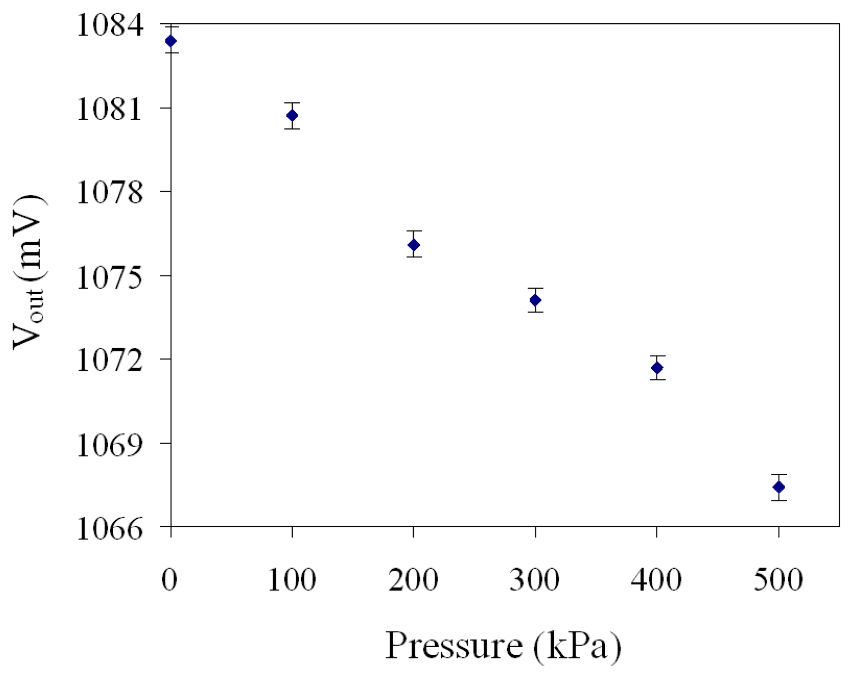
The FET pressure sensor integrated with the readout circuits, in which the circuits were applied to convert the output current of the pressure sensor into the output voltage. The power supply provided the Vds voltage of 3.3 V and the Vgs voltage of 3 V to the FET pressure sensor, and the output voltage of the FET pressure sensor with the readout circuits was measured at different pressures using an oscilloscope. Figure 16 shows the relation between the pressure and output voltage for the pressure sensor. The measured results revealed that the output voltage of the pressure sensor varied from 1083.6 to 1067.6 mV as the pressure changed from zero to 500 kPa, and the curve was a linear with a slope of 0.032. Thereby, the pressure sensor had a sensitivity of 0.032 mV/kPa at Vds=3.3 V and Vgs=5 V under the pressure of 500 kPa.
Svensson et al. [9] and Hynes et al. [10] employed surface micromachining process to fabricate the FET pressure sensors without readout circuits. Comparing with Svensson et al. [9] and Hynes et al. [10], this work used the CMOS-MEMS process to manufacture the FET pressure sensor integrated with readout circuits on a chip, in which the output current of the FET pressure sensor was converted into the output voltage by the readout circuits. On the other hand, the pressure sensor reported by Lin et al. [5] had a sensitivity of 0.15mV/psi. Wu et al. [6] presented the pressure sensor that had a sensitivity of 177.6 μV/psi. A comparison with Lin et al. [5] and Wu et al. [6], the sensitivity of the pressure sensor in this work exceeded that of Lin et al. [5] and Wu et al. [6]. The capacitive pressure sensor proposed by Dai et al. [7] had a chip area of 2×2 mm2. The area of the FET pressure sensor in this work, which was about 0.6×0.8 mm2, was less than Dai et al. [7].
5. Conclusion
The FET pressure sensor integrated with readout circuits has successfully been implemented using the commercial CMOS process and a post-process. The FET pressure sensor generated a change in current upon applying pressure to the sensing cells, and the output current of the pressure sensor was converted into the output voltage by the readout circuits. The FET pressure sensor needed a post-process to release the suspended membranes after completion of the CMOS process. In the post-process, the etchants were used to etch the sacrificial layers to release the membranes of the pressure sensor, and then the LPCVD parylene was utilized to seal the etch holes in the pressure sensor. The pressure sensor consisted of 16 sensing cells in parallel, which could increase the output current. The CoventorWare was utilized to simulate the stress and displacement of the pressure sensor. The simulated results revealed that the displacement at the center of the membrane was about 0.44 μm at the pressure of 500 kPa. The characteristics of the circuits were evaluated using the HSPICE, and the results depicted that the operational amplifier had a dc open loop gain of 93. Finally, the experiments showed that the pressure sensor had a sensitivity of 0.032 mV/kPa at Vds=3.3 V and Vgs=3 V in the 0-500 kPa pressure range.
Acknowledgments
The authors would like to thank National Center for High-performance Computing (NCHC) for chip simulation, National Chip Implementation Center (CIC) for chip fabrication and the National Science Council of the Republic of China for financially supporting this research under Contract No NSC 96-2221-E-005-081.
Reference
- Eggers, T.; Marschner, C.; Marschner, U.; Clasbrummel, B.; Laur, R.; Binder, J. Advanced hybrid integtaed low-power telemetric pressure monitoring system for biomedical application. Proc. IEEE Micro Electro Mech. Syst. 2000, 329–334. [Google Scholar]
- Huang, J.T.; Cheng, S.C. Study of injection molding pressure sensor with low cost and small probe. Sens. Actuators A 2002, 101, 269–274. [Google Scholar]
- Berns, A.; Buder, U.; Obermeier, E.; Wolter, A. AeroMEMS sensor array for high-solution wall press measurments. Sens. Actuators A 2006, 132, 104–111. [Google Scholar]
- Pulliam, W.; Russler, P.; Mlcak, R.; Murphy, K.; Kozikowski, C. Micromachined, SiC fiber optic pressure sensors for high-temperature aerospace applications. Proc. SPIE 2000, 4202, 21–30. [Google Scholar]
- Lin, L.; Yun, W. Design, optimization and fabrication of surface micromachined pressure sensors. Mechatronics 1998, 8, 505–519. [Google Scholar]
- Wu, C.H.; Zorman, C.A.; Mehregany, M. Fabrication and testing of bulk micromachined silicon carbide piezoresistive pressure sensors for high temperature applications. IEEE Sensors J. 2006, 6, 316–323. [Google Scholar]
- Dai, C.L.; Chang, S.C.; Lee, C.Y.; Cheng, Y.C.; Chang, C.L.; Chiou, J.H.; Chang, P.Z. Capactive micro pressure sensors with underneath readout circuit using a stand CMOS process. J. Chin. Inst. Eng. 2003, 26, 237–241. [Google Scholar]
- Sippola, C.B.; Ahn, C.H. A thick film screen-printed ceramic capacitive pressure microsensor for high temperature applications. J. Micromech. Microeng. 2006, 16, 1086–1091. [Google Scholar]
- Svensson, L.; Plaza, J.A.; Benitez, M.A.; Esteve, J.; Lora-Tamayo, E. Surface micromachining technology applied to the fabrication of a FET pressure sensor. J. Micromech. Microeng. 1996, 6, 80–85. [Google Scholar]
- Hynes, E.; O'Neill, M.; McAuliffe, D.; Berney, H.; Lane, W.A.; Kelly, G.; Hill, M. Development and characterization of a surface micromachined FET pressure sensor on a CMOS process. Sens. Actuators A 1999, 76, 283–292. [Google Scholar]
- Kim, J.W.; Takao, H.; Sawada, K.; Ishida, M. Integrated inductors for RF transmitters in CMOS/MEMS smart microsensor systems. Sensors 2007, 7, 1387–1398. [Google Scholar]
- Cheng, Y.C.; Dai, C. L.; Lee, C.Y.; Chen, P.H.; Chang, P.Z. A circular micromirror array fabricated by a maskless post-CMOS process. Microsys. Technol. 2005, 11, 444–451. [Google Scholar]
- Dai, C.L.; Chen, Y.L. Modeling and manufacturing of micromechanical RF switch with inductors. Sensors 2007, 7, 2660–2670. [Google Scholar]
- Senturia, S.M. Microsystem Design; Kluwer Academic: Boston, 2001; p. p. 196. [Google Scholar]
- Reismann, H.; Pawlik, P.S. Elasticity theory and applications; JohnWiley & Sons: New York, 1980. [Google Scholar]
Figure 1.
Layout of the FET pressure sensor with circuits.
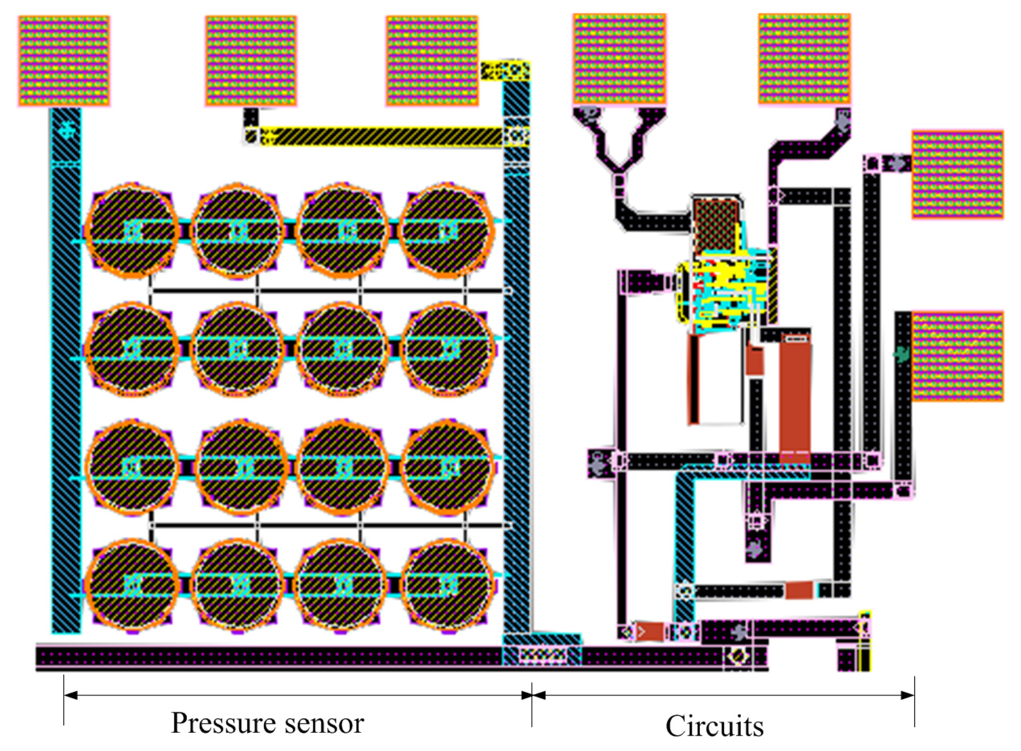
Figure 2.
Schematic cross-sectional view of a sensing cell.

Figure 3.
Stress distribution of the membrane.

Figure 4.
Displacement of the membrane.

Figure 5.
Relation between pressure and displacement at the center of the membrane.
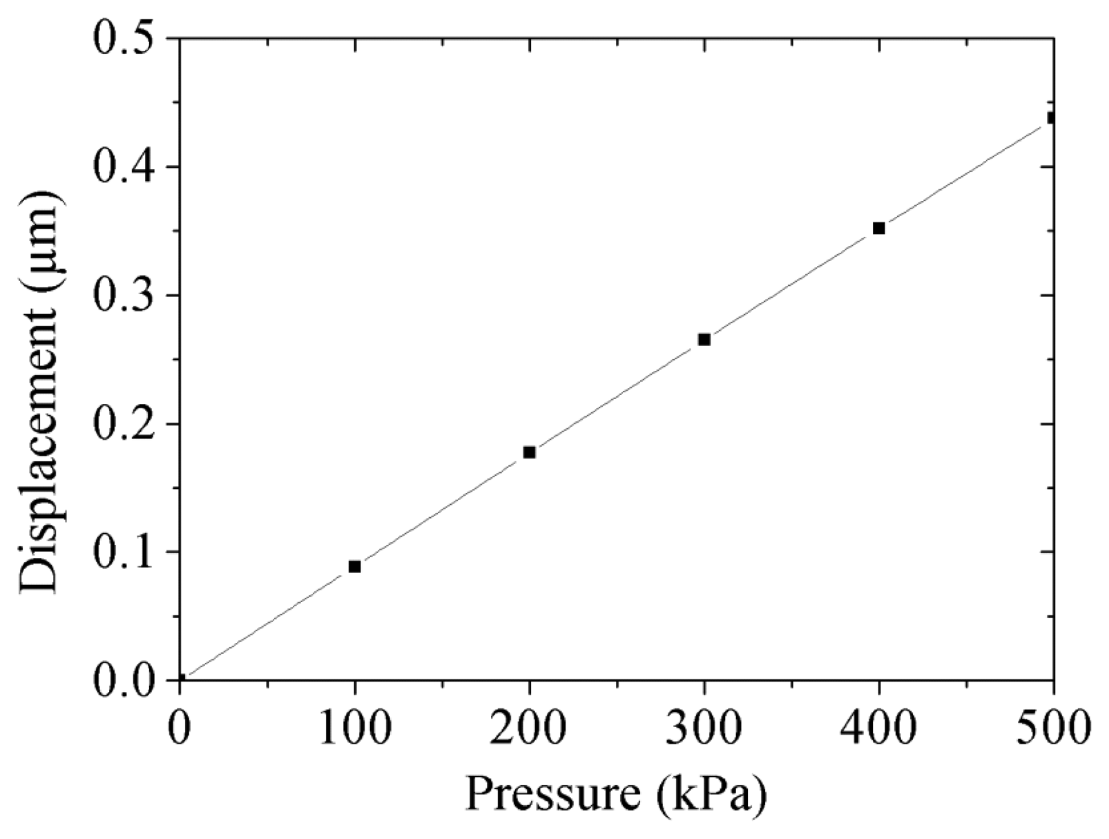
Figure 6.
Simulation of Ids/ Vds characteristics for the FET pressure sensor.
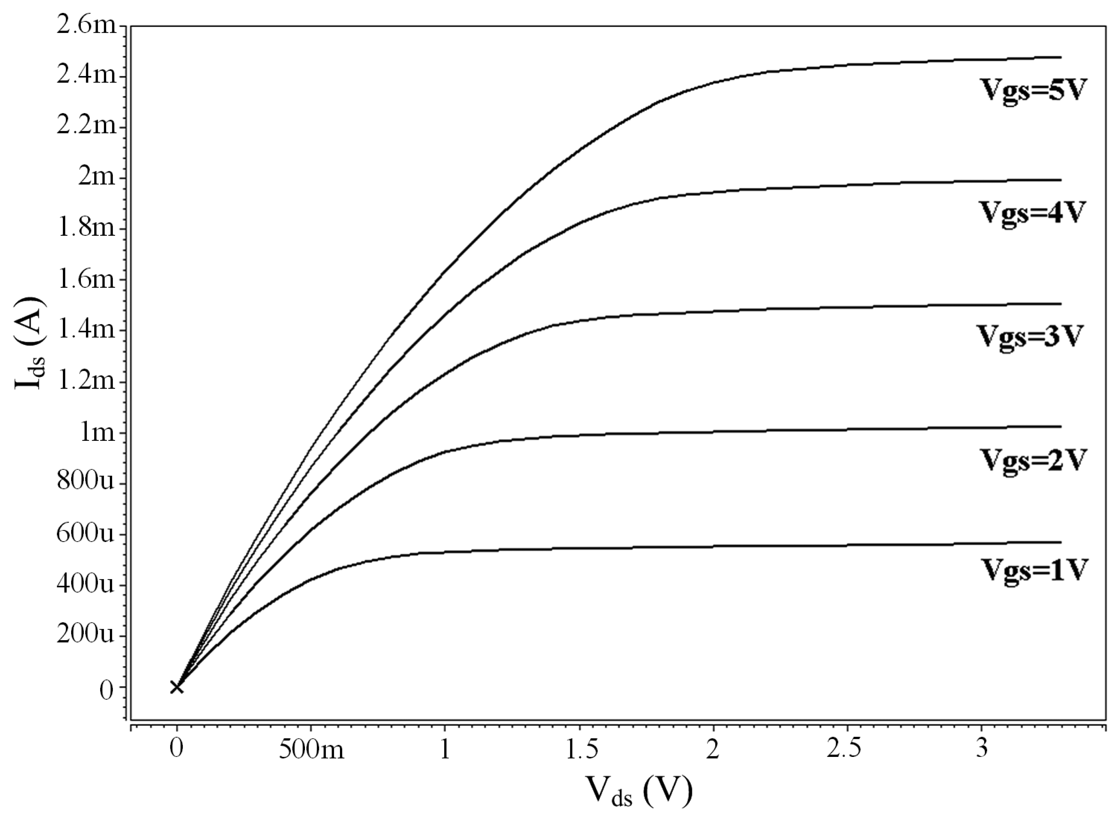
Figure 7.
Readout circuits.
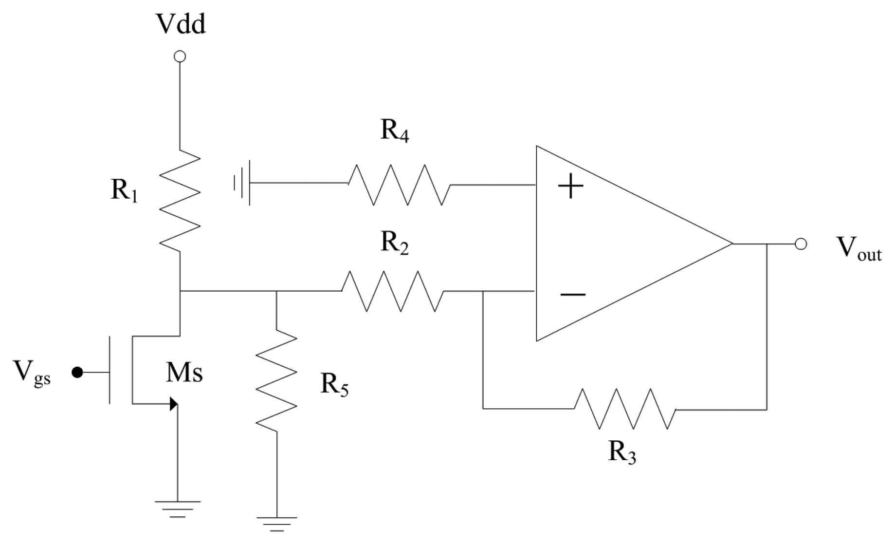
Figure 8.
Design of the operational amplifier circuit.
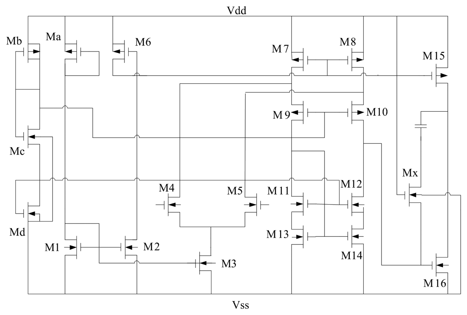
Figure 9.
Frequency response of the operational amplifier.
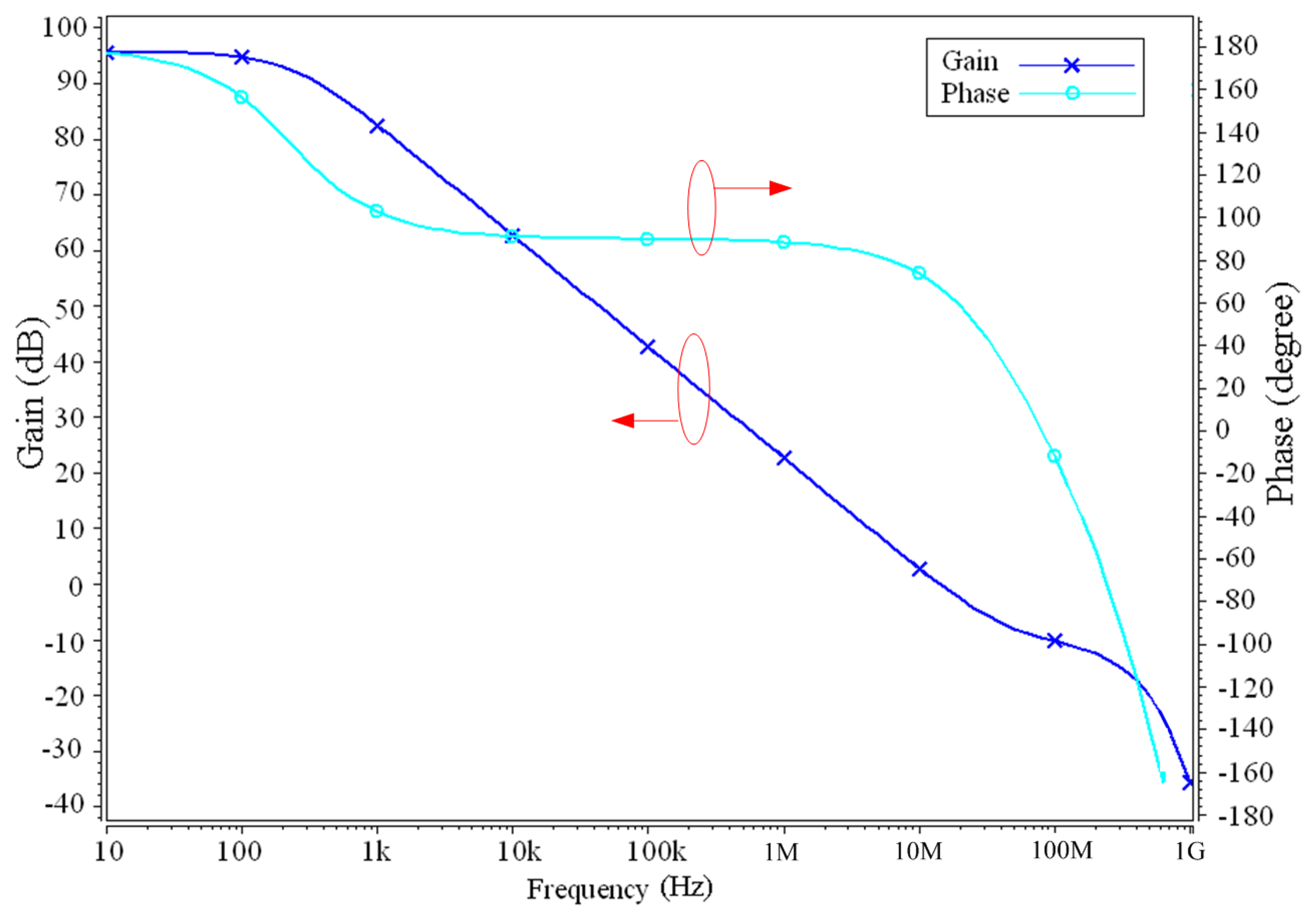
Figure 10.
Simulated results of the readout circuits
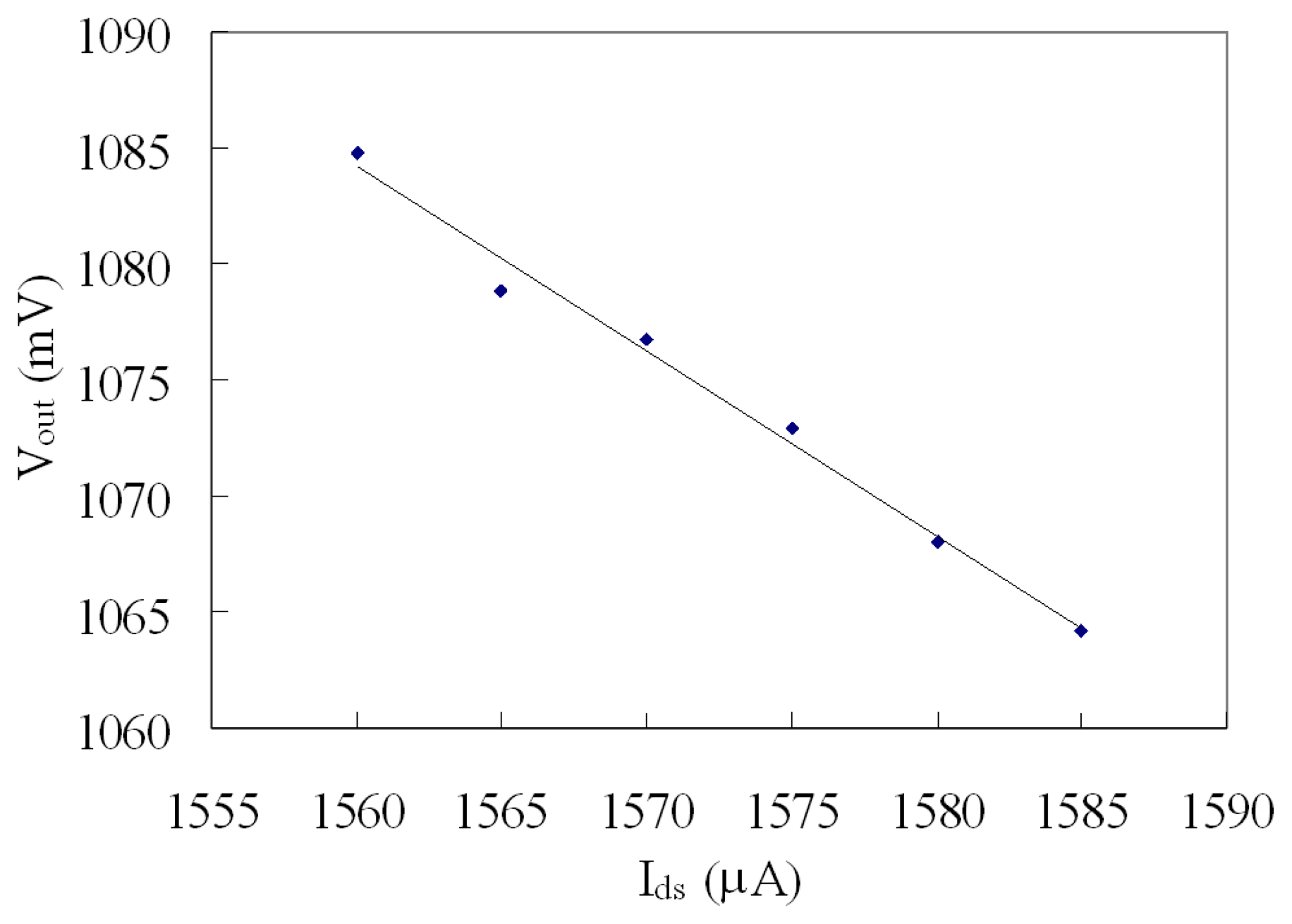
Figure 11.
Process flow of the FET pressure sensor: (a) after completion of CMOS process, (b) etching the sacrificial layers, and (c) sealing the etch holes.
Figure 11.
Process flow of the FET pressure sensor: (a) after completion of CMOS process, (b) etching the sacrificial layers, and (c) sealing the etch holes.
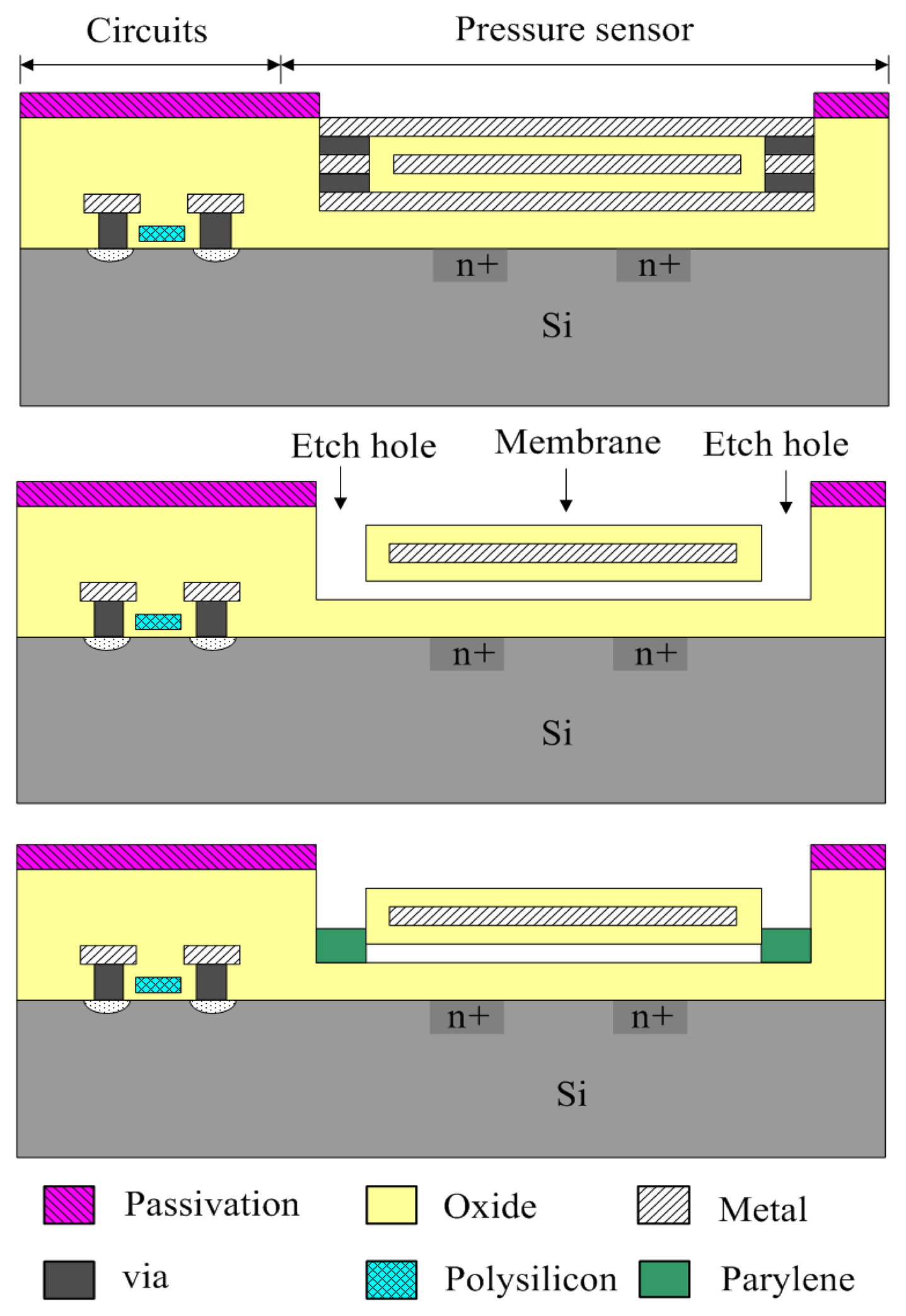
Figure 12.
Photograph of the FET pressure sensor with circuits after the wet etching process.
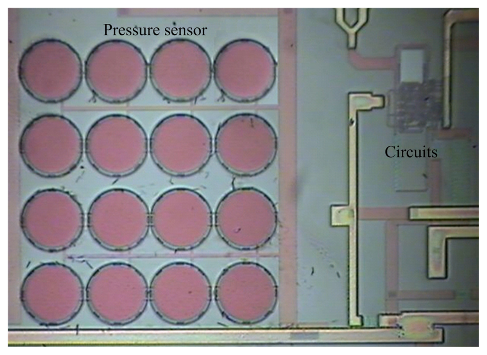
Figure 13.
SEM image of the FET pressure sensor after the wet etching process.

Figure 14.
Measurement of Ids/Vds characteristics for the FET pressure sensor.
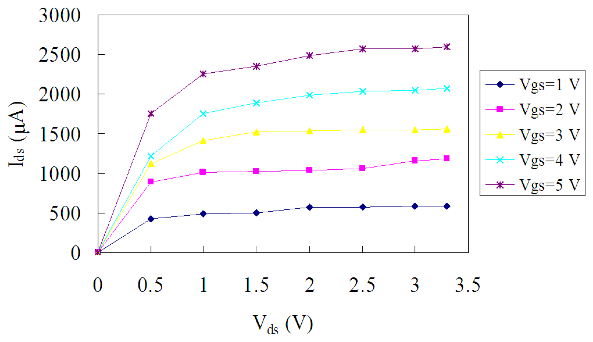
Figure 15.
Output current of the FET pressure sensor without circuits.

Figure 16.
Output voltage of the FET pressure sensor with circuits.
© 2007 by MDPI ( http://www.mdpi.org). Reproduction is permitted for noncommercial purposes.
Share and Cite
MDPI and ACS Style
Dai, C.-L.; Tai, Y.-W.; Kao, P.-H. Modeling and Fabrication of Micro FET Pressure Sensor with Circuits. Sensors 2007, 7, 3386-3398. https://doi.org/10.3390/s7123386
AMA Style
Dai C-L, Tai Y-W, Kao P-H. Modeling and Fabrication of Micro FET Pressure Sensor with Circuits. Sensors. 2007; 7(12):3386-3398. https://doi.org/10.3390/s7123386
Chicago/Turabian StyleDai, Ching-Liang, Yao-Wei Tai, and Pin-Hsu Kao. 2007. "Modeling and Fabrication of Micro FET Pressure Sensor with Circuits" Sensors 7, no. 12: 3386-3398. https://doi.org/10.3390/s7123386