Reliability of a MEMS Actuator Improved by Spring Corner Designs and Reshaped Driving Waveforms

Institute of Photonics and Optoelectronics, National Taiwan University, 1, Roosevelt Road, Section 4, Taipei, Taiwan
*
Author to whom correspondence should be addressed.
Sensors 2007, 7(9), 1720-1730; https://doi.org/10.3390/s7091720
Submission received: 19 July 2007
/
Accepted: 31 August 2007
/
Published: 3 September 2007
(This article belongs to the Special Issue Modeling, Testing and Reliability Issues in MEMS Engineering)
Abstract
:In this paper, we report spring corner designs and driving waveforms to improve the reliability for a MEMS (Micro-Electro-Mechanical System) actuator. In order to prevent the stiction problems, no stopper or damping absorber is adopted. Therefore, an actuator could travel long distance by electromagnetic force without any object in moving path to absorb excess momentum. Due to long displacement and large mass, springs of MEMS actuators tend to crack from weak points with high stress concentration and this situation degrades reliability performance. Stress distribution over different spring designs were simulated and a serpentine spring with circular and wide corner design was chosen due to its low stress concentration. This design has smaller stress concentration versus displacement. Furthermore, the resonant frequencies are removed from the driving waveform based on the analysis of discrete Fourier transfer function. The reshaped waveform not only shortens actuator switching time, but also ensures that the spring is in a small displacement region without overshooting so that the maximum stress is kept below 200 MPa. The experimental results show that the MEMS device designed by theses principles can survive 500 g (gravity acceleration) shock test and pass 150 million switching cycles without failure.
1. Introduction
During past few years, MEMS technology has enabled many types of sensors, actuators and systems to be reduced in size by orders of magnitude, while often even improving its performance, such as accelerometers, optical switches, biochemical analysis systems [1]. Especially in optical fiber communication, MEMS has attracted more and more attention because of the rapid growth of communication bandwidth. For high bit-rate and large bandwidth communication, data switching and routing between the nodes of network are critical issues. Conventional optical-electronic-optical (O-E-O) type switching has some disadvantages such as high maintain cost and latency resulting from header information processing [2]. Therefore, all optical (O-O-O) switching systems are proposed in the backbone of the communication system. MEMS technology shows great potentials for O-O-O system because of advantages on small size, batch process, and low costs. The function of signal switching on most MEMS devices is implemented by a micromirror which has a reflecting metal coating. A micromirror is actuated by an actuator to manipulate the light signal. The types of driving force include thermal, electro-static, and electromagnetic, etc [3]. In this paper, we considered electromagnetic force as the actuated force due to its low driving voltage and long traveling distance. Thus, electromagnetic actuators can move micromirrors several hundreds of micrometers with less than one-volt applied.
Reliability issue is important in optical communication. For a silicon-based MEMS device, the mechanical properties are relatively good. But springs made of silicon still need to be carefully designed to prevent fracture. It must be reliable especially in some critical environments, such as devices in a deep ocean. If a device is broken, rebuild or repair is quite expensive. In order to prevent the stiction problem, we removed stoppers which are usually seen in MEMS devices with large displacement [4]. Unfortunately, for a mechanical structure, springs may wear out after many operating cycles. The rate of worn out increases as the springs suffer more stress or large displacement.
To prevent spring failure or the reliability degradation, two improvements were discussed in this paper. First, the stress on different spring geometry designs was simulated by finite element method (FEM) to search out a proper design. Then, we developed a generic driving waveform to prevent overshoot phenomenon. By the aid of proper spring design and edited driving waveform, springs are limited to operate in a low stress region. Finally, the experimental results of the device that passed rigorous requirement are shown.
2. Stress Analysis of Spring Designs
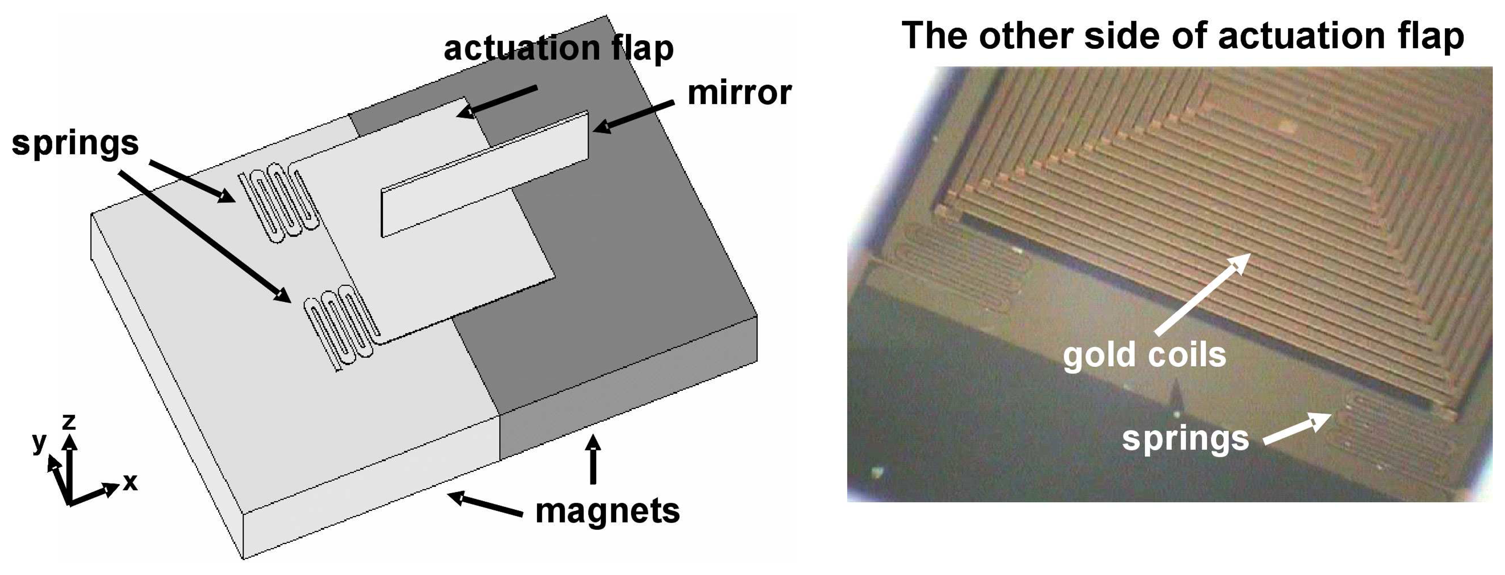
The MEMS actuator in this paper is actuated by electromagnetic force. The schematic drawing of a MEMS actuator is shown in Fig. 1. A flap is connected to substrate by two springs. The metal coils are patterned in back of a flap. Two permanent magnets with opposite polarity in z direction are placed underneath the flap. The magnetic flux comes from the north-pole and enters the south-pole. Because the flap is placed between boundaries of two magnets and is close to the magnet surface, the magnetic flux passing through the metal coil is quasi-uniform in x direction. When current flows through metal coils, an upward magnetic dipole, m, and magnetic flux in x direction, B, form a torque (m cross B). Thus, a flap is moved up and a vertical micromirror is out of cavity to reflect optical signal.
When the applied voltage is off, a flap is moved back to the initial position by springs. For a large electromagnetic force, a flap tends to vibrate before it stops. We have no stopper or damping absorber in moving path to reduce the vibration because the surface contact between flap and stopper has stiction issue and this degrades reliability. But springs are likely to fail for a long time operation or large vibration without proper designs.
Therefore, we simulated the stress distribution over different spring geometrical designs in order to find a proper solution. The simulation is done by ANSYS™, commercial software based on finite element method (FEM). Table 1 shows the parameters in simulations. For a silicon-based structure, Young's modulus is 165 GPa. Poisson ratio is 0.22 [5]. Density is 2330 Kg/m3. The width for the spring beam is 30 μm, and the thickness for flap and spring is 10 μm. The vertical micromirror is 500 μm high, 1200 μm long and 20 μm thick. The zero displacement setting was referred to the boundary condition clamped at the end of the serpentine spring. For an optical switch operation, a flap edge lifts up at 200 μm heights from initial position to ensure the entire Gaussian beam can be reflected without truncation. First, we compared stress distribution of springs with different length at 200 μm height deformation. Stress distribution on a long beam results in small stress intensity, but the trade off is space consumption. We took serpentine spring to save space. Fig. 2 (a) shows the simulation results for length effect. The length of long string is about 3000 μm, which is about three times longer than short one. The stress on long string is smaller than short one. The maximum stress intensity is 607 MPa and 210 MPa for a short and long string beam, respectively. This is mainly due to the longer beam length, the smaller deformation per unit length. However, both maximum stresses happen at sharp inner corner of serpentine springs and these results in weak points. The spring may break up easily at corners. In order to prevent high concentrated stress intensity at corners, the spring corner must be re-designed carefully. The stress can be further reduced by smoothing the inner corner and extending the corner width [6]. We used circular shape and 50 μm width corner instead of square one. The maximum stress intensity is reduced to 451 MPa and 136 MPa for a short and long string as shown in Fig. 2 (b). About 77% of the stress is reduced from short beam with square corner design (607 MPa) to long serpentine beam with circular corner design (136 MPa).
However, displacement of an actuator might be more than 200 μm under conditions of high input voltage, large vibration, and high gravity impact. At 200 μm displacement of an actuator, springs endure about 100 g acceleration due to gravity. Therefore, based on the final long beam and circular corner design, we make more comprehensive simulations for the stress versus different spring deformation. The displacement or height of flap is set from 200 μm to 1000 μm, which corresponds to 500 g. The results are summarized in Fig. 3. The long and circular corner spring design reduces the maximum stress effectively not only at small displacement but also at large deformation. Because the maximum stress intensity increases with displacement dramatically, this design has more benefits especially at large displacement region. The maximum stress intensity is 4109 MPa without any improvement of spring design, compared with 600 MPa with optimized design. Stress on a square spring is about seven times larger than that of a long and circular spring design. By proper spring corner design, MEMS devices are more likely to pass vibration and high gravity acceleration shock tests.
3. Reshaped Waveform for Actuating
According to the simulation results at the last section, an actuator must operate in a confined displacement region with low stress for high reliability requirement. However, a square voltage waveform caused it to vibrate dramatically. To overcome this problem, we developed a reshaped waveform instead of a square waveform.
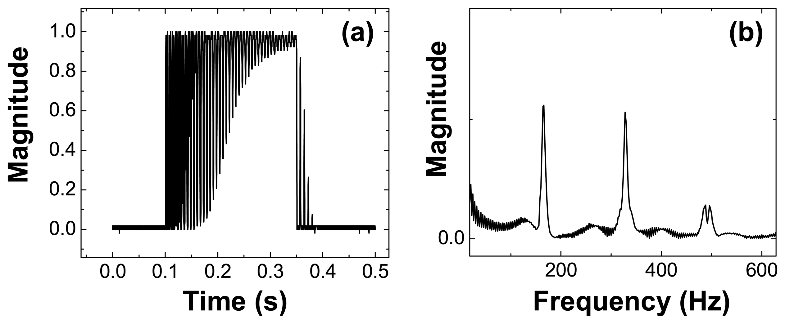
The concept of reshaped waveform editing is removing resonant components from a square waveform to reduce the vibrating amplitude on MEMS actuators. In order to record and analyze the vibration behavior, we setup two fiber ports which are perpendicular to the vibration direction. In our case, the flap becomes stable because of the energy consumption of air resistance or heat. This is similar to a simple harmonic oscillation with a damper. When the flap is up, the laser light from one port is reflected by a vertical micromirror to the other port. Thus, an optical intensity period refers to a vibration period. Then, the optical signals refer to a square driving waveform is recorded by an oscilloscope after an O/E conversion by an optical power meter, as in Fig. 4 (a). The actuator is an under-damping system so that the vibration last for about 350 ms.
The dominated factor of vibration is the resonant frequencies which refer to several peaks as shown in fig 4 (b). The peaks values are around 165 Hz, 330 Hz, and 490 Hz.
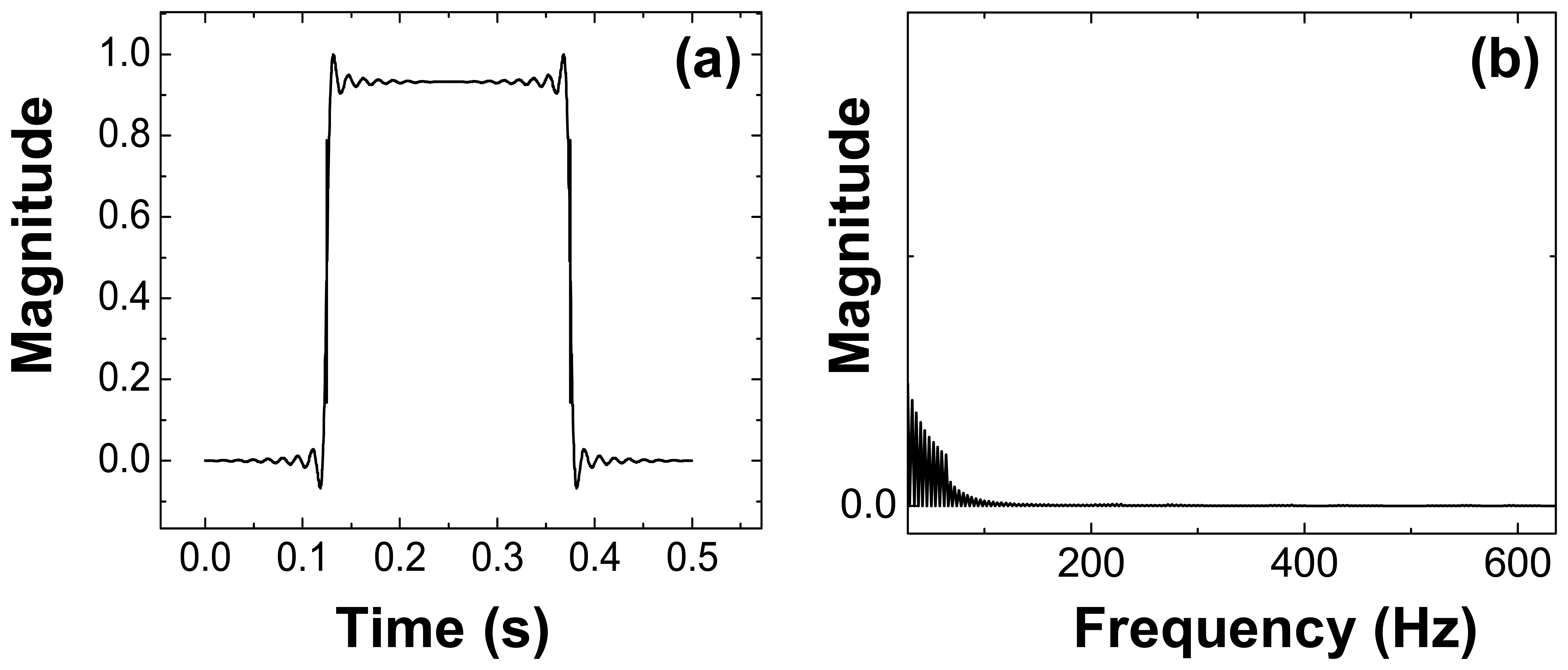
It can be confirmed experimentally. Fig. 5 shows the displacement of a flap when it is operated at 0 Hz, 1 Hz, 165 Hz, and 190 Hz. It is clear that the amplitude of vibration at 190 Hz (far from resonant peaks) is smaller than that at 165 Hz (near to a resonant peak). This is because the square waveform consists of a broadband spectrum and some frequencies cause large vibration or resonance. Therefore, the discrete square waveform signal is converted to frequency domain by discrete Fourier transform (DFT), as shown in Eq. 1, where xn represents N discrete voltage values and Xk represents N discrete values in frequency domain after DFT. Then, we reduced the magnitude around (about 100 frequency points) the resonant peaks by the factor with a reciprocal Gaussian distribution. Eq. 3 shows the Gaussian distribution, where A, B, C, and σ are adjustable parameters. A is the height of the Gaussian peak and C is the position of the center of the peak. When B is equal to 0.5, σ represents the standard deviation which determined the width of Gaussian distribution. We adjusted the value A as 14.8, B as 0.5, σ as 25. This can avoid magnitude jump, which leads to a ringing in edited driving waveform. Finally, an inverse discrete Fourier transform (IDFT), as shown in Eq. 2, is performed to obtain a new waveform in time domain. The new driving waveform without resonant components is called reshaped driving waveform.
Briefly, we drove a MEMS device with square waveform and recorded the output optical signal in time domain which contains vibration information. Then, a reshaped waveform was edited by the analysis of vibration information in the frequency domain. The DFT calculation based on fast Fourier transform (FFT) algorithms is implemented [7] by Matlab™, a suite of commercial software for mathematical calculation. The final reshaped waveform is shown in Fig. 6 and its experimental results will be discussed in the next section.
4. Experimental Results and Discussion
To fabricate optical MEMS switches with smooth and vertical reflecting surfaces, we started with double-sided polished SOI wafers with the (110) substrate and the (100) device layer, which were fusion bonded together. LTO silicon dioxide was first deposited and patterned as the wet etching masks. Using anisotropic TMAH wet etching, vertical walls are created on the (111) planes of the substrate wafer and used as the reflecting mirror. The height of the fabricated micromirror is about 500 μm, the thickness is approximately 20 μm and the length is around 1200 μm. After vertical mirrors were created, the first gold layer was deposited by E-beam evaporator on the membrane. Then, the low temperature PECVD (plasma enhanced chemical vapor deposition) silicon nitride was applied as an insulation layer, which was followed by the second gold layer deposition. We used wet gold etchant to pattern coils on the front side of the SOI wafer for generating electromagnetic force along with external magnetic fields provided by permanent magnets, as shown in Fig. 1. Then the flap and serpentine springs were patterned by deep reactive ion etching (DRIE) on the device layer to release the micro-actuators [8]. The turning corners of serpentine springs were made with the same shape as shown in Fig. 2. The inner corners of the serpentine springs were rounded to minimize stress concentration. The width of the turning corner is increased to further reduce the stress concentration. The width of the corners is about twice of that of straight torsion bar.
With the newly designed serpentine springs, the newly fabricated devices went through rigorous reliability tests including shock, vibration and mechanical cycling, as described in the GR-1221 from Telcordia Technologies [9]. We performed the reliability tests on bare chips first to visually check whether the redesigned serpentine springs can meet the test requirements without any visible cracks under a high-resolution microscope. After that, chips selected randomly from other fabrication batches were packaged with fiber collimators to verify the new spring design by optical insertion loss. The optical insertion loss of each package was measured before and after the tests with the same individual driving current. The passing criterion is that the insertion loss difference, measured before and after the test, should be less than ±0.5 dB according to GR-1221. Should any tiny crack occur on the springs, the insertion loss difference would be large after applying the same driving current because optical alignment has drifted away from the original optimized position.
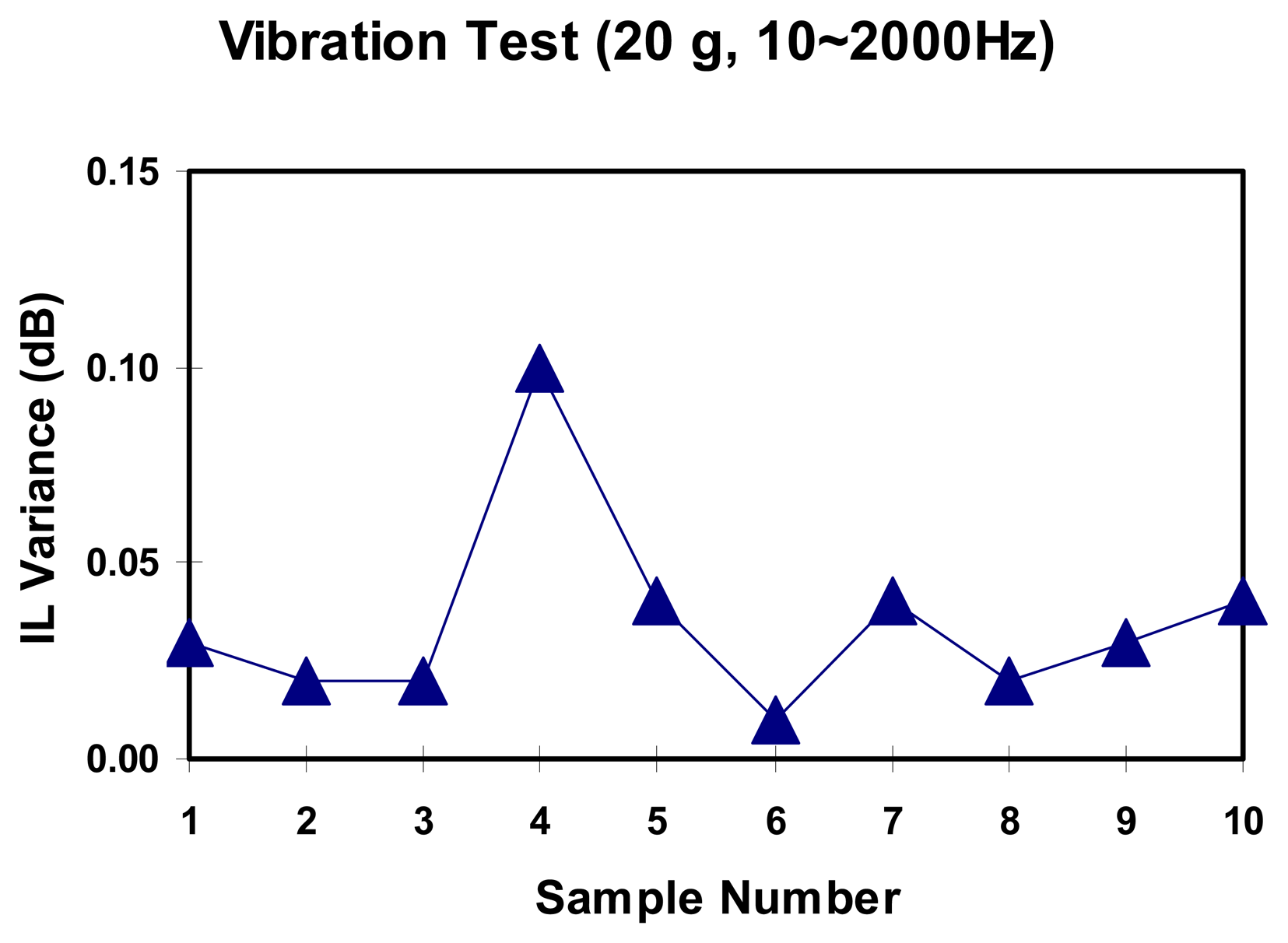
The vibration test was done by mounting samples on a vibration machine with an in-situ accelerometer in close loop control. The amplitude of the vibration was 20 g with the sweeping frequency from 10 Hz to 2000 Hz and back to 10 Hz in 20 minutes. The test was performed 12 cycles per axis, in three mutual perpendicular axes. The final result is shown in Fig. 7 with all ten pieces passing the test.
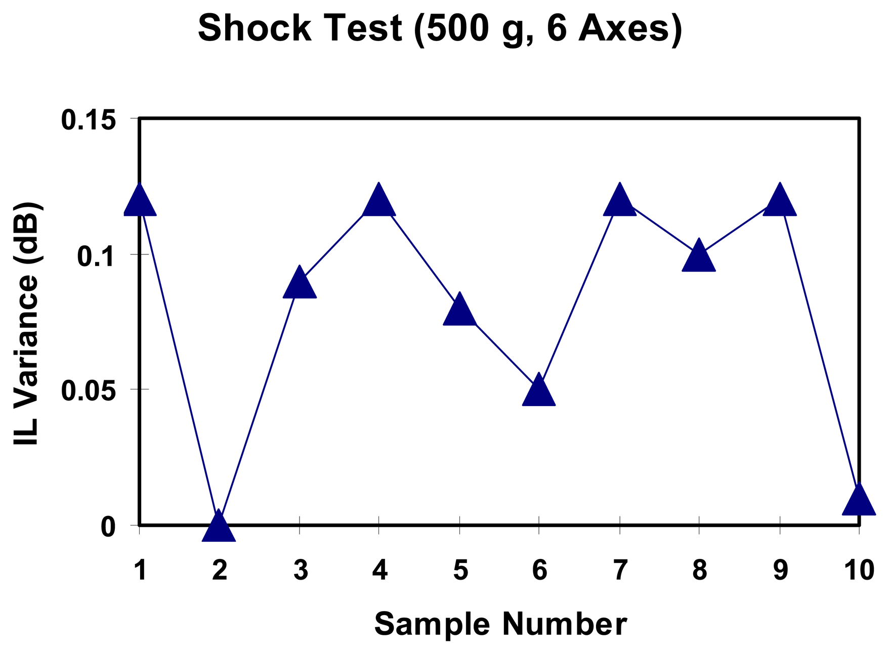
In the mechanical shock, the test was performed in three mutually perpendicular axes, two directions in each axis and five times per direction. There were a total of 30 shocks for each optical switch. The amplitude of mechanical shock (impact) is 500 g with one milli-second duration. In order to attain meaningful statistic data, there were ten samples subjected to the shock test to evaluate the redesigned serpentine springs. The results are shown in Fig. 8. The Y-axis shows the insertion loss difference and the X-axis represents the pieces of samples. The maximum delta insertion loss is within 0.15 dB and there are no samples that had failed after the shock test. This proves the newly designed spring corners passed the shock test. Before the redesign of serpentine springs, the most often seen failure modes of shock/vibration tests of square spring design were the broken micro-spring at the turning corners around 500 g shock, as the prediction in the FEM simulations shown in the previous section. After redesigning the corner shape of the serpentine springs, we find that the broken parts are moved from corners to straight part of the springs. The serpentine springs fail at approximately a 1200 g mechanical shock.
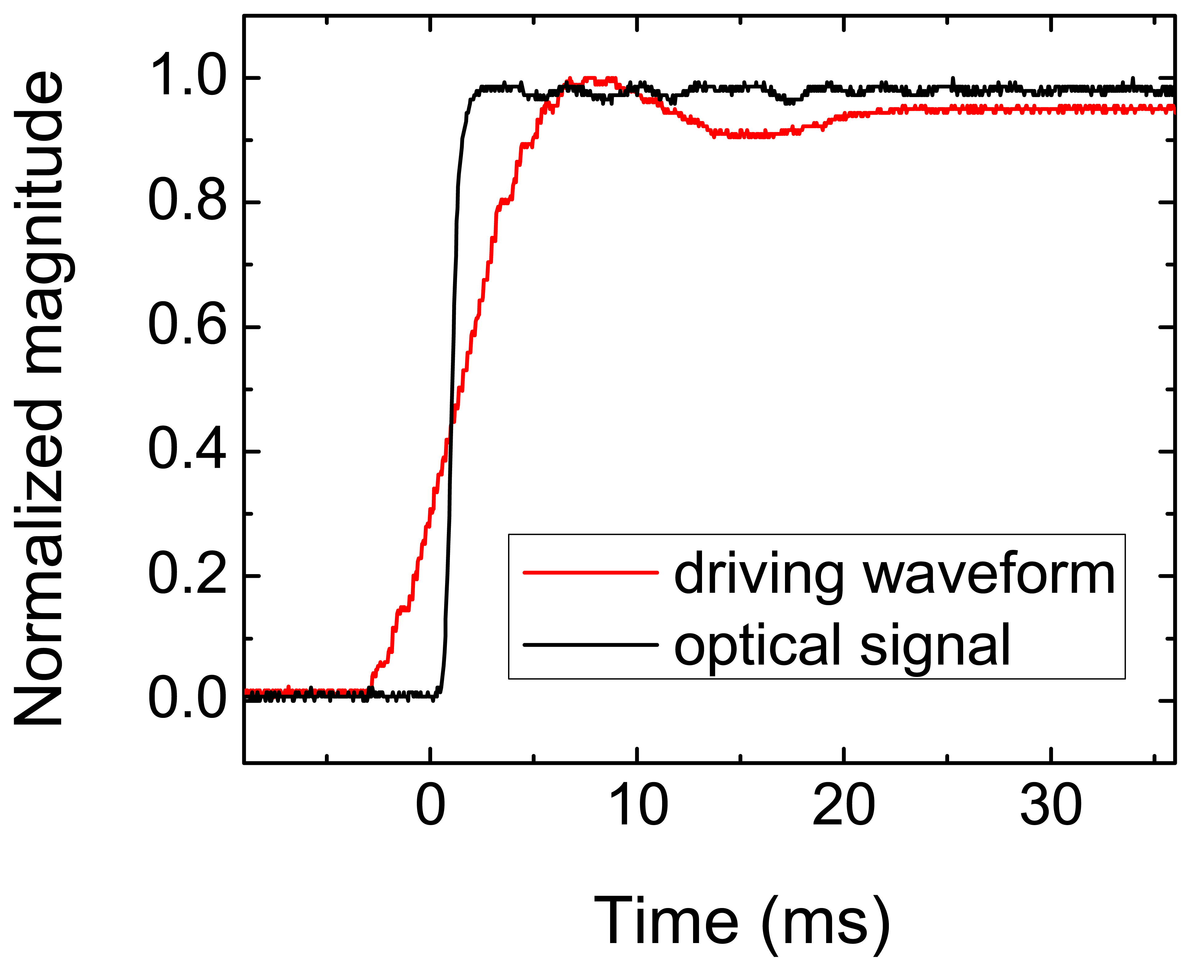
Finally, we performed a long-term cycling test on packaged switches. With reshaped driving waveform, we can minimize the overshoot of MEMS actuators so that the stress on the springs can be minimized. We have operated ten switches over 150 million cycles and all ten switches passed without any failure, as shown in Fig. 9. The insertion loss variance was less than 0.15 dB, which suggest that there was no crack on springs. Another side advantage of the edited waveform is that the switching time can be improved to 10 ms, as shown in Fig. 10. The switching is measured based on Telcordia standard. It is measures from the initial application of driving waveform to the time which takes the optical signal to 90% of the steady state optical power level. Compared with Fig. 4 (a), the switching time is reduced from 350 ms to 10 ms by removing the resonant frequency components.
5. Conclusion
A highly reliable MEMS device is achieved by the proper design of the spring beam structure and reshaped driving waveform. According to the FEM simulation results by ANSYS, the wider corner and long spring beam design spreads the stress distribution and prevents stress from localization which results in spring failure. The reshaped driving waveform based on Fourier transfer function is implemented by mathematical calculation. It reduces the resonant amplitude effectively and the spring deformation is limited in preferred region. Reshaped driving waveform also improves switching time to 10 ms. Both spring designs and driving waveforms assure that actuators operate in the low stress region with high reliability. The experimental results confirmed above design principles. The devices successfully passed 20 g vibration, 500 g shock and 150 million cycling test.
References
- Kovacs, G. T. Micromachined Transducers Sourcebook; McGraw-Hill, 1998. [Google Scholar]
- Morris Iii, A. S. In search of transparent networks. IEEE Spectrum 2001, 38, 47–51. [Google Scholar]
- Ma, X. H.; Kuo, G. S. Optical switching technology comparison: Optical mems vs. other technologies. IEEE Communications Magazine, 2003 Nov; pp. S16–S23.
- Horsley, D. A.; Davis, W. O.; Hogan, K. J.; Hart, M. R.; Ying, E. C.; Chaparala, M.; Behin, B.; Daneman, M. J.; Kiang, M. Optical and mechanical performance of a novel magnetically actuated MEMS-based optical switch. Journal of Microelectromechanical Systems 2005, 14, 274–284. [Google Scholar]
- Dolbow, J.; Gosz, M. Effect of out-of-plane properties of a polyimide film on the stress fields in microelectronic structures. Mechanics of Materials 1996, 23, 311–321. [Google Scholar]
- Su, G. J.; Hung, S.; Jia, D.; Jiang, F. Serpentine spring corner designs for micro-electro-mechanical systems optical switches with large mirror mass. Optical Review 2005, 12, 339–344. [Google Scholar]
- Hsieh, H.; Su, G. J. Compact 1x2 MEMS optical switches with low-actuation voltage. Proceedings of SPIE 2006, v 6038, 60381W–9. [Google Scholar]
- Su, G. J.; Chiu, E.; Jiang, F. Vertical Micromirrors Integrated with Electromagnetic Microactuators for 2-Dimesional Optical Matrix Switches. IEEE Photonics Technology Letters 2005, vol. 17(no. 9), 1860–1862. [Google Scholar]
- Generic Reliability Assurance Requirements for Passive Optical Components; Telcordia Standards GR-1221, 1999.
Figure 1.
Schematic drawing of a MEMS optical switch.

Figure 2.
Stress analysis (a) beam length effect, and (b) corner design effect.
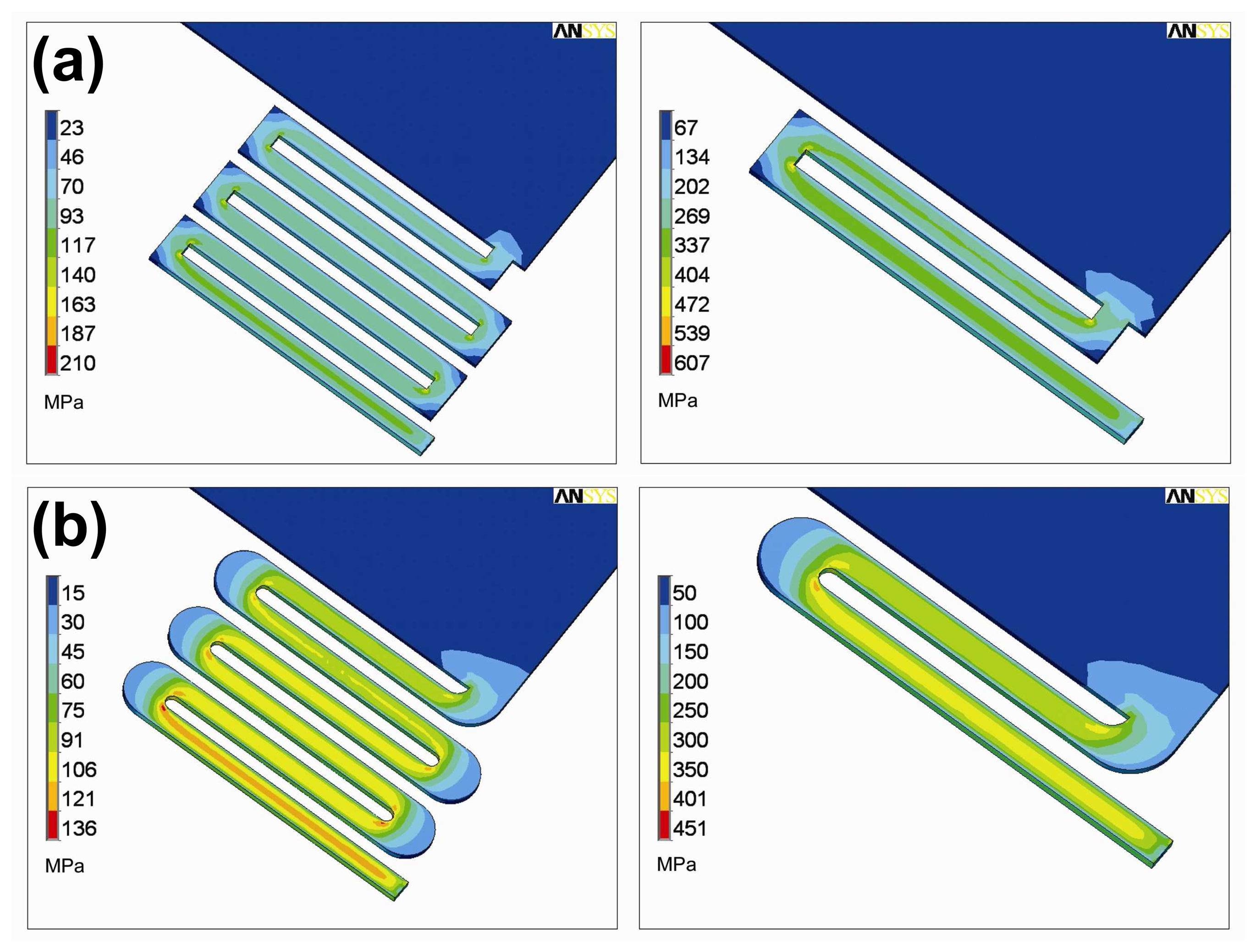
Figure 3.
Displacement vs. stress over different spring designs.
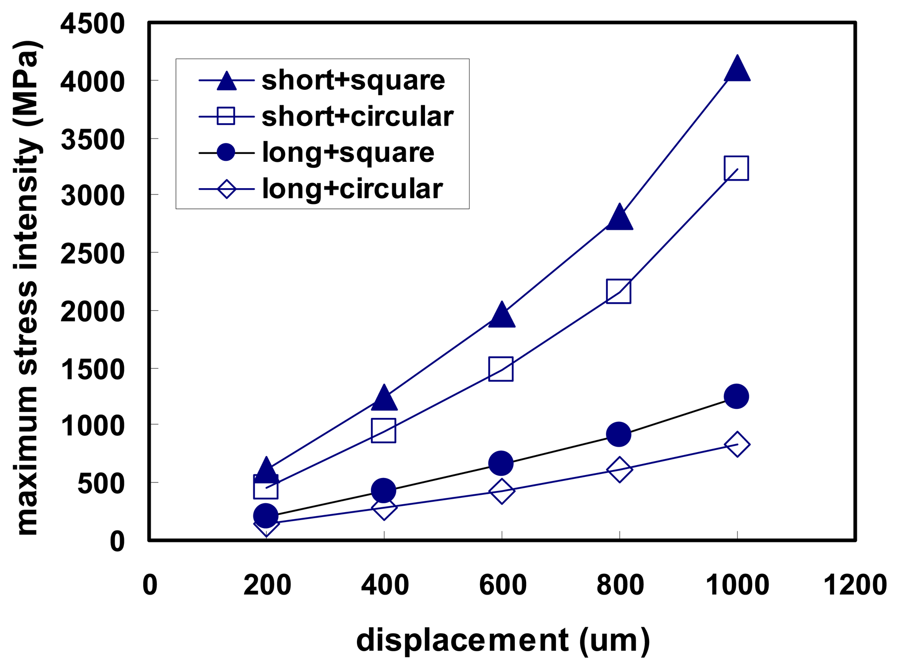
Figure 4.
MEMS device actuated by square waveform (a) switching time and (b) its frequency analysis.
Figure 4.
MEMS device actuated by square waveform (a) switching time and (b) its frequency analysis.

Figure 5.
Pictures of MEMS devices operated at frequency of (a) 0 Hz (b) 1 Hz (c) 165 Hz (d) 190 Hz.
Figure 5.
Pictures of MEMS devices operated at frequency of (a) 0 Hz (b) 1 Hz (c) 165 Hz (d) 190 Hz.
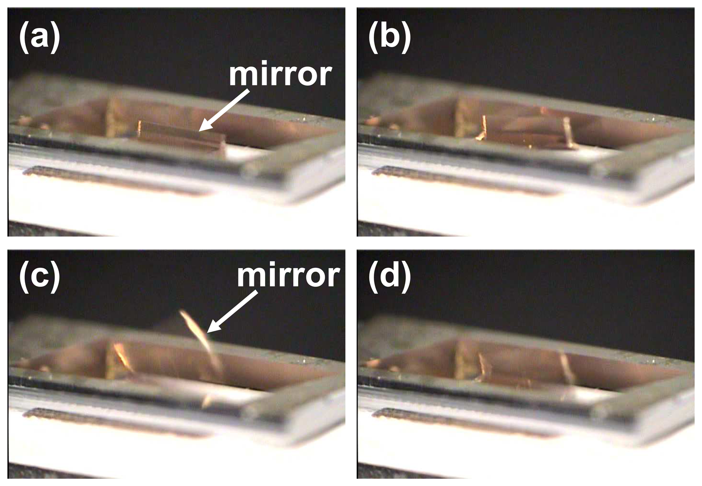
Figure 6.
Reshaped waveform in (a) time domain, and (b) in frequency domain.

Figure 7.
Vibration test over 10 pieces.

Figure 8.
Shock test over 10 pieces.

Figure 9.
150 million cycles over 10 pieces.
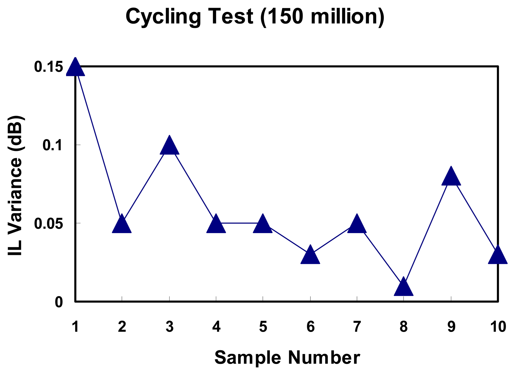
Figure 10.
Switching time achieved by edited waveform.

| Parameters | Values | Units |
|---|---|---|
| Young's modulus | 165 | GPa |
| Poisson ratio | 0.22 | |
| Density | 2330 | Kg/m3 |
© 2007 by MDPI ( http://www.mdpi.org) Reproduction is permitted for noncommercial purposes.
Share and Cite
MDPI and ACS Style
Hsieh, H.-T.; Su, G.-D.J. Reliability of a MEMS Actuator Improved by Spring Corner Designs and Reshaped Driving Waveforms. Sensors 2007, 7, 1720-1730. https://doi.org/10.3390/s7091720
AMA Style
Hsieh H-T, Su G-DJ. Reliability of a MEMS Actuator Improved by Spring Corner Designs and Reshaped Driving Waveforms. Sensors. 2007; 7(9):1720-1730. https://doi.org/10.3390/s7091720
Chicago/Turabian StyleHsieh, Hsin-Ta, and Guo-Dung John Su. 2007. "Reliability of a MEMS Actuator Improved by Spring Corner Designs and Reshaped Driving Waveforms" Sensors 7, no. 9: 1720-1730. https://doi.org/10.3390/s7091720