A Review of the CMOS Buried Double Junction (BDJ) Photodetector and its Applications

Abstract
:
1. Introduction
2. The BDJ Photodetector Device
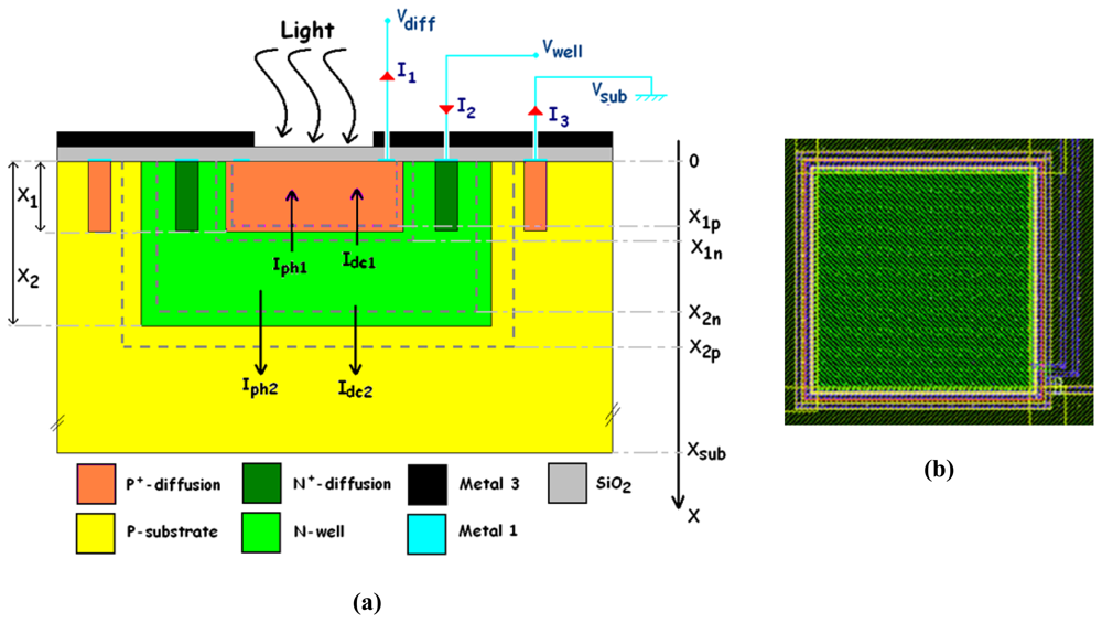
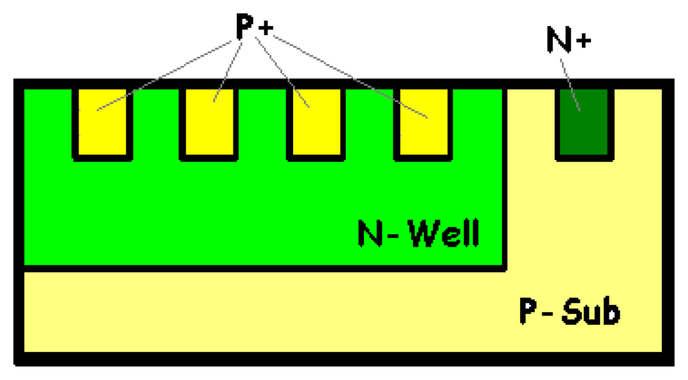
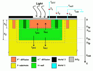
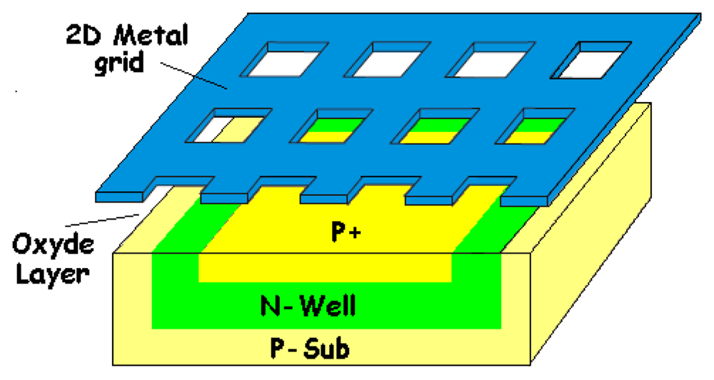
2.1. Structure and operation
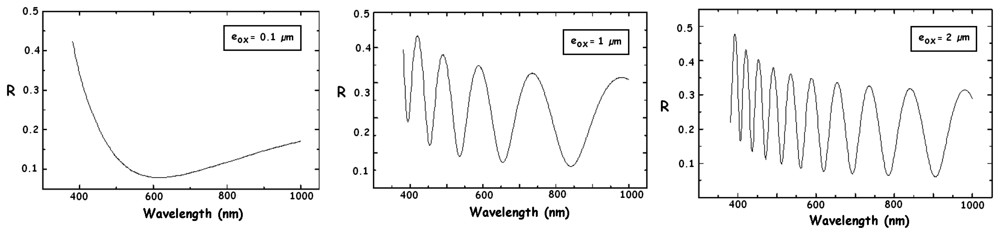
2.2. Surface reflection
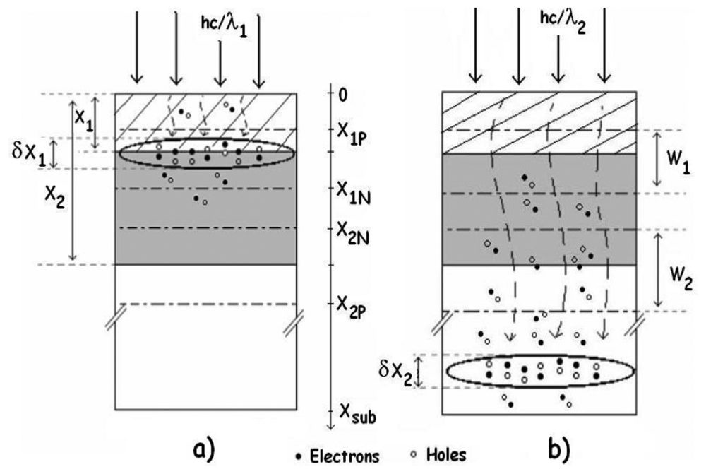
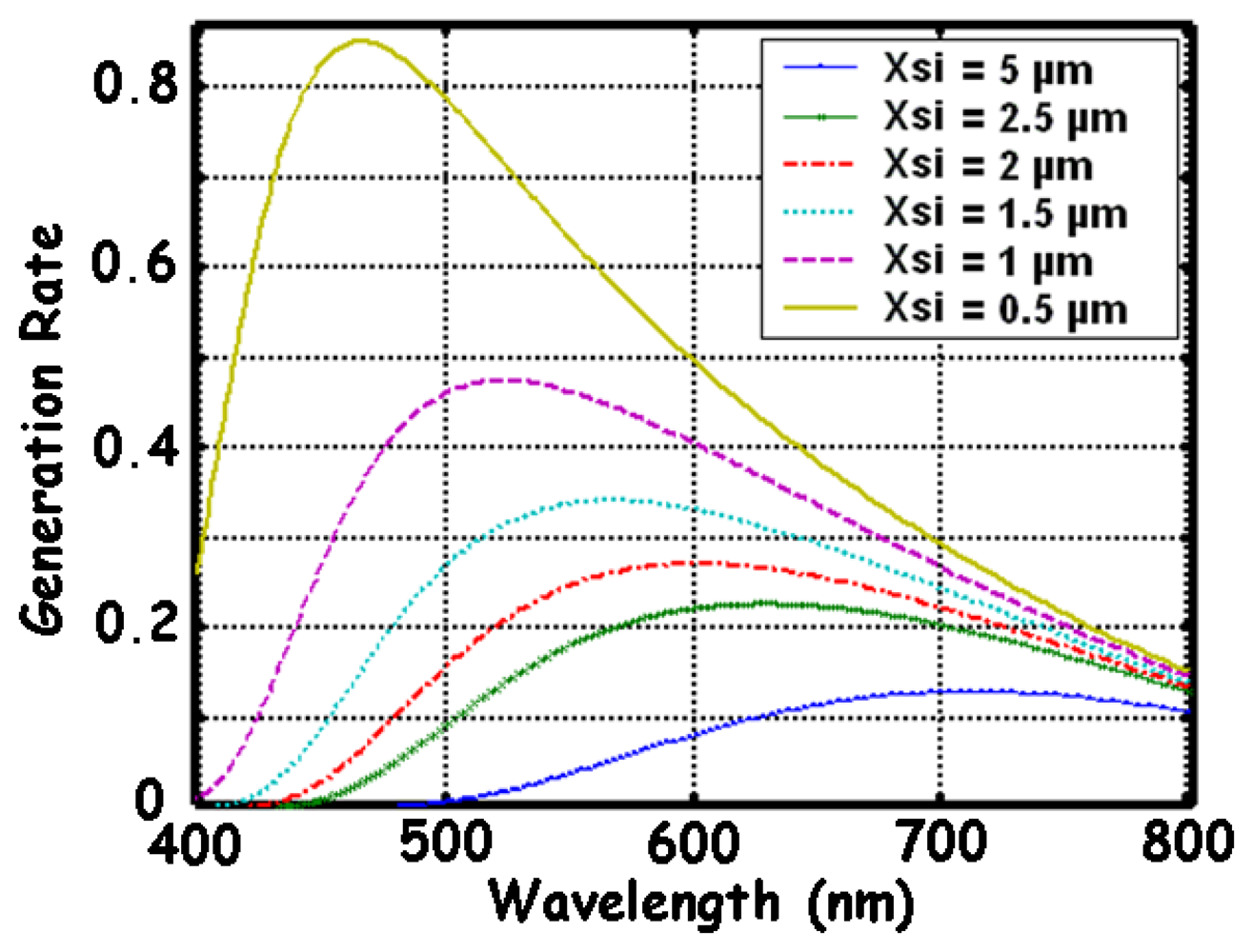
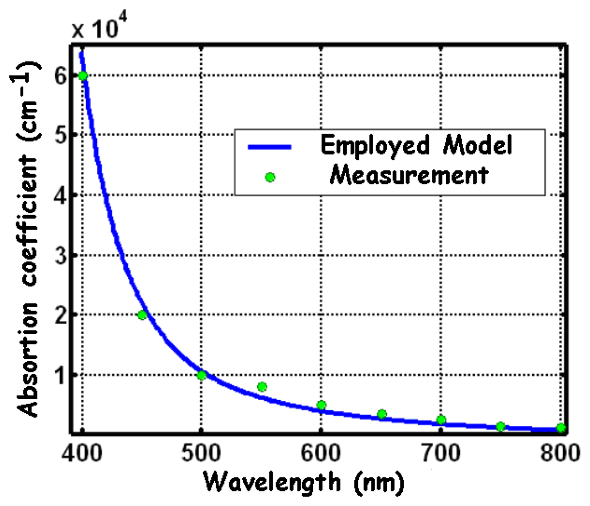
2.3. Light absorption in silicon and generation rate of electron-hole pairs
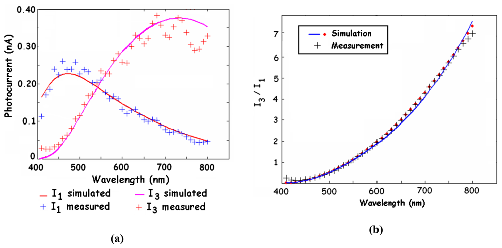
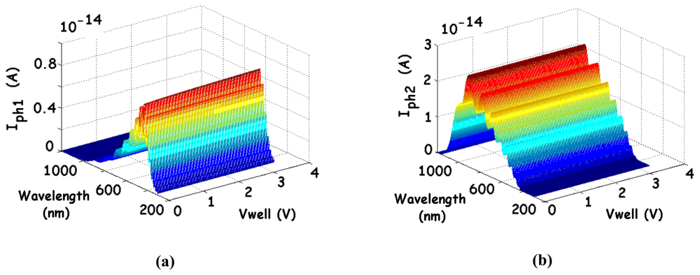
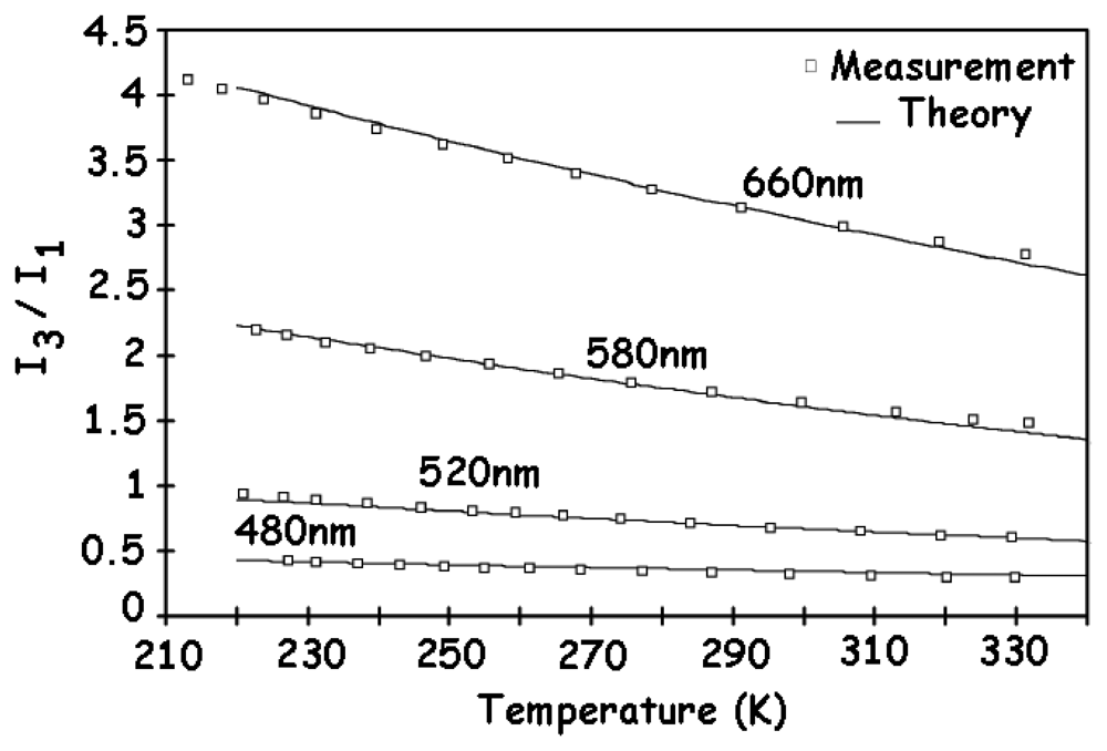
2.4. Photocurrents
2.5. Response time
- ▪
- which yields τdiff comprised between 0.13 ns and 0.15 ns, with a CMOS 0.8μm technology;
- ▪
- τNwell is in the range [0.14 ns; 0.16 ns];
- ▪
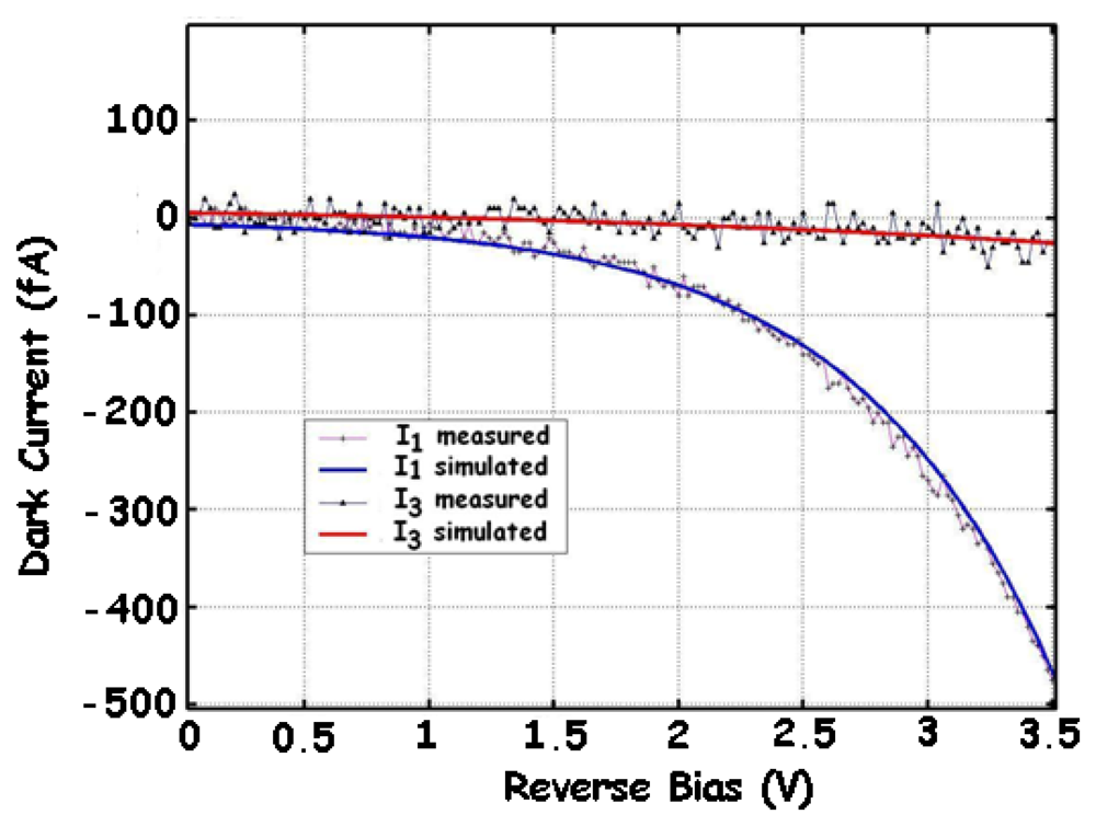
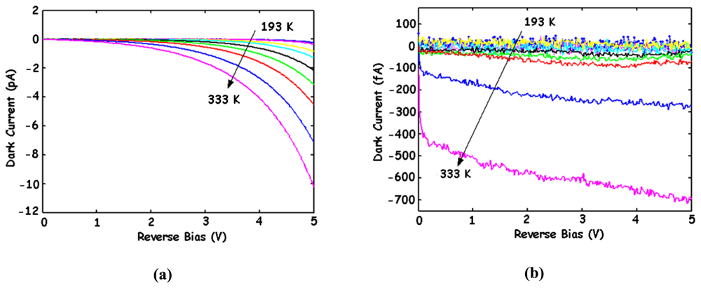
2.6. Dark currents
3. BDJ SPICE model
3.1. Large-signal, small-signal and noise models
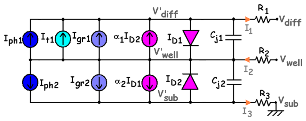
3.1.1. Large-signal model
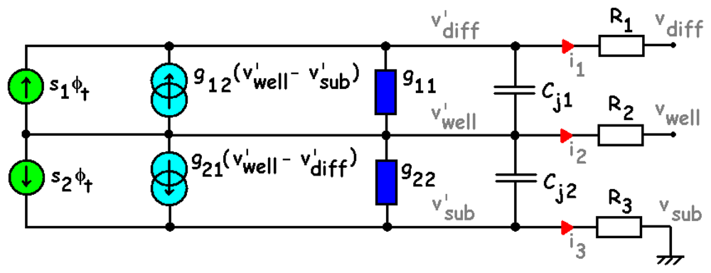
3.1.2. Small-signal model
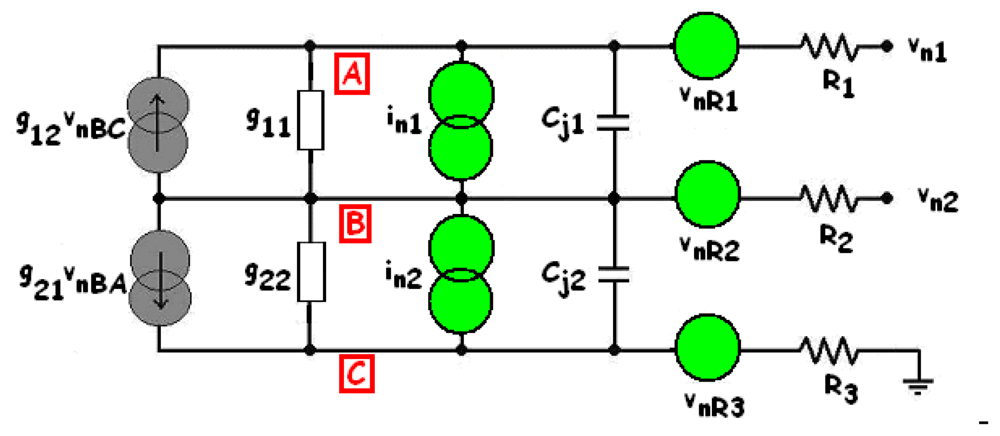
3.1.3. Noise model
3.2. Models implementation in CAD tools
4. Design and process considerations
4.1. Solutions to reduce dark currents
4.2. Solutions to improve quantum efficiency and Signal-to-Noise Ratio
5. Examples of applications in integrated CMOS optical sensors
6. Conclusions
References and Notes
- Fossum, E.R. Active Pixel Sensor: Are CCDs Dinosaurs? In Proc. SPIE; San Jose, CA, USA, February 6-10 1994; Volume 2172, pp. 2–14. [Google Scholar]
- Meynants, G.; Dierickx, B.; Scheffer, D. CMOS Active Pixel Image Sensor with CCD Performance. In Proc. SPIE; San Diego, CA, USA, July 19 1998; Volume 3410, pp. 68–76. [Google Scholar]
- Sedjil, M. Modélisation de Capteurs de Couleur Intégré et Développement d'Application; Thesis, University D. Diderot, Paris, 1999.
- Ben Chouikha, M. Développement de Détecteurs de Couleur dans des Technologies Standards de CI (CMOS et BiCMOS): Application à la Réalisation de Capteurs Intégrés pour l'Imagerie Electronique et l'Instrumentation; Thesis, University D. Diderot, Paris, 1999.
- Ben Chouikha, M.; Lu, G.N.; Sedjil, M.; Sou, G. A Photodetector Based on Buried Junctions and Corresponding Method of Manufacture. US Patent. No 08/816383, 1996. [Google Scholar]
- Ben Chouikha, M.; Viénot, F. Colorimetric Characterisation of Color Detector, Implanted in a BiCMOS Technology. In Proc. IS&T/SPIE; San Jose, CA, January, 1999; Volume 9, pp. 105–110. [Google Scholar]
- Sedjil, M.; Lu, G.N.; Ben Chouikha, M.; Alexandre, A. Modeling of BDJ and BTJ Structures for Color Detection. In Proc. SPIE; Denver, CO, USA, July 18 1999; Volume 3680, pp. 388–397. [Google Scholar]
- Lu, G.N.; Ben Chouikha, M.; Sou, G.; Sedjil, M. Color Detection Using a Buried Double p-n Junction Implanted in the CMOS Process. Electron. Lett. 1996, 35, 594–596. [Google Scholar]
- Lu, G.N.; Ben Chouikha, M.; Sedjil, M.; Sou, G.; Alquie, G. Investigation of the Buried Double p-n Junction Implanted in CMOS Technology for Wavelength-Sensitive Detection. Int. J. Electron. 1997, 83, 307–316. [Google Scholar]
- Alexandre, A.; Ben Chouikha, M.; Sedjil, M.; Alquie, G. An improved BDJ Photodetector Physical Model under Spice. In Proc. MSM; San Diego, CA, 2000; Ch. 5; pp. 189–192. [Google Scholar]
- Alexandre, A.; Lu, G.N.; Chea, A.; Sedjil, M.; Ben Chouikha, M. Modèles Spice de Deux Nouveaux Capteurs Optiques Intégrés (BDJ et BTJ) pour le Développement de Microsystèmes. In C2I, Instrumentation, Interdisciplinarité et Innovation.; Colloque interdisciplinaire en instrumentation: Paris, France, November 1998; pp. 403–410. [Google Scholar]
- Alexandre, A.; Sou, G.; Ben Chouikha, M.; Sedjil, M.; Lu, G.N.; Alquie, G. Modeling and Design of Multi Buried Junctions Detectors for Color Systems Development. In Proc. SPIE; San Diego, CA, USA, July 30 2000; Volume 4019, pp. 288–298. [Google Scholar]
- Lu, G.N.; Sou, G.; Devigny, F.; Guillaud, G. Design and Testing of a CMOS BDJ Detector for Integrated Micro-Analysis. Microelectronics 2001, 32, 227–234. [Google Scholar]
- Ben Chouikha, M.; Lu, G.N.; Sedjil, M.; Sou, G. A CMOS Linear Array of BDJ Color Detector. In Proc. SPIE; San Diego, CA, USA, July 19 1998; Volume 3410, pp. 46–53. [Google Scholar]
- Wolffenbuttel, R.F. Silicon Photodetectors with a Selective Spectral Response. In Sensors Update; Baltes, H., Hesse, J., Korvink, J., Eds.; Wiley: New York, 2001; Volume 9, pp. 69–101. [Google Scholar]
- Middelhoek, S.; Audet, S.A. Silicon Sensors; Academic Press: New York, 1989. [Google Scholar]
- Feruglio, S.; Haned, F.; Vasilescu, G.; Ben Chouikha, M.; Sou, G.; Fouad Hanna, V.; Alquie, G. A General Model of the CMOS Buried Double Junction Photodetector. In Proc. IEEE IST; Lyon, France, June 2004; pp. 60–65. [Google Scholar]
- Feruglio, S.; Vasilescu, G.; Alquie, G.; Fouad Hanna, V. Modelling of the CMOS Buried Double Junction Photodetector. Microw. Opt. Techn. Lett. 2005, 45, 507–514. [Google Scholar]
- Feruglio, S.; Fouad Hanna, V.; Alquie, G.; Vasilescu, G. Dark Current and Signal-to-Noise Ratio in BDJ Image Sensors. IEEE Trans. Instrum. Meas. 2006, 55, 1892–1903. [Google Scholar]
- Feruglio, S. Etude du Bruit dans les Capteurs d'Images Intégrés, type APS; Thesis, University Pierre & Marie Curie, Paris, 2005.
- Dillon, P.L.; Brault, A.T.; Horak, J.R.; Garcia, E.; Martin, T.W.; Light, W.A. Fabrication and Performance of Colour Filter Arrays for Solid-State Imagers. IEEE Trans. Electron. Dev. 1978, 25, 97–101. [Google Scholar]
- Mathieu, H. Physique des semi-conducteurs et des composants électroniques; Ed. Masson: Paris, 1998. [Google Scholar]
- Toffano, Z. Optoélectronique, Composants photoniques et fibres optiques; Ed. Ellipses; Paris, 2001. [Google Scholar]
- Lee, J.S.; Hornsey, R.I. Photoresponse of Photodiode Arrays for Solid-State Image Sensor. J. Vaccum. Sci. Technol. 2000, 18, 621–625. [Google Scholar]
- Lalanne, P.; Rodier, J.-C. CMOS Photodiode Based on Vertical p-n-p Junctions. Proc. WOCS. 1997. http://ipdps.cc.gatech.edu/1997/wocs/lalanne.pdf.
- Sze, S.M. Physics of Semiconductor Devices, 2ND ed.; J. Wiley & Sons: New York, 1981. [Google Scholar]
- Alexandre, A.; Ben Chouikha, M.; Alquie, G. Identification de l'épaisseur de l'oxyde de silicium et des longueurs de diffusion dans les différentes couches d'un capteur optique intégré silicium. In OHD Conf.; Besançon, France, September 1999. [Google Scholar]
- Huen, T. Reflectance of Thinly Oxidized Silicon at Normal Incidence. Appl. Optics 1979, 18, 1927–1931. [Google Scholar]
- Geist, J.; Migdall, A.; Baites, H.-P. Analytic Representation of the Silicon Absorption Coefficient in the Indirect Transition Region. Appl. Optics 1988, 27, 3777–3779. [Google Scholar]
- McLean, T.P. The Absorption Edge Spectrum of Semiconductors. Prog. Semiconductors 1960, 5, 53. [Google Scholar]
- Rajkanan, K.; Singh, R.; Shewchun, J. Absorption Coefficient of Silicon for Solar Cell Calculations. Solid-State Electron. 1979, 22, 793–795. [Google Scholar]
- Dash, W.C.; Newman, R. Intrinsic Optical Absorption in Single-Crystal Germanium and Silicon at 77K and 300K. Phys. Rev. 1955, 99, 1151–1155. [Google Scholar]
- Philipp, H.R.; Taft, E.A. Optical Constant of Silicon in the Region 1 to 10 eV. Phys. Rev. 1960, 120, 37–38. [Google Scholar]
- Kuhl, C.; Schlotterer, H.; Schwidefsky, F. Optical Investigation of Different Silicon Film. J. Electrochem. Soc.: Solid-State Sci. Tech. 1974, 121. No. 11. [Google Scholar]
- Varshni, Y.P. Temperature Dependence of the Energy Gap in Semiconductors. Physica 1967, 34, 149. [Google Scholar]
- Rajkanan, M.; Singh, R.; Schewchun, J. Absorption Coefficient of Silicon for Solar Cell Calculations. Solid-State Electron. 1979, 22, 793–795. [Google Scholar]
- Dash, W.C.; Newman, R. Intrinsic Optical Absorption in Single-Crystal Germanium and Silicon at 77°K and 300°K. Phys. Rev. 1955, 99, 1151–1155. [Google Scholar]
- Schmid, P.E. Optical Absorption in Heavily Doped Silicon. J. Am. Phys. Soc. 1981, 23, 5531–5536. [Google Scholar]
- Loukianova, N.V.; Folkerts, H.O.; Maas, J.P; Verbugt, D.W.E.; Mierop, A.J.; Hoekstra, W.; Roks, E.; Theuwissen, A.J.P. Leakage Current Modelling of Test Structure for Characterization of Dark Current in CMOS Image Sensor. IEEE Trans. Electron. Dev. 2003, 50, 77–83. [Google Scholar]
- Alexandre, A.; Pinna, A.; Granado, B.; Garda, P. Modeling and simulation of phototransistors using VHDL-AMS. In DCIS; Bordeaux, France, November 2004. [Google Scholar]
- Dadouche, F.; Alexandre, A.; Pinna, A.; Granado, B.; Garda, P. A VHDL-AMS Configuration for Active Pixel Sensors. In FDL Conf.; Lille, France, September 2004. [Google Scholar]
- Dadouche, F.; Pinna, A.; Garda, P.; Alexandre, A. Modeling of Pixel Sensors for Image Systems with VHDL-AMS. In Proc. IEEE DTIS; Tunisia, September 5-7 2006; pp. 289–293. [Google Scholar]
- Alexandre, A.; Dadouche, F.; Garda, P. Two Dimensional Model for Lateral Photodiode. In Proc. IEEE DTIS; Tunisia, September 5-7 2006; pp. 294–298. [Google Scholar]
- Dadouche, F.; Pinna, A.; Garda, P.; Alexandre, A. Modeling of Pixel Sensors for Image Systems with VHDL-AMS. Int. J. Electron. 2008, 95, 211–225. [Google Scholar]
- Ben Chouikha, M.; Vienot, F.; Lu, G.N. Temperature Effect on Colorimetric Accuracy of the BTJ Color Detector. In Proc. SPIE; Denver, CO, USA, July 18 1999; Volume 3410, pp. 204–214. [Google Scholar]
- Vasilescu, G. Electronic Noise and Interfering Signals: Principles and Applications; Springer-Verlag: Heidelberg, Germany, 2005. [Google Scholar]
- Vandamme, L.K.J. Noise as a Diagnostic Tool for Quality and Reliability of Electronic Devices. IEEE Trans. Electron. Dev. 1994, 41, 2176–2187. [Google Scholar]
- El Gamal, A.; Fowler, B.; Min, H.; Liu, X. Modeling and Estimation of FPN Components in CMOS Image Sensors. In Proc. SPIE; San Diego, CA, USA, July 19 1998; Volume 3301, pp. 168–177. [Google Scholar]
- Johansson, R. Implementation of an Active Pixel Sensor with Shutter and Analog Summing in a 0.35 μm Process. Thesis, University of Linköping, 2003.
- Haned, F.; Ben Chouikha, M.; Alquie, G. An Improved BDJ Color Detector Physical Model. In MOS Modeling and Parameter Extraction Workshop; Strasbourg, France, April 2005. [Google Scholar]
- Haned, F.; Ben Chouikha, M.; Alquie, G. Temperature Effect on the Buried Double Junction Color Detector Behavior. In Proc. IEEE MIXDES Conf.; Gdynia, Poland, June 2006; pp. 107–110. [Google Scholar]
- Haned, F.; Ben Chouikha, M.; Alquie, G. I-V Characterization for a Deeper Comprehension of Buried Double Junction Color Detector Behavior. In ICNMT Conf.; Tizi-Ouzou, Algeria, November 2006. [Google Scholar]
- Feruglio, S.; Garda, P.; Vasilescu, G. Noise Characterization of a CMOS Two-colour APS. MOC Tech. Dig. 2005, 114–115. [Google Scholar]
- Feruglio, S.; Fouad Hanna, V.; Alquie, G.; Vasilescu, G. Temporal Signal-to-Noise Ratio of a CMOS Buried Double Junction Image Sensor. In Proc. SPIE; San Jose, CA, USA, February 27 2005; Volume 5846, pp. 180–191. [Google Scholar]
- Feruglio, S.; Fouad Hanna, V.; Alquie, G.; Vasilescu, G. Exact Noise Analysis of a CMOS BDJ APS. In Proc. IEEE ISCAS; Kobe, Japan, May 2005; Volume 3, pp. 2337–2340. [Google Scholar]
- Feruglio, S.; Pinna, A.; Chay, C.; Llopis, O.; Granado, B.; Alexandre, A.; Garda, P.; Vasilescu, G. Noise Characterization of CMOS Image Sensors. In Proc. WSEAS CSCC; Athens, Greece, 2006; pp. 102–107. [Google Scholar]
- Laker, K.R.; Sansen, W.M.C. Design of Analog Integrated Circuits and Systems; McGraw-Hill: New York, 1994. [Google Scholar]
- Aharoni, H.; Ohmi, T. Analysis of n+p Silicon Junctions with Varying Substrate Doping Concentrations Made Under Ultra Clean Processing Technology. J. Appl. Phys. 1997, 81, 1270–1288. [Google Scholar]
- Kleinpenning, T.G.M. 1/f Noise in p-n Junction Diodes. J. Vacuum Sci. Technol. A 1985, 3, 176–182. [Google Scholar]
- Feruglio, S.; Pinna, A.; Llopis, O.; Chay, C.; Granado, B.; Alexandre, A.; Garda, P.; Vasilescu, G. Noise Characterization in a CMOS 0.6-μm PPS Image Sensors System. WSEAS Trans. Circ. Syst. 2006, 5, 877–886. [Google Scholar]
- Ravezzi, L.; Dalla Betta, G.-F.; Stoppa, D.; Simon, A. A Versatile Photodiode SPICE Model for Optical Microsystem Simulation. Microelectr. J. 2000, 31, 277–282. [Google Scholar]
- Alexandre, A.; Sou, G.; Ben Chouikha, M.; Sedjil, M.; Lu, G.N.; Alquie, G. Modeling and Design of Multi Buried Junctions Detectors for Color Systems Development. In Proc. SPIE; San Diego, CA, USA, July 30 2000; Volume 4019, pp. 288–298. [Google Scholar]
- Alexandre, A.; Sedjil, M.; Ben Chouikha, M.; Alquie, G. Modeling and Simulation Under SPICE of Optoelectronic Systems Including BDJ Detector. In Proc. SPIE; San Diego, CA, USA, July 29 2001; Volume 4408, pp. 138–146. [Google Scholar]
- Neifeld, M.A.; Chou, W.-C. SPICE-Based Optoelectronic System Simulation. Appl. Optics 1998, 37, 6093–6104. [Google Scholar]
- Desai, N.R.; Hoang, K.V.; Sonek, G.J. Applications of PSPICE Simulation Software to the Study of Optoelectronic Integrated Circuits and Devices. IEEE Trans. Edu. 1993, 36, 357–362. [Google Scholar]
- http://www.spectrum-soft.com/news/summer2004/photodiode.shtm
- http://www.orcad.com/documents/community.an/pspice/tn27.aspx
- Haned, F.; Ben Chouikha, M.; Baguennier-Desormaux, A.; Alquie, G. Verilog-A Behavioral Models of Optoelectronic Devices for Color Sensor Design. In MOS Modeling and Parameter Extraction Workshop; Leuven, Belgium, September 2004. [Google Scholar]
- Haned, F.; Ben Chouikha, M.; Baguennier-Desormaux, A.; Alquie, G. Optoelectronic Library for color Sensor Design. In Proc. SPIE; San Jose, CA, USA, February 27 2005; Volume 5677, pp. 16–25. [Google Scholar]
- Haned, F.; Ben Chouikha, M.; Baguennier-Desormaux, A.; Alquie, G. An Improved BDJ Verilog-AMS Model Implemented in Cadence Virtuoso Plateform for Color Sensor Design. In MIXDES Conf.; Krakow, Poland, June 2005. [Google Scholar]
- Haned, F.; Ben Chouikha, M.; Baguennier-Desormaux, A.; Alquie, G. Développement d'une Bibliothèque de Composants Optoélectroniques pour le Simulateur Spectre. In READ Conf.; Evry, France, June 2005. [Google Scholar]
- Haned, F.; Ben Chouikha, M.; Baguennier-Desormaux, A.; Alquie, G. Optoelectronic Library Implemented under Cadence Virtuoso Platform for Color Sensor Design. In CDNLive EMEA Conf.; Nice, France, June 2006. [Google Scholar]
- Vachoux, A.; Grimm, C.; Einwich, K. Analog and Mixed Signal Modelling with SystemC-AMS. In Proc. IEEE ISCAS; Bangkok, Thailand, May 25-28 2003; Volume 3, pp. 914–917. [Google Scholar]
- Alassir, M.; Denoulet, J.; Romain, O.; Suissa, A.; Garda, P. Modelling Field Bus Communications in Mixed-Signal Embedded Systems. EURASIP J. Emb. Syst. 2008, 2008, 733–744. [Google Scholar]
- http://www.dpreview.com/news/0301/03012202fujisuperccdsr.asp
- Tournier, A.; Roy, F.; Lu, G.-N.; Deschamps, B. 1.4μm-Pitch, 50%-fill-factor, 1T Charge-Modulation Pixel for CMOS image sensors. IEEE Electron. Dev. Lett. 2008, 29, 221–223. [Google Scholar]
- Kwon, H.I.; Kwon, O.J.; Shin, H.; Park, B.-G.; Park, S.S.; Lee, J.D. The Effects of Deuterium Annealing on the Reduction of Dark Currents in the CMOS APS. IEEE Trans. Electron. Dev. 2004, 51, 1346–1349. [Google Scholar]
- Wuu, S.G.; Chien, H.C.; Yaung, D.N.; Tseng, C.H.; Wang, C.S.; Chang, C.K.; Hsiao, Y.K. A High Performance Active Pixel Sensor with 0.18-μm CMOS Color Imager Technology. IEEE IEDM Tech. Dig. 2001, 555–558. [Google Scholar]
- Han, S.-W.; Yoon, E. Low Dark Current CMOS Image Sensor Pixel with Photodiode Structure Enclosed by P-well. Electron. Lett. 2006, 42, 1145–1146. [Google Scholar]
- Merrill, R.B. CMOS Image Sensor Employing Silicide Exclusion Mask to Reduce Leakage and Improve Performance. US Pat. 6160282, 2000. [Google Scholar]
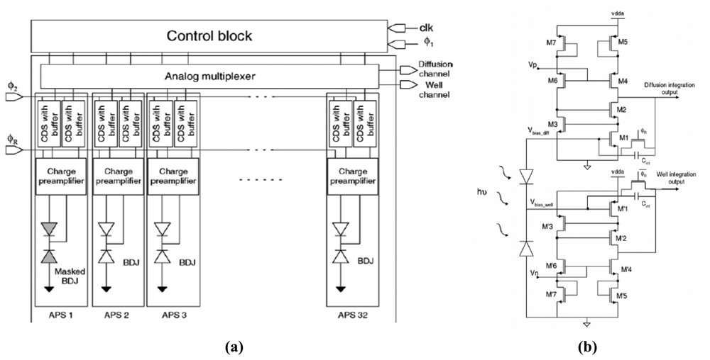
- Carrillo, G.; Lu, G.N.; Pittet, P.; Zhao, K. CMOS BDJ Detector Array with Charge Preamplifiers for Sensitive Biochemical Analysis. In Proc. IEEE ICECS; Nice, France, December 10-13 2006; pp. 367–370. [Google Scholar]
- Simpson, M.L.; Ericson, N.N.; Jellinson, G.E., Jr.; Dress, W.B.; Wintenberg, A.L.; Bobrek, M. Application Specific Spectral Response with CMOS Compatible Photodiodes. IEEE Trans. Electron. Dev. 1999, 46, 905–913. [Google Scholar]
- Gilblom, D.L.; Yoo, S.K.; Ventura, P. Operation and Performance of a Color Image Sensor with Layered Photodiodes. In Proc. SPIE; San Jose, CA, USA, February 15-20 2003; Volume 5074, pp. 318–331. [Google Scholar]
- Billings Merrill, R.; Brehmer, K. Color Separation in an Active Pixel Cell Imaging Array Using a Triple-Well Structure. US Pat.5965875, 1999. [Google Scholar]
- Pinna, A. Conception d'une Rétine Connexionniste: du Capteur au Système de Vision sur Puce. Thesis, University Pierre & Marie Curie, Paris, 2003.
- Green, M.A. Collection Probability Equals Dark Minority Carrier Concentration and Other Surprising Solar Cell Relations. IEEE Photovoltaic Specialists Conf, New York, USA, Sep 29 - Oct 3, 1997; pp. 211–214.
- Green, M.A.; Zhai, J.; Zheng, G.F. High Efficiency Crystalline Silicon Multilayer Solar Cells. In Eur. Photovolt. Solar Ener.Conf. Exhib.; Barcelona, Spain, June 1997. [Google Scholar]
- Brecl, K.; Furlan, J. Modelling Floating Junction Solar Cells. In Proc. Eur. Photovolt. Solar Ener. Conf.; Glasgow, UK, May 2000; Volume 2, pp. 1293–1297. [Google Scholar]
- Brecl, J.; Furlan, K. Modelling Multilayer Semiconductor Structures. In MSM Conf.; San Diego, California, USA, March 27-29 2000; pp. 376–379. [Google Scholar]
- Dierickx, B.; Bogaerts, J. NIR-Enhanced Image Sensor Using Multiple Epitaxial Layer. In Proc. SPIE; Denver, CO, USA, August 1 2004; Volume 5301, pp. 205–212. [Google Scholar]
- El Gamal, A. Trends in CMOS Image Sensor Technology and Design. In Proc. IEEE IEDM; San Francisco, December 8-11 2002; pp. 805–808. [Google Scholar]
- Wang, W.J.; Liu, X.L.; Li, W.; Ren, H.R.; Liang, K.; Han, D.J. A Blue-Violet Enhanced BDJ Photodetector and its Applications in the Probe Chip Measurements of the LEDs for Solid-State Lighting. Sens. Actuat. A 2007, 136, 168–172. [Google Scholar]
- Pauchard, A.; Besse, P.-A.; Popovic, R.S. A Silicon Blue UV Selective Stripe-Shaped Photodiode. Sens. Actuat. A 1999, 76, 172–177. [Google Scholar]
- Pauchard, A.; Furrer, B.; Randjelovic, Z.; Rochas, A.; Manic, D.; Popovic, R.S. Integrated Microsystem for Blue/UV Detection. Sens. Actuat. B 2000, 85, 99–105. [Google Scholar]
- Yotter, R.A.; Warren, M.R.; Wilson, D.M. Optimized CMOS Photodetector Structures for the Detection of Green Luminescent Probes in Biological Applications. Sens. Actuat. B 2000, 103, 43–49. [Google Scholar]
- Yang, F.; Titus, A.H. Integrated Colour Detectors in 0.18-μm CMOS Technology. Electron. Lett. 2007, 43, 1279–1281. [Google Scholar]
- Findlater, K.M. A CMOS Camera Employing a Double Junction Active Pixel. Thesis, University of Edinburgh, 2001.
- Findlater, K.M.; Denyer, P.B.; Hurwitz, J.E.D.; Raynor, J.M.; Renshaw, D. Buried Double Junction Pixel Using Green and Magenta Filters. In Proc. IEEE CCDs & AIS; Santa Clara, CA, June 28-29 1999; pp. 60–64. [Google Scholar]
- Findlater, K.M.; Renshaw, D.; Hurwitz, J.E.D.; Henderson, R.K.; Bailey, T.E.R.; Smith, S.G.; Purcell, M.D.; Raynor, J.M. A CMOS Image Sensor Employing a Double Junction Photodiode. In Proc. IEEE CCDs & AIS; Lake Tahoe, California, Jun 7-9 2001; pp. 60–63. [Google Scholar]
- Malhotra, V. Method of using DC Photocurrent Measurements to Sense Wavelength or Color of Light or to Characterize Semiconductor Materials. US Pat. 5270536, 1993. [Google Scholar]
- Hynecek, J.; Merrill, R.B.; Martin, R.A. Method and apparatus for improving sensitivity in vertical color CMOS image sensors. US Pat. Appl. 20050194653, 2005. [Google Scholar]
- De Graaf, G.; Riedijk, F.R.; Wolffenbuttel, R.F. Colour-Sensor System with Frequency Output and an ISS or I2C Bus Interface. Sens. Actuat. A 1997, 61, 441–445. [Google Scholar]
- De Graaf, G.; Wolffenbuttel, R.F. Smart Optical Sensor Systems in CMOS for Measuring Light Intensity and Colour. Sens. Actuat. A 1998, 67, 115–119. [Google Scholar]
- De Graaf, G.; Wolffenbuttel, R.F. Illumination Source Identification Using a CMOS Optical Microsystem. IEEE Trans. Instrum. Meas. 2004, 53, 238–242. [Google Scholar]
- De Graaf, G.; Wolffenbuttel, R.F. Optical CMOS Sensor for Detection of Light Sources. Sens. Actuat. A 2004, 10, 77–81. [Google Scholar]
- Kolar, A.; Graba, T.; Pinna, A.; Romain, O.; Granado, B.; Ea, T. An Integrated Digital Architecture for Real-Time Reconstruction in VSIP Sensor, Electronics, Circuits and Systems. In Proc. IEEE ICECS; Nice, France, December 10-13 2006; Volume 10, pp. 144–147. [Google Scholar]
- Kolar, A.; Graba, T.; Pinna, A.; Romain, O.; Granado, B.; Belhaire, E. A Multi Shutter Time Sensor for Multispectral Imaging in a Reconstruction Embedded Sensor. In DCIS Conf.; Sevilla, Spain, November 2007.
- Sedjil, M.; Lu, G.N. A Seawater pH Determination Method Using BDJ Detector. Meas. Sci. Technol. 1998, 9, 1587–1592. [Google Scholar]
- Lu, G.N. A Dual-Wavelength Method Using the BDJ Detector and its Application to Iron Concentration Measurement. Meas. Sci. Technol. 1999, 10, 312–315. [Google Scholar]
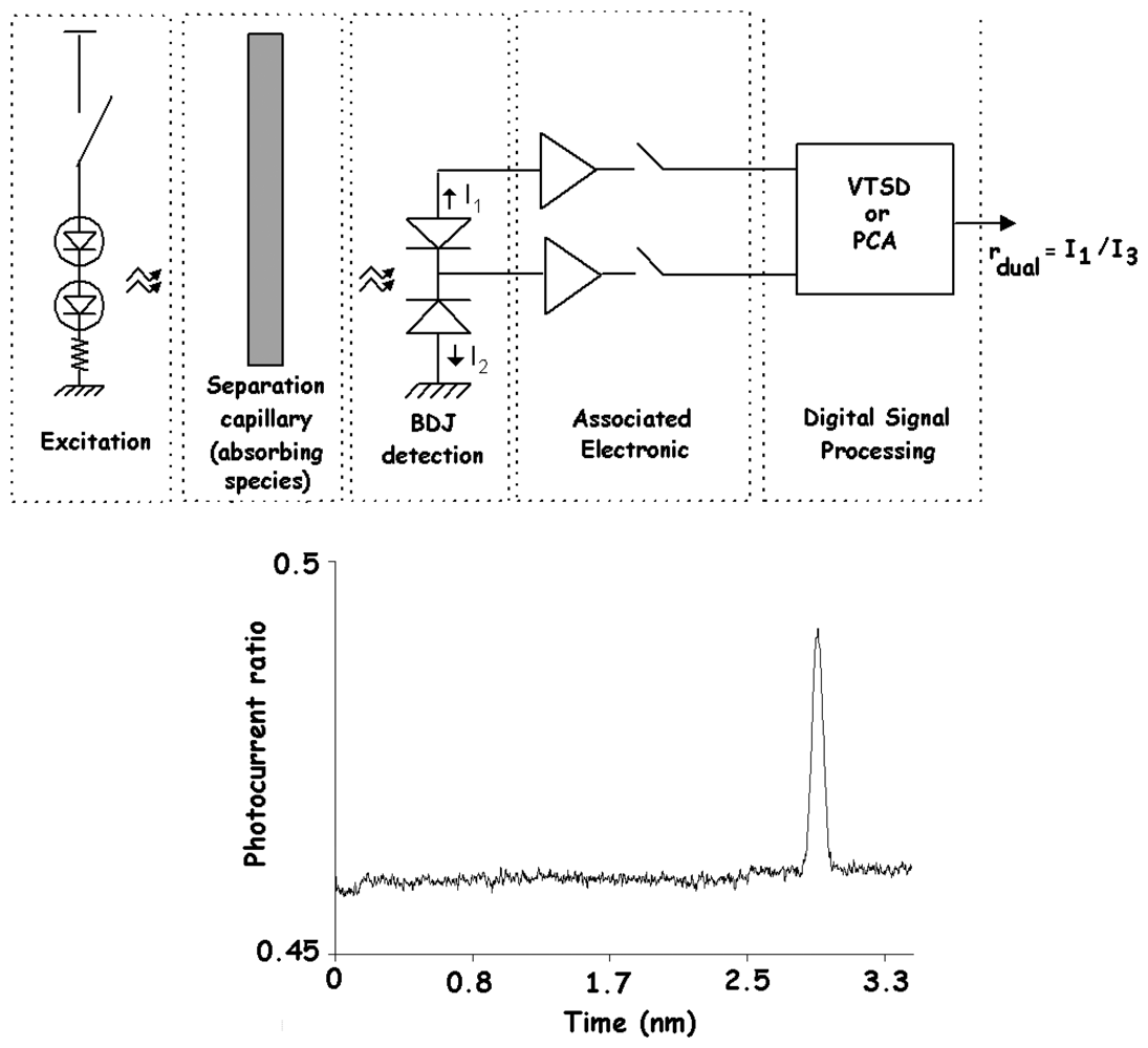
- Pittet, P.; Lu, G. N.; Bertoncini, N.; Renaud, L. CMOS Absorbance Detection System for Capillary Electrophoresis. Mater. Sci. Eng. C 2006, 26, 282–289. [Google Scholar]
- Lu, G.N. A Dual-Wavelength Method Using the BDJ Detector and its Application to Iron Concentration Measurement. Meas. Sci. Technol. 1999, 10, 312–315. [Google Scholar]
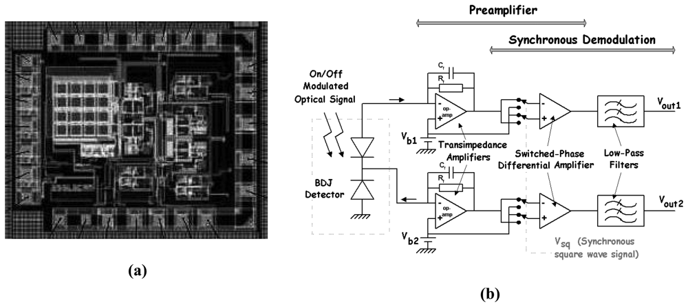
- Lu, G.N.; Pittet, P.; Sou, G.; Carrillo, G.; El Mourabit, A. On-Chip Synchronous Detection for CMOS Detection. In Proc. IEEE ICECS; Croatia, Yugoslavia, September 15-18 2002; pp. 355–358. [Google Scholar]
- Lu, G.N.; Pittet, P.; Sou, G.; Carrillo, G.; El Mourabit, A. A Novel Approach to Implementing On-Chip Synchronous Detection for CMOS Optical Detector Systems. Analog Integr. Circ. S 2003, 37, 57–66. [Google Scholar]
- Pittet, P.; Galvan, J.-M.; Lu, G.N.; Blum, L.J.; Leca-Bouvier, B.D. CMOS LIF Detection System for Capillary Analysis. Sens. Actuat. B 2003, 97, 355–361. [Google Scholar]
- Pittet, P.; Lu, G. N.; El Mourabit, A. On-Chip Transimpedance Preamplifier for CMOS BDJ Optical Detector Using Active Enhanced Impedance Loads. In Proc. IEEE ICECS; Croatia, Yugoslavia, September 15-18 2002; pp. 351–354. [Google Scholar]
- Xu, W.; Mathine, D.L.; Barton, J.K. High-Gain Differential CMOS Transimpedance Amplifier with On-Chip buried Double Junction Photodiode. Electron. Lett. 2006, 42, 803–805. [Google Scholar]
- Wäny, M.; Israel, G.P. CMOS Image Sensor with NMOS-Only Global Shutter and Enhanced Responsivity. IEEE Trans. Electron. Dev. 2003, 50, 57–62. [Google Scholar]


© 2008 by the authors; licensee Molecular Diversity Preservation International, Basel, Switzerland. This article is an open access article distributed under the terms and conditions of the Creative Commons Attribution license (http://creativecommons.org/licenses/by/3.0/).
Share and Cite
Feruglio, S.; Lu, G.-N.; Garda, P.; Vasilescu, G. A Review of the CMOS Buried Double Junction (BDJ) Photodetector and its Applications. Sensors 2008, 8, 6566-6594. https://doi.org/10.3390/s8106566
Feruglio S, Lu G-N, Garda P, Vasilescu G. A Review of the CMOS Buried Double Junction (BDJ) Photodetector and its Applications. Sensors. 2008; 8(10):6566-6594. https://doi.org/10.3390/s8106566
Chicago/Turabian StyleFeruglio, Sylvain, Guo-Neng Lu, Patrick Garda, and Gabriel Vasilescu. 2008. "A Review of the CMOS Buried Double Junction (BDJ) Photodetector and its Applications" Sensors 8, no. 10: 6566-6594. https://doi.org/10.3390/s8106566