Monolithic Active Pixel Sensors (MAPS) in a Quadruple Well Technology for Nearly 100% Fill Factor and Full CMOS Pixels

Abstract
:1. Introduction
2. INMAPS: a quadruple well technology
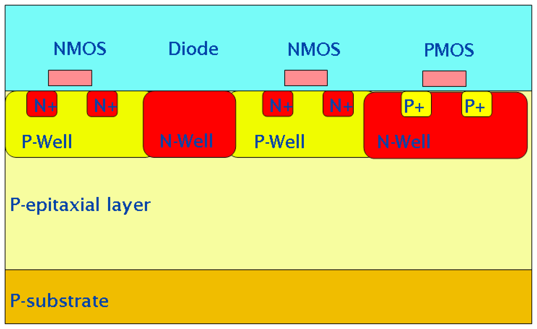
2.1. Standard CMOS
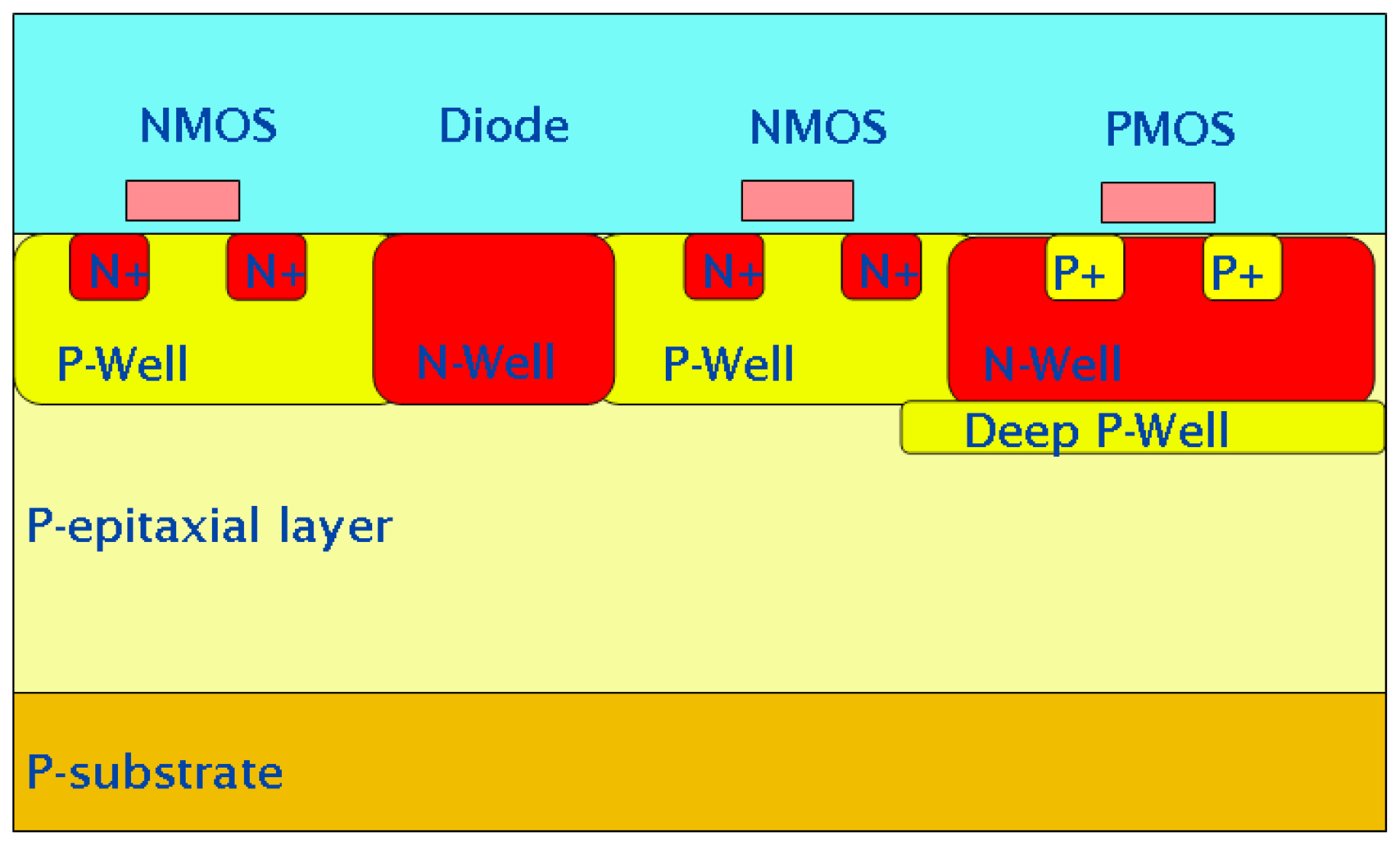
2.2. INMAPS CMOS
3. TPAC1.0: a demonstrator for the INMAPS process
3.1. Application to electromagnetic calorimetry
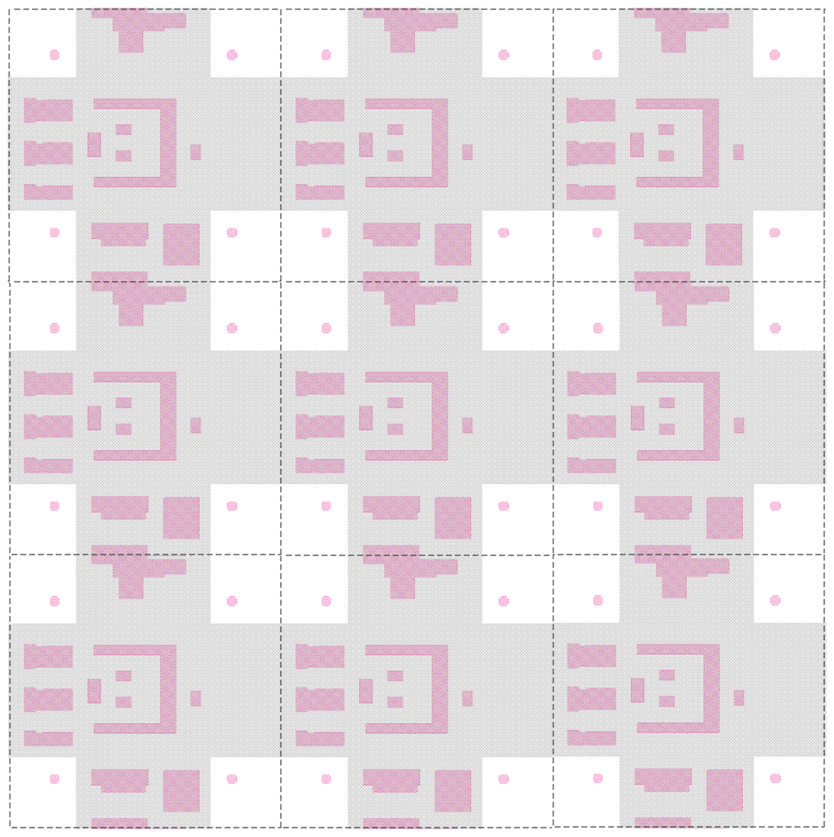
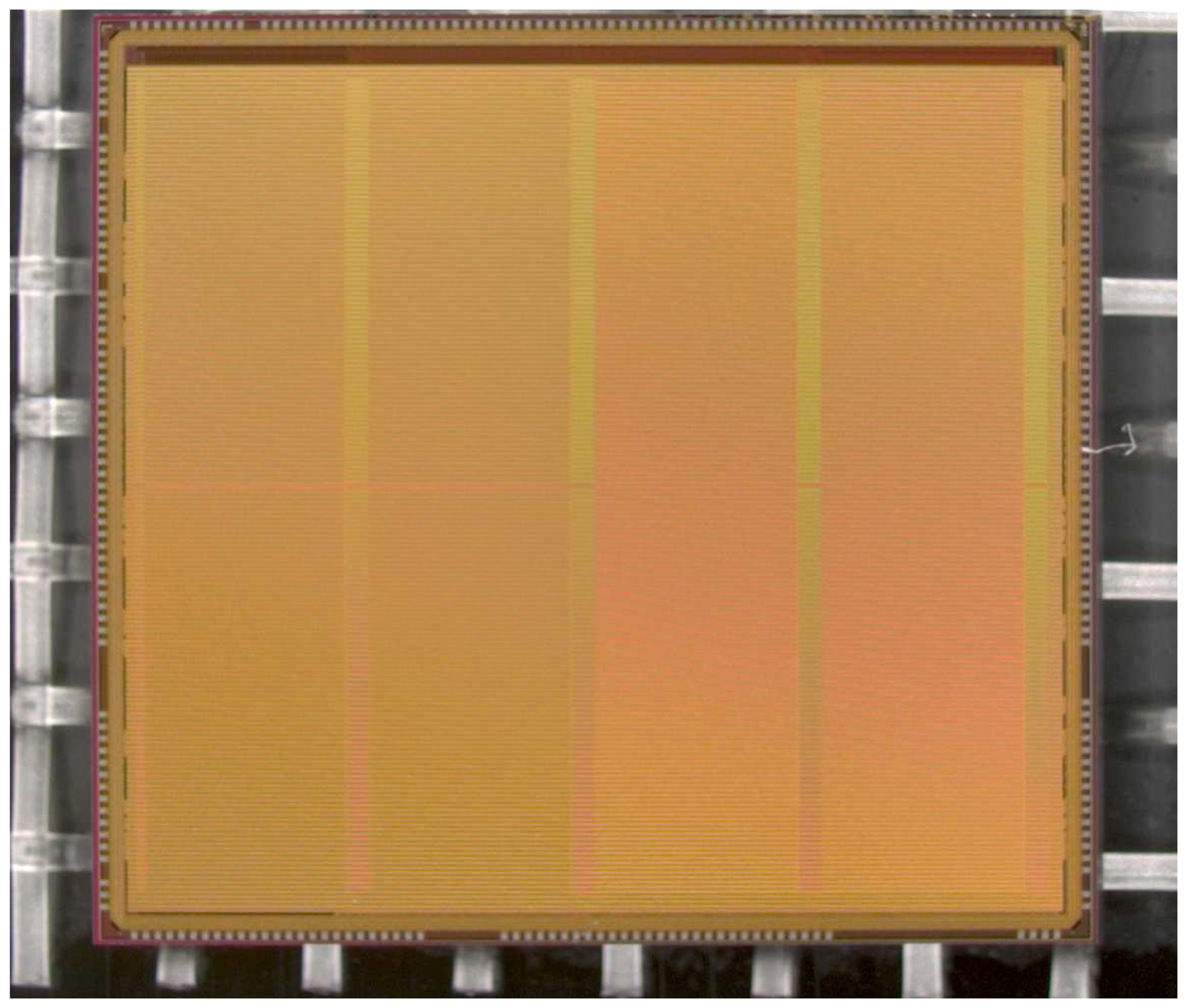
3.2. Sensor design
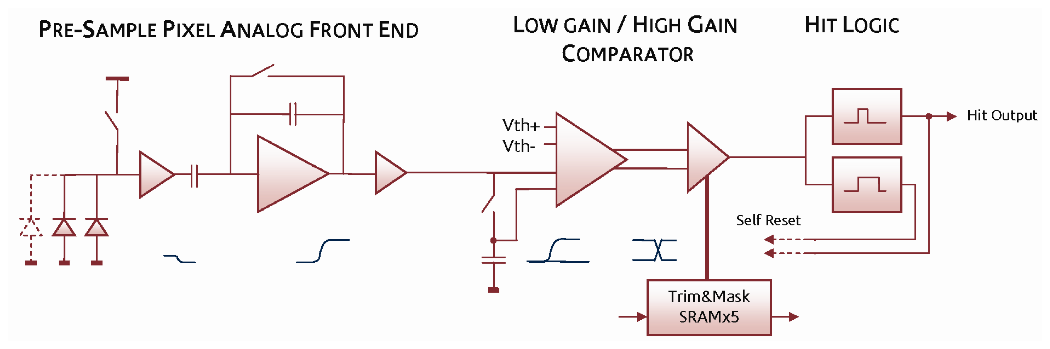
3.3 Sensor Architecture
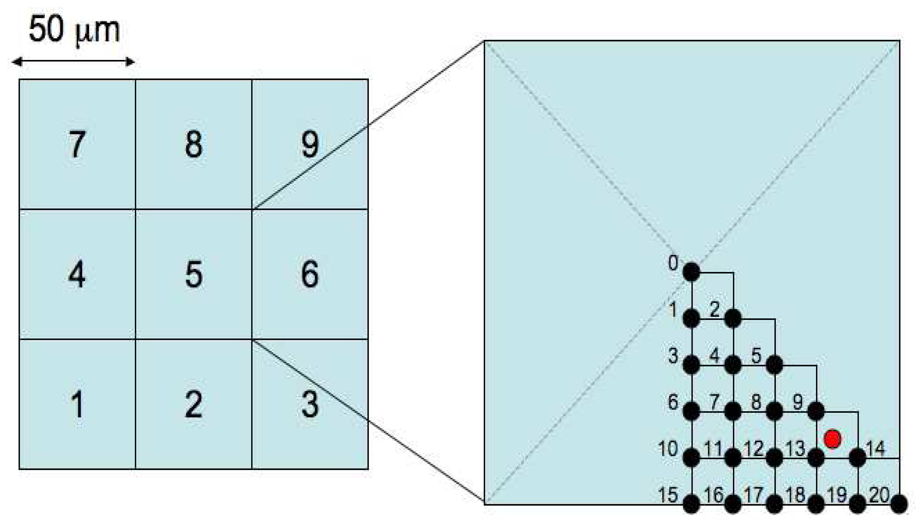
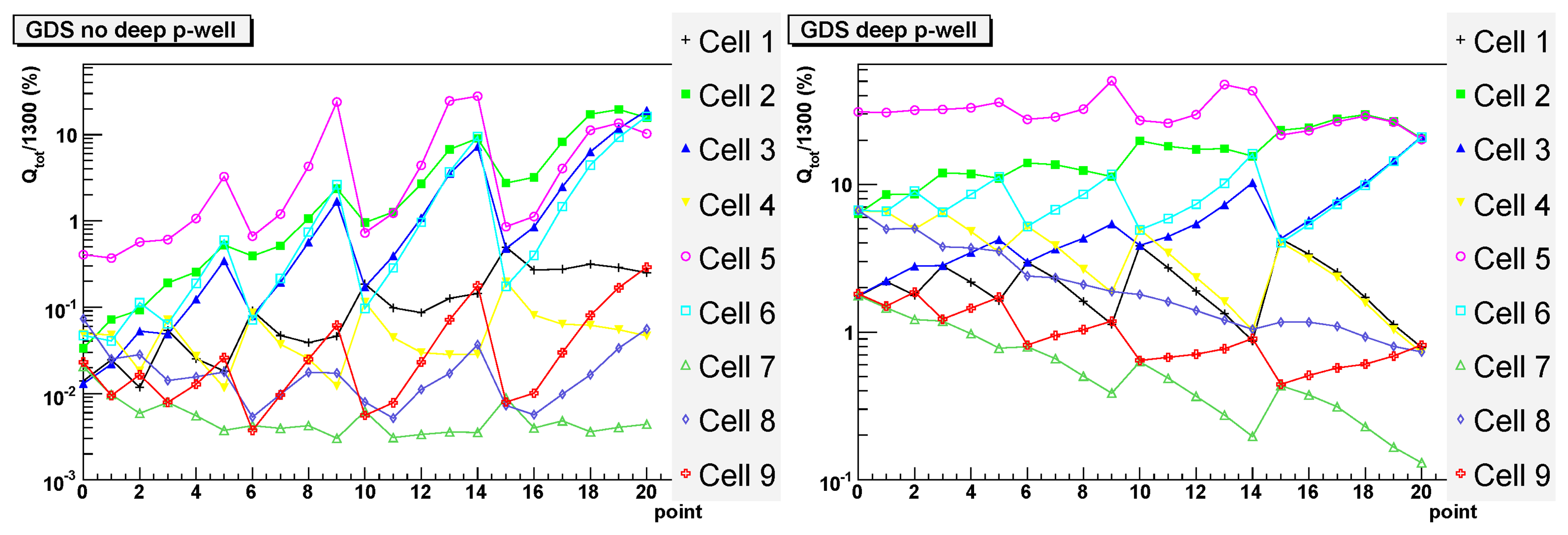
4. The effect of the deep P-well on charge collection efficiency
4.1 Simulation
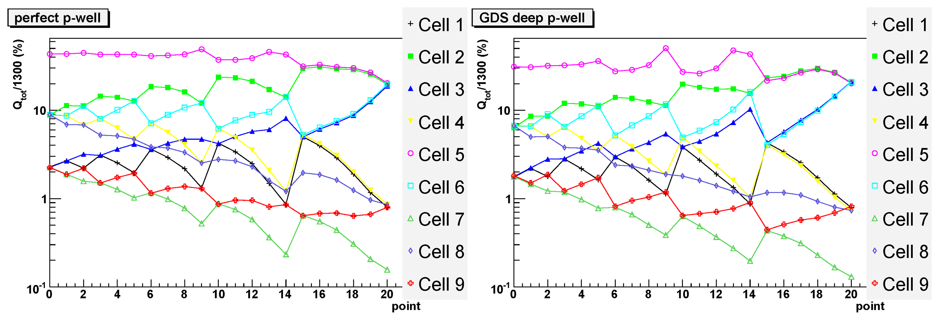
4.2 Experimental results
5. Conclusion
Acknowledgments
References and Notes
- http://www.eetimes.com/news/semi/showArticle.jhtml?articleID=207200173.
- Canon EOS-1Ds Mark III at http://www.canon.com.
- Nikon D700 at http://imaging.nikon.com.
- http://www.aptina.com/.
- Prima, J.; Roy, F.; Coudrain, P.; Gagnard, X.; Segura, J.; Cazaux, Y.; Herault, D.; Virollet, N.; Moussy, N.; Giffard, B.; Gidon, P. A 3 Mega-Pixel Back-Illuminated Image Sensor in 1T5 Architecture with 1.45 mm Pixel Pitch. In Extended Programme of the 2007 International Image Sensor Workshop; Oguinquit, USA, 6-10 June 2007; pp. 5–8. [Google Scholar]
- Cho, S.-H.; Kim, G.; Noh, H.; Moon, C.-R.; Lee, K.; Koh, K.; Lee, D. Optoelectronic Investigation for High Performance 1.4 mm pixel CMOS Image Sensors. In Extended Programme of the 2007 International Image Sensor Workshop; Oguinquit, USA, 6-10 June 2007; pp. 13–15. [Google Scholar]
- Agronov, G.; Mauritzson, R.; Barna, S.; Ladd, J.; Jiang, J.; Dokoutchaev, A.; Fan, X. Super Small, Sub 2 mm Pixels for Novel CMOS Image Sensors. In Extended Programme of the 2007 International Image Sensor Workshop; Oguinquit, USA, 6-10 June 2007; pp. 307–310. [Google Scholar]
- Guidash, R.; Lee, T.; Lee, P.; Sackett, D. A 0.6 μm CMOS pinned photodiode color imager technology. IEDM Tech. Dig. 1997, 927–929. [Google Scholar]
- Kozlowski, L.J.; Rossi, G.; Blanquart, L.; Marchesini, R.; Ying, Huang; Chow, G.; Richardson, J.; Standley, D. Pixel Noise Suppression via SoC Management of Tapered Reset in a 1920×1080 CMOS Image Sensor. IEEE Journal on Solid-State Circuits 2005, 40(12), 2766–2776. [Google Scholar]
- Fowler, B.; Godfrey, M.; Balicki, J.; Canfield, J. Low Noise readout using active reset for CMOS APS. Proceedings SPIE 2000, 3965, 126–135. [Google Scholar]
- Fowler, B.; Godfrey, M.; Mims, S. Reset Noise Reduction in Capacitive Sensors. IEEE Trans. on Circuits and Systems-I 2006, 53(8), 1658–1669. [Google Scholar]
- Arndt, K.; Bolla, G.; Bortoletto, D.; Giolo, K.; Horisberger, R.; Roy, A.; Rohe, T.; Son, S. Silicon sensors development for the CMS pixel system. Nucl. Instruments and Methods in Physics Research A 2003, 511, 106–111. [Google Scholar]
- Gemme, C. The ATLAS pixel detector. Nucl. Instruments and Methods in Physics Research A 2003, 501, 87–92. [Google Scholar]
- Greiner, L.; Matis, H.S.; Ritter, H.G.; Rose, A.; Stezelberger, T.; Sun, X.; Szelniak, M.; Thomas, J.; Vu, C.; Wieman, H. Results from a prototype MAPS sensor telescope and readout system with zero suppression for the heavy flavor tracker at STAR. Nucl. Instruments and Methods in Physics Research A 2008, 589, 167–172. [Google Scholar]
- Heuser, J.M.; Deveaux, M.; Muentz, C.; Stroth, J. Requirements for the Silicon tracking System of CBM at FAIR. Nucl. Instruments and Methods in Physics Research A 2006, 568, 258–262. [Google Scholar]
- Olivo, A.; Arvanitis, C.D.; Bohndiek, S.E.; Clark, A.; Prydderch, M.; Turchetta, R.; Speller, R.D. First evidence of phase contrast imaging with laboratory sources and active pixel sensors. Nucl. Instruments and Methods in Physics Research A 2007, 581(3), 776–782. [Google Scholar]
- Bohndiek, S.E.; Cook, E.J.; Arvantis, C.D.; Olivo, A.; Royle, G.J.; Clark, A.T.; Prydderch, M.L.; Turchetta, R.; Speller, R.D. A CMOS Active pixel sensor system for laboratory-based X-ray diffraction studies of biological tissue. Physics in Medicine and Biology 2008, 53, 655–672. [Google Scholar]
- Faruqi, A.R.; Henderson, R. Electronic detectors in electron microscopy. Curr. Opin. Struct. Biol. 2007, 17(5), 549–555. [Google Scholar]
- Waltham, N.R.; Prydderch, M.; Mapson-Menhard, H.; Pool, P.; Harris, A. Development of a thinned back-illuminated CMOS active pixel sensor for extreme ultraviolet spectroscopy and imaging in space science. Proceedings SPIE 2007, 6690, 702–715. [Google Scholar]
- Dierickx, B.; Meynants, G.; Scheffer, D. Near 100% fill factor CMOS active pixels. In Extended Programme of the 1997 IEEE Workshop on CCD and Advanced Image Sensors; Brugge, Belgium, 6-10 June 1997; pp. 89–93. [Google Scholar]
- Turchetta, R.; Berst, J.D.; Casadei, B.; Claus, G.; Colledani, C.; Dulinski, W.; Hu, Y.; Husson, D.; Le Normand, J.P.; Riester, J.L.; Deptuch, G.; Goerlach, U.; Higueret, S.; Winter, M. A monolithic active pixel sensor for charged particle tracking and imaging using standard VLSI CMOS technology. Nuclear Instruments and Methods A in Physics Research 2001, 458, 677–689. [Google Scholar]
- Deptuch, G.; Winter, M.; Dulinski, W.; Husson, D.; Turchetta, R.; Riester, J.L. Simulation and measurements of charge collection in monolithic active pixel sensors. Nuclear Instruments and Methods A in Physics Research 2001, 465, 92–100. [Google Scholar]
- Peric, I. A novel monolithic pixel detector implemented in high-voltage CMOS technology. Nuclear Science Symposium Conference Record 2007, 2, 1033–1039. [Google Scholar]
- Bulgheroni, A.; Caccia, M.; Domanski, K.; Grabiec, P.; Grodner, M.; Joaroszewicz, B.; Klatka, T.; Kociubinski, A.; Koziel, M.; Kucewicz, W.; Kucharski, K.; Kuta, S.; Marczewski, J.; Niemiec, H.; Sapor, M.; Szelezniak, M.; Tomaszewski, D. Monolithic Active pixel detector realised in silicon on insulator technology. Nuclear Instruments and Methods A in Physics Research 2004, 535, 398–403. [Google Scholar]
- Arai, Y.; Hazumi, M.; Ikegami, Y.; Kohriki, T.; Tajima, O.; Terada, S.; Tsuboyama, T.; Unno, Y.; Ushiroda, H.; Ikeda, H.; Hara, K.; Ishino, H.; Kawasaki, T.; Martin, E.; Varner, G.; Tajima, H.; Ohno, M.; Fukuda, K.; Komatsubara, H.; Ida, J.; Hayashi, H. Monolithic Pixel Detector in a 0.15 μm SOI technology. Nuclear Science Symposium Conference Record 2007, 3, 1440–1444. [Google Scholar]
- Stanitzki, M.; Ballin, J.A.; Crooks, J.P.; Dauncey, P.D.; Magnan, A.M.M.; Mikami, Y.; Miller, O.; Noy, M.; Rajovic, V.; Stefanov, K.D.; Turchetta, R.; Tyndel, M.; Villani, E.G.; Watson, N.K.; Wilson, J.A. A Tera-Pixel Calorimeter for the ILC. Proceedings of the IEEE Symposium on Nuclear Science; 2007; 1, pp. 254–258. [Google Scholar]
- Crooks, J.P.; Ballin, J.A.; Dauncey, P.D.; Magnan, A.-M.; Mikami, Y.; Miller, O.; Noy, M.; Rajovic, V.; Stanitzki, M.; Stefanov, K.D.; Turchetta, R.; Tyndel, M.; Villani, E.G.; Watson, N.K.; Wilson, J.A. A Novel CMOS Monolithic Active Pixel Sensor with Analog Signal Processing and 100% Fill Factor. Proceedings of the IEEE Symposium on Nuclear Science; 2007; 2, pp. 931–935. [Google Scholar]
- Bichsel, H. Straggling in thin silicon detectors. Review of Modern Physics 1988, 60, 663–699. [Google Scholar]
- Sentaurus TCAD. http://www.synopsys.com/products/tcad/tcad.html.


© 2008 by the authors; licensee Molecular Diversity Preservation International, Basel, Switzerland. This article is an open-access article distributed under the terms and conditions of the Creative Commons Attribution license (http://creativecommons.org/licenses/by/3.0/).
Share and Cite
Ballin, J.A.; Crooks, J.P.; Dauncey, P.D.; Magnan, A.-M.; Mikami, Y.; Miller, O.D.; Noy, M.; Rajovic, V.; Stanitzki, M.; Stefanov, K.; et al. Monolithic Active Pixel Sensors (MAPS) in a Quadruple Well Technology for Nearly 100% Fill Factor and Full CMOS Pixels. Sensors 2008, 8, 5336-5351. https://doi.org/10.3390/s8095336
Ballin JA, Crooks JP, Dauncey PD, Magnan A-M, Mikami Y, Miller OD, Noy M, Rajovic V, Stanitzki M, Stefanov K, et al. Monolithic Active Pixel Sensors (MAPS) in a Quadruple Well Technology for Nearly 100% Fill Factor and Full CMOS Pixels. Sensors. 2008; 8(9):5336-5351. https://doi.org/10.3390/s8095336
Chicago/Turabian StyleBallin, Jamie Alexander, Jamie Phillip Crooks, Paul Dominic Dauncey, Anne-Marie Magnan, Yoshiari Mikami, Owen Daniel Miller, Matthew Noy, Vladimir Rajovic, Marcel Stanitzki, Konstantin Stefanov, and et al. 2008. "Monolithic Active Pixel Sensors (MAPS) in a Quadruple Well Technology for Nearly 100% Fill Factor and Full CMOS Pixels" Sensors 8, no. 9: 5336-5351. https://doi.org/10.3390/s8095336