Article

Electrosprayed Metal Oxide Semiconductor Films for Sensitive and Selective Detection of Hydrogen Sulfide

1
LASC Groupe Capteurs, ISEA, University Paul Verlaine-Metz, 7 rue Marconi, 57070 Metz, France
2
Delft Institut for Sustainable Energy, Delft University of Technology, Julianalaan 136, 2628 BL Delft, The Netherlands
*
Author to whom correspondence should be addressed.
Sensors 2009, 9(11), 9122-9132; https://doi.org/10.3390/s91109122
Submission received: 13 October 2009 / Revised: 5 November 2009 / Accepted: 6 November 2009 / Published: 17 November 2009
(This article belongs to the Special Issue Gas Sensors 2009)

Abstract

:
Semiconductor metal oxide films of copper-doped tin oxide (Cu-SnO2), tungsten oxide (WO3) and indium oxide (In2O3) were deposited on a platinum coated alumina substrate employing the electrostatic spray deposition technique (ESD). The morphology studied with scanning electron microscopy (SEM) and atomic force microscopy (AFM) shows porous homogeneous films comprising uniformly distributed aggregates of nano particles. The X-ray diffraction technique (XRD) proves the formation of crystalline phases with no impurities. Besides, the Raman cartographies provided information about the structural homogeneity. Some of the films are highly sensitive to low concentrations of H2S (10 ppm) at low operating temperatures (100 and 200 °C) and the best response in terms of Rair/Rgas is given by Cu-SnO2 films (2500) followed by WO3 (1200) and In2O3 (75). Moreover, all the films exhibit no cross-sensitivity to other reducing (SO2) or oxidizing (NO2) gases.

1. Introduction

The high toxicity of hydrogen sulfide, which has significant negative impacts on health and the environment, has attracted attention to the necessity of monitoring and controlling this gas. With a maximum allowed limit in the atmosphere of 10 ppm H2S, developing reliable sensors with high sensitivity and also selectivity towards other gases is a real challenge. Metal oxide semiconductors (MOS) have been extensively investigated fFor this purpose due to their simplicity, small dimensions and attractive pricepoint. Several types of metal oxide semiconductors [1-3] have been used as sensing material for different type of gases [4-7].
Concerning H2S detection, the literature shows that copper oxide, present in the SnO2 structure, greatly improves the sensitivity towards H2S and the selectivity to some reducing gases [8,9]. Good sensitivity to H2S has also been reported by using tungsten oxide films [10]. In general, other materials can be used for the detection of H2S, and their performance as gas sensors depends mainly on their textural, morphological and structural properties [11,12] and also by the presence of dopants or additives [13-15]. Hence, different techniques [16-18] are used to fabricate films or powders of MOS with desired characteristics which further allows one to achieve good quality sensors.
In this paper the electrostatic spray deposition technique was selected for the preparation of Cu-SnO2, WO3 and In2O3 thin films, due to its advantages such as simplicity and cost-effective set-up, ambient atmosphere operation and easy control of surface morphology by tuning the deposition parameters (temperature, time, flow rate,…). The film deposition process is described along with their morphological and structural characterizations by scanning electron microscopy (SEM), atomic force microscopy (AFM), X-Ray diffraction (XRD) and Raman Spectroscopy. The sensing performance of the films in the detection of H2S are studied as function of the operating temperature in order to determine the maximum response to H2S. In addition, the cross-sensitivity of the films to other possible interfering toxic gases (NO2 and SO2) is evaluated.

2. Results and Discussion

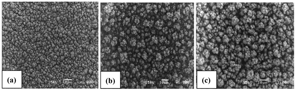
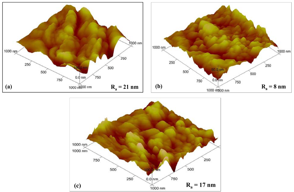
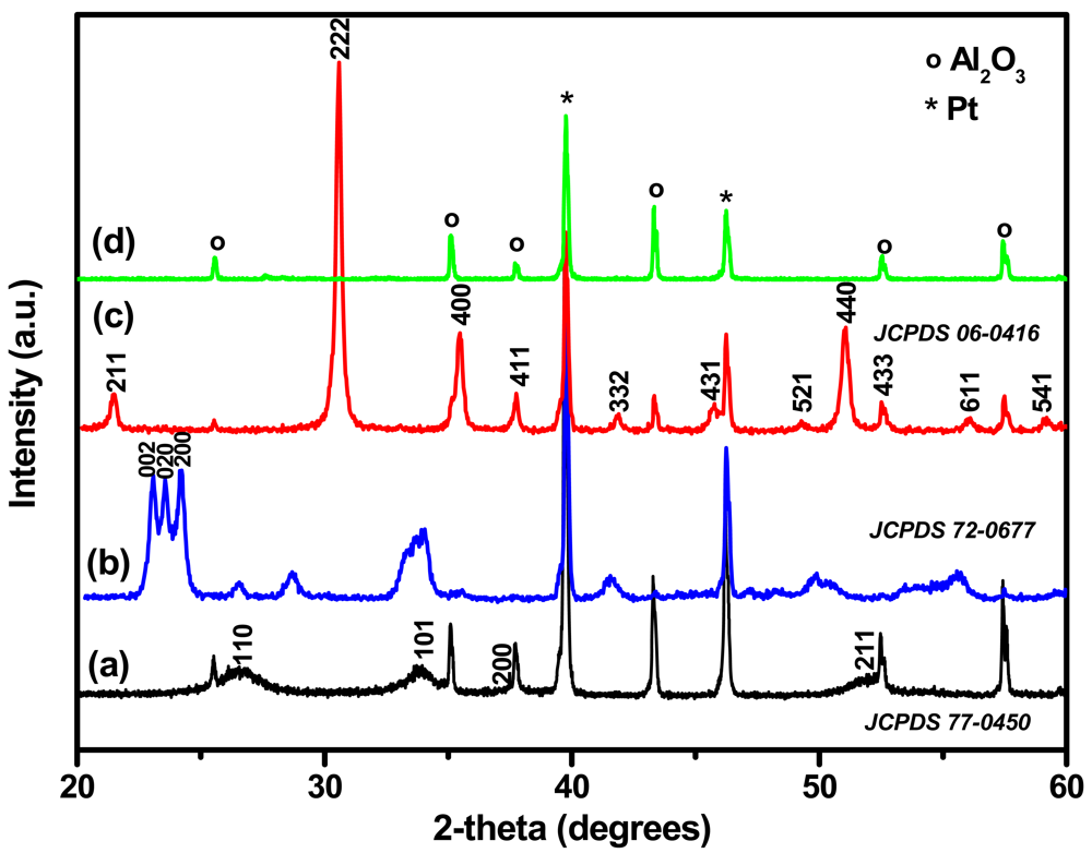
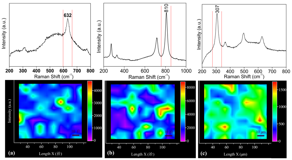
2.1. Morphology and Structure Characterizations

As evaluated by SEM pictures, the morphology of Cu-SnO2, WO3 and In2O3 films presented in Figure 1 shows a porous morphology comprising aggregates with uniform size distribution (2–5 μm for Cu-SnO2 and about 10 μm for In2O3). The WO3 films show variations in the size of the aggregates from 2 μm to 10 μm and this can be due to the lower deposition temperature (350 °C) compared to the deposition temperature of the other films (400 °C). The WO3 films deposited at 400 °C have a more developed porosity than the films prepared at 350 °C, but the adhesion to the substrate was poor, hence, a compromise had to be accepted. The morphology of the films deposited at a certain temperature depends mainly on the rate of evaporation, spreading, precipitation and decomposition reaction. For this reason different deposition parameters has been used for the preparation of the films (Table 1) in order to obtain porous morphology which plays an important role in the adsorption of the gas molecules [19]. The thickness of the films varies from 7 to 10 μm as determined by film cross-section.
Supplementary details about the deposition optimization process of the films are described elsewhere [20-22].
The topographic 3D views of Cu-SnO2, WO3 and In2O3 films are shown in Figure 2. The pictures, realised on a surface of 1 μm per 1 μm, provide information about the shape, the size of the grains and their distribution in the aggregates. Furthermore, by means of appropriate software the mean roughness (Ra) can be calculated. It can be seen that all the films have porous morphology comprising grains with sizes ranging from 100 to 250 nm. The roughness of the Cu-SnO2 seems to be the highest (21 nm), followed by In2O3 (17 nm) and WO3 (7 nm). Hence, no major differences between the films can be noted at this scale.
For a more precise evaluation of the roughness of the films, which could eventually provide a better comparison between the samples, it would be preferable to scan a larger surface. Unfortunately, this could not be successfully accomplished due to the specific morphology of the films, which present cauliflowers-like aggregates that are not connected between them at the surface, so, differences in the height of the aggregates and the “space” between them brought signal instabilities and consequently no good quality pictures could be obtained.
The crystallinity of the films was analysed by the XRD technique, as presented in Figure 3. The films exhibit crystalline phases with peaks corresponding to tetragonal rutile (Cu-SnO2), monoclinic (WO3) and cubic (In2O3) phases [20-22]. No supplementary peaks (except those of the substrate) are detected, proving the purity of the films. The average crystallite sizes are calculated according to Debye-Scherrer formula [23] and are about 7–10 nm for Cu-SnO2 and 20–30 nm for WO3 and In2O3. The small crystallite size of Cu-SnO2 is also suggested by their broad XRD peaks. For gas sensor applications the size of the crystallite is very important since improved sensitivity has been reported for materials which have crystallite size similar to twice of the space charge layer (2L) [12]. In our case the Cu-SnO2 has the closest value to 2L (6 nm).
Supplementary information concerning structural homogeneity of the films was provided by Raman spectroscopy studies. In Figure 4 the Raman spectra and cartographies of Cu-SnO2, WO3 and In2O3 are shown. All the present peaks are indexed to rutile SnO2 [24], monoclinic WO3 [25] and cubic In2O3 [26,27] in good accordance with the literature. Furthermore, these results validate the XRD ones with respect of the phase crystallization. To obtain the Raman cartographies approximately 100 spectra were collected for each film on a surface of 120 μm × 120 μm. The image was further obtained by the integration of the highest peak (632 cm−1 for Cu-SnO2, 810 cm−1 for WO3 and 307 cm−1 for In2O3) in each studied point.
It can be seen that the films are quite homogeneous in structure but they also present variations in the peak intensities which can be perhaps related to their morphology (especially to the grain size) and to the crystallinity. This type of Raman mapping gives an overall view of the surface structure of a material which is advantageous compared to the literature [28] where generally only one Raman spectrum is presented and sometimes the evaluation of a small structural variation is delicate to be exploited.

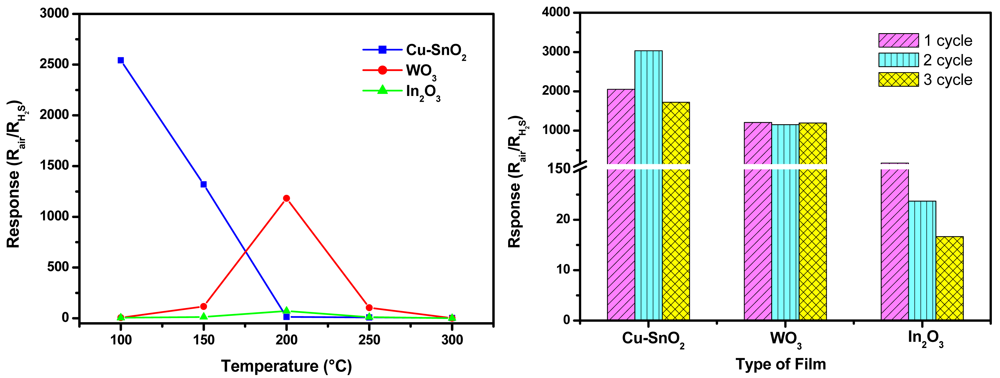
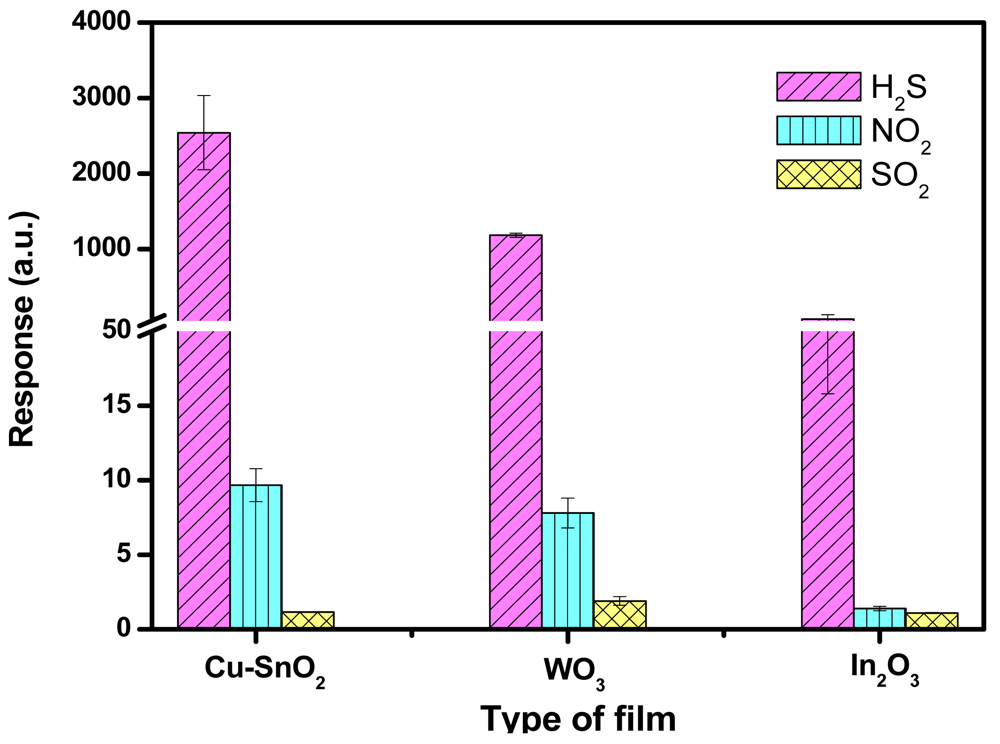
2.2. Gas Sensing Properties

Figure 5a presents the response (Rair/RH2s) of the films to 10 ppm H2S as a function of the operating temperature. The maximum response (2500) is showed by Cu-SnO2 films at 100 °C. At this temperature the other films exhibit low response (about 6). They show better response (1200 for WO3 and 75 for In2O3) than Cu-SnO2 (13) at higher temperature (200 °C).
Comparing to the literature, the Cu-SnO2 prepared in this work presents higher response at lower operating temperature than some other Cu-SnO2 materials fabricated with different techniques [8]. In the same way, the performances of WO3 are superior to those reported in [29]. On the contrary, the response obtained in [10] is higher than that of our films, but with the disadvantage of a recovery process possible only by applying heating pulses at 250 °C. Concerning the In2O3 films in the detection of H2S, there are just few dedicated papers in the literature [30-32], and we can say that our film response is not remarkable.
The differences between the film responses studied in this work can be due to the nature of the studied oxide and their morphological and structural properties. The accepted mechanism for the detection of reducing gases consists in the reaction of chemisorbed oxygen species ( O 2 , O, O2−) on the film surface and the gas molecules (H2S). As a consequence of this reaction the electrons are released, the film resistance decreases (RH2s) and the response is improved. In addition, for Cu-SnO2 the influence of the copper dopant has to be taken into account since without dopant the sensitivity of SnO2 is very low [33]. In this direction several authors have proven by different techniques [34,35] the formation of CuS due to the reaction between Cu or CuO with H2S. The CuS metallic nature (low resistance) allows great sensor response to be achieved. The choice of a proper dopant for WO3 and In2O3 could beneficially improve their performance.
The reproducibility of the film response at their optimum operating temperature (Figure 5b) shows very good and satisfactory values for WO3 and Cu-SnO2, respectively. The In2O3 films present significant response differences between successive gas exposure cycles and this can be due to the incomplete recovery of the film resistance within the selected period of 60 minutes air purging. A good recovery of the resistance and implicitly of the response was be achieved by a long period (one night) of air exposure. Long recovery times for In2O3 have also been reported by other authors [36,37].
The ability of detecting a desired gas from a mixture of gases is an important performance property of a sensor. For Cu-SnO2 the 100 °C optimum temperature was selected to study the cross-sensitivity to other reducing (SO2) and oxidising (NO2) gases, while for WO3 and In2O3 the 200 °C temperature was used. The selection of the temperature corresponds to the temperature offering the maximum response to H2S. As highlighted in Figure 6, all the films present significantly higher response for H2S than for NO2 or SO2. Hence, we can affirm that the films can provide selectivity in an eventually H2S detection from a mixture comprising the three studied gases (H2S, NO2 and SO2).

3. Experimental Section

3.1. Film Deposition Process

The films (Cu-SnO2, WO3 and In2O3) were deposited on Pt partially coated alumina using the ESD technique as presented in Reference [22]. The parameters used for the deposition of the films are described in Table 1. The precursors were dissolved in ethanol in order to obtain a 0.05 M solution which was atomisated by applying a high voltage (7-8 kV) between a metallic nozzle and a heated and grounded substrate. The formed aerosol (spray) comprises highly charged droplets which are directed to the substrate under an electrostatic force. At the impact, the droplets loose their charge, and then spreading, drying, and decomposition of the precursor solution occur. In this way a thin layer was formed on the substrate surface and to improve their crystallinity annealing treatment was performed. Several films of each composition have been prepared to validate the reproducibility of film deposition in terms of morphology, structure, homogeneity, and gas responses.

3.2. Characterization Techniques

The film morphology was studied using a JOEL JSM 580LV scanning electron microscope and the topography was evaluated with an atomic force microscope (Nanoscope IV-Multimode Veeco Instruments, USA) operating in a tapping mode regime. Raman measurements were performed at room temperature using a Jobin-Yvon microspectometer having a He-Ne excitation source (wavelength 632.8 nm). The sample surface was visualized by an optical microscope which allowed the selection of specific zone for structure evaluation. Raman spectra were recorded by scanning a part of the sample surface (120 μm × 120 μm) in 10 μm steps in both X and Y-axes. By integration of the desired Raman peak, the structural cartography of the surface was obtained.

3.3. Sensing Measurements

The gas sensing measurements were carried out in a closed quartz tube furnace. The temperature was measured using a type K thermocouple and was controlled by a PID temperature regulator (JUMO dTRON 16.1). The resistance measurements were performed using a two-point probe method with an electrometer (KEITHLEY 6514). The gas response of a film (S) is defined as the ratio of Rair/Rgas for H2S and SO2 (reducing gases) and Rgas/Rair for NO2 (oxidizing gas), where Rair represents the electrical resistance of the film in synthetic air and Rgas represents the resistance during the gas exposure.
To determine the temperature at which the H2S response was maximum, the films were exposed to 10 ppm H2S in a temperature range of 100 to 300 °C. Firstly the temperature was set to the desired value and the films were purged with synthetic air for 60 min. Next, the films were exposed to H2S for 30 min, followed by regeneration with synthetic air for 60 min. This cycle was repeated about four times during a day (in order to ensure the reproducibility). The responses of the films to 20 ppm SO2 and 1 ppm NO2 were evaluated at the selected operating temperature (temperature at which the film shows the maximum response).
The concentration of gases was fixed by adjusting the flow rates of a target gas and a carrier gas (synthetic air) in the way to maintain a constant total flow rate of 100 mL/min. The gas bottles were provided by Air Products (France) and the concentration of the gases was controlled using mass flow controllers (MFC, BROOKS Instruments, 5850 TR).

4. Conclusions

This paper describes the deposition of metal oxide semiconductor films of Cu-SnO2, WO3 and In2O3 using the electrostatic spray deposition technique and their use in the detection of hydrogen sulfide. It has been shown that this simple and cost-effective technique allows the fabrication of films with desired characteristics for gas sensor applications, i.e., porous and homogeneous morphology, good crystallinity, crystallite size in the nanometer range and purity. These highlighted characteristics can afford a high sensitivity of our films to H2S with a maximum response achieved by Cu-SnO2 (2,500) and followed by WO3 (1,200) and In2O3 (75). In addition, their low operating temperatures (100 °C and 200 °C) makes them attractive from a practical and energy economy point of view. For measurements in real atmospheres, several gases can be present at the same time, so, the selectivity of a sensor is crucial in order to avoid interferences between different gases. With respect of this aspect no cross-sensitivity of all the studied films to SO2 or NO2 was found.

Acknowledgments

The authors would like to acknowledge Dr. Cathie Vix from the Institut de Science des Matériaux de Mulhouse (France) for the characterization technique facilities and also to Dr. Viorela Ostaci for the collaboration in the AFM technique.

References and Notes

  1. Barratto, C.; Sberveglieri, G.; Onischuk, A.; Caruso, B.; di Stasio, S. Low temperature selective NO2 sensors by nanostructured fibres of ZnO. Sens. Actuat. B 2004, 100, 261–265. [Google Scholar]
  2. Barret, E.P.S.; Georgiades, G.C.; Sermon, P.A. The mechanism of operation of WO3-based H2S sensors. Sens. Actuat. 1990, B1, 116–120. [Google Scholar]
  3. Cobianu, C.; Savaniu, C.; Siciliano, P.; Capone, S.; Utriainen, M.; Niinisto, L. SnO2 sol-gel derived thin films for integrated gas sensors. Sens. Actuat. B 2001, 77, 496–500. [Google Scholar]
  4. Bender, F.; Kim, C.; Mlsna, T.; Vetelino, J.F. Characterization of a WO3 thin film chlorine sensor. Sens. Actuat. B 2001, 77, 281–286. [Google Scholar]
  5. Comini, E.; Faglia, G.; Sberveglieri, G. CO and NO2 response of tin oxide silicon doped thin films. Sens. Actuat. B 2001, 76, 270–274. [Google Scholar]
  6. Galatsis, K.; Li, Y.X.; Wlodarski, W.; Kalantar-Zadeh, K. Sol-gel prepared MoO3-WO3 thin-films for O2 gas sensing. Sens. Actuat. B 2001, 77, 478–483. [Google Scholar]
  7. Ivanovskaya, M.; Gurlo, A.; Bogdanov, P. Mechanism of O3 and NO2 detection and selectivity of In2O3 sensors. Sens. Actuat. B 2001, 77, 264–267. [Google Scholar]
  8. Liu, J.; Huang, X.; Ye, G.; Liu, W.; Jiao, Z.; Chao, W.; Zhou, Z.; Yu, Z. H2S detection sensing characteristic of CuO/SnO2 sensor. Sensors 2003, 3, 110–118. [Google Scholar]
  9. Rumyantseva, M.N.; Labeau, M.; Senateur, J.P.; Delabouglise, G.; Boulova, M.; Gasckov, A.M. Influence of copper on sensor properties of tin dioxide films in H2S. Mater. Sci. Eng., B 1996, 41, 228–234. [Google Scholar]
  10. Solis, J.L.; Saukko, S.; Kish, L.B.; Granqvist, C.G.; Lantto, V. Nanocrystalline tungsten oxide thick-film with high sensitivity to H2S at room temperature. Sens. Actuat. B 2001, 77, 316–321. [Google Scholar]
  11. Ruiz, A.M.; Sakai, G.; Cornet, A.; Shimanoe, K.; Morante, J.R.; Yamazoe, N. Microstructure control of thermally stable TiO2 obtained by hydrothermal process for gas sensors. Sens. Actuat. B 2004, 103, 312–31. [Google Scholar]
  12. Xu, C.; Tamaki, J.; Miura, N.; Yamazoe, N. Grain size effects on gas sensitivity of porous SnO2-based elements. Sens. Actuat. B 1991, 3, 147–155. [Google Scholar]
  13. Paraguay, D.F.; Miki-Yoshida, M.; Morales, J.; Solis, J.; Estrada, L.W. Influence of Al, In, Cu, Fe and Sn dopants on the response of thin film ZnO gas sensor to ethanol vapour. Thin Solid Films 2000, 373, 137–140. [Google Scholar]
  14. Penza, M.; Martucci, C.; Cassano, G. NOx gas sensing characteristics of WO3 thin films activated by noble metals (Pd, Pt, Au) layers. Sens. Actuat. B 1998, 50, 52–59. [Google Scholar]
  15. Steffes, H.; Imawan, C.; Solzbacher, F.; Obermeier, E. Enhancement of NO2 sensing properties of In2O3-based thin film using an Au or Ti surface modification. Sens. Actuat. B 2001, 78, 106–112. [Google Scholar]
  16. Supothina, S. Gas sensing properties of nanocrystalline SnO2 thin films prepared by liquid flow deposition. Sens. Actuat. B 2003, 93, 526–530. [Google Scholar]
  17. Tanaka, S.; Esaka, T. High NOx Sensitivity of oxide thin films prepared by RF sputtering. Mater. Res. Bull. 2000, 35, 2491–2502. [Google Scholar]
  18. Zayim, E.O.; Liu, P.; Lee, S.-H.; Tracy, C.E.; Turner, J.A.; Pitts, J.R.; Deb, S.K. Mesoporous sol-gel WO3 thin films Via Poly(Styrene-Co-Allyl-Alcohol) copolymer templates. Solid State Ionics 2003, 165, 65–72. [Google Scholar]
  19. Safonova, O.V.; Delabouglise, G.; Chenevier, B.; Gaskov, A.M.; Labeau, M. CO and NO2 gas sensitivity of nanocrystalline tin dioxide thin films doped with Pd, Ru and Rh. Mater. Sci. Eng., C 2002, 21, 105–11. [Google Scholar]
  20. Matei Ghimbeu, C.; Schoonman, J.; Lumbreras, M. Porous indium oxide films deposited by electrostatic spray deposition technique. Ceram. Int. 2008, 34, 95–100. [Google Scholar]
  21. Matei Ghimbeu, C.; Van Landschoot, R.C.; Schoonman, J.; Lumbreras, M. Tungsten trioxide thin films prepared by electrostatic spray deposition technique. Thin Solid Films 2007, 515, 5498–5504. [Google Scholar]
  22. Matei Ghimbeu, C.; Van Landschoot, R.; Schoonman, J.; Lumbreras, M. Preparation and characterization of SnO2 and Cu-doped SnO2 thin films using electrostatic spray deposition (ESD). J. Eur. Ceram. Soc. 2007, 27, 207–213. [Google Scholar]
  23. Tunstall, D.P.; Patou, S.; Liu, R.S.; Kao, Y.H. Size effects in the NMR of SnO2 powders. Mater. Res. Bull. 1999, 34, 1513–1520. [Google Scholar]
  24. Yu, K.N.; Xiong, Y.; Liu, Y.; Xiong, C. Microstructural change of nano-SnO2 grain assemblages with the annealing temperature. Phys. Rev. B 1997, 55, 2666–2671. [Google Scholar]
  25. Moulzolf, S.C.; LeGore, L.J.; Lad, R.J. Heteroepitaxial growth of tungsten oxide films on sapphire for chemical gas sensors. Thin Solid Films 2001, 400, 56–63. [Google Scholar]
  26. Rojas-Lopez, M.; Nieto-Navarro, J.; Rosendo, E.; Navarro-Contresas, H.; Vidal, M.A. Raman scattering study of photoluminiscent spark-processed porous InP. Thin Solid Films 2000, 379, 1–6. [Google Scholar]
  27. Vigreux, C.; Binet, L.; Gourier, D. Formation by laser impact of conducting -Ga2O3-In2O3 solid solution with composition gradients. J. Solid State Chem. 2001, 157, 94–101. [Google Scholar]
  28. Habazaki, H.; Hayashi, Y.; Konno, H. Characterization of electrodeposited WO3 films and its application to electrochemical wastewater treatment. Electrochim. Acta 2002, 47, 4181–4188. [Google Scholar]
  29. Reyes, L.F.; Hoel, A.; Saukko, S.; Heszler, P.; Lantto, V.; Granqvist, C.G. Gas sensor response of pure and activated WO3 Nanoparticle films made by advanced reactive gas deposition. Sens. Actuat. B 2006, 117, 128–134. [Google Scholar]
  30. Niu, X.; Zhong, H.; Wang, X.; Jiang, K. Sensing properties of rare earth oxide doped In2O3 by sol-gel method. Sens. Actuat. B 2006, 115, 434–438. [Google Scholar]
  31. Xu, J.; Wang, X.; Shen, J. Hydrothermal synthesis of In2O3 for detecting H2S in air. Sens. Actuat. B 2006, 115, 642–646. [Google Scholar]
  32. Tomchenko, A.A.; Harmer, G.P.; Marquis, B.T.; Allen, J.W. Semiconducting metal oxide sensor array for the selective detection of combustion gases. Sens. Actuat. B 2003, 93, 126–134. [Google Scholar]
  33. Matei Ghimbeu, C.; Lumbreras, M.; Siadat, M.; Landschoot, R.C.; Schoonman, J. Electrostatic sprayed SnO2 and Cu-doped SnO2 films for H2S detection. Sens. Actuat. B 2008, 133, 694–698. [Google Scholar]
  34. Niranjan, R.S.; Patil, K.R.; Sainkar, R.S.; Mulla, I.S. High H2S-sensitive copper-doped tin oxide thin film. Mater. Chem. Phys. 2002, 80, 250–256. [Google Scholar]
  35. Pagnier, T.; Boulova, M.; Galerie, A.; Gaskov, A.; Lucazeau, G. Reactivity of SnO2-CuO nanocristalline materials with H2S: a coupled electrical and Raman spectroscopic study. Sens. Actuat. B 2000, 71, 134–139. [Google Scholar]
  36. Kapse, V.D.; Ghosh, S.A.; Chaudhari, G.N.; Raghuwanshi, F.C.; Gualwade, D.D. H2S sensing properties of La-doped nanocrystalline In2O3. Vacuum 2008, 83, 346–352. [Google Scholar]
  37. Kaur, M.; Namrata, J.; Sharme, K.; Bhattachrya, S.; Roy, M.; Tyagi, A.K.; Gupta, S.K.; Yakhmi, J.V. Room-temperature H2S gas sensing at ppb level by single crystal In2O3 whiskers. Sens. Actuat. B 2008, 133, 456–461. [Google Scholar]
Figure 1. SEM pictures of (a) Cu-SnO2 (b) WO3 and (c) In2O3 films.
Sensors 09 09122f1
Figure 2. 3D AFM topographies of (a) Cu-SnO2 (b) WO3 and (c) In2O3 films.
Sensors 09 09122f2
Figure 3. XRD patterns of (a) Cu-SnO2 (b) WO3 (c) In2O3 films and (d) Pt-Al2O3 substrate.
Sensors 09 09122f3
Figure 4. Raman spectra and cartographies of (a) Cu-SnO2 (b) WO3 and (c) In2O3 films.
Sensors 09 09122f4
Figure 5. (a) Responses to 10 ppm H2S of Cu-SnO2, WO3 and In2O3 as a function of operating temperature and (b) Reproducibility of the film response to 10 ppm H2S at their optimum operating temperature.
Sensors 09 09122f5
Figure 6. Responses of Cu-SnO2, WO3 and In2O3 to 10 ppm H2S, 1 ppm NO2 and 20 ppm SO2 at their optimum operating temperature.
Sensors 09 09122f6
Table 1. Experimental parameters used for the film deposition.
Film TypePrecursorDeposition Temperature (°C)Deposition Time (h)Flow Rate (mL/h)Annealing Temperature (°C)
Cu-SnO2
(1% Cu)
SnCl4·4H2O
Cu(NO3)2·2.5H2O
40012550
WO3W(C2H5O)635011500
In2O3InCl340011.5500

