1. Introduction
Light is reflected when traveling through a boundary between materials with different refractive indices (refractive index of materials A > B). At a critical angle of incidence, the light is reflected with near perfection, producing total internal reflection (TIR), a simple physical phenomena with important practical consequences for biosensing. Planar optical waveguides are comprised of an optically transparent guiding layer with a refractive index that is higher than the substrate layers. With careful selection of the guiding material, and gratings for incoupling of light, biosensors based on planar optical waveguides can provide versatile and robust transduction sensor platforms for the rapid and sensitive analysis of complex environmental and medical samples. Planar waveguide geometries also allow for facile integration with sample delivery and detection systems, and for the functionalization and patterning of arrays of recognition elements onto the surface, allowing for simultaneous detection of multiple analytes using a single waveguide transducer [
1,
2].
When excitation light is coupled into the guiding layer of a planar optical waveguide, light is guided over long distances by TIR. Although most of the light is confined within the guiding layer, a small portion (the evanescent field) extends out into the substrate and into the medium (the biological sample). This evanescent field falls off exponentially as the distance from the waveguide surface increases, and is effectively zero at a distance less than one-half the wavelength of the coupled light. Thus sensitivity is highly enhanced because of the large degree of discrimination between surface bound molecules and contaminants within the sample solution. Evanescent field sensing can be applied to several different transduction approaches including evanescent fluorescence detection, monitoring of refractive index changes or detecting spectroscopic shifts. The current manuscript will largely focus on fluorescence-based detection platforms, with brief discussions on other transduction approaches.
Waveguide sensor systems have been the subject of a large number of investigations over the last two decades. The concept of evanescent field sensing was initially reported by Lukosz and Tiefenthaler in 1983 [
3,
4]. While using thin, high refractive index SiO
2-TiO
2, waveguides with incoupling gratings, they discovered variations in incoupling angles due to changes in the effective refractive index of the guided modes due to variations in humidity. Subsequently, these authors proposed and demonstrated application of this observed effect toward chemical, and biochemical sensing [
3]. Evanescent field sensing is now well established and sensor systems based on both single mode and multimode waveguide structures have been developed and demonstrated by numerous investigators. The physical properties of planar optical waveguides that make them ideal for biosensing applications are discussed in detail below (Section 3). Examples of commercialized technologies as well as new technologies under development are discussed in Section 7.
There are two major classifications of waveguide systems- multimode and single mode. Multimode waveguides have a thickness much greater than the wavelength of the excitation light and are typically fabricated using glass, polymer or silica materials making them relatively inexpensive and easy to manufacture. The thickness of the waveguide is on the order of several microns allowing simple edge coupling of excitation light into the waveguide structure. Unfortunately, due to relatively low levels of signal intensity, detection methods for florescence-based, multimode sensors, typically rely on Peltier-cooled CCD cameras.
Single mode waveguides are typically comprised of a very thin (< wavelength of excitation) high dielectric index film (e.g., silicon oxynitride, tantalum pentoxide and others) deposited on a low index substrate [
5]. The films are typically fabricated using thin film deposition techniques. Alternative fabrication approaches include the use of sol gels [
6] and ion deposition methods. Details on thin film, single mode, planar waveguide design and fabrication are presented in Section 2. Single mode waveguides with large index differences between the film and substrate (high contrast waveguide systems) offer greater sensitivity due to the high field intensity at the surface. Additionally, single mode planar waveguide supports several thousand reflections per centimeter of beam propagation for visible wavelengths, two orders of magnitude higher than multimode planar and fiber waveguides. Finally, single mode planar waveguides with high contrast enable the rapid decay of the evanescent field away from the waveguide surface with no appreciable intensity beyond one-half the wavelength of the excitation light (∼250–300 nm), while low contrast multi-mode configurations typically exhibit a penetration depth of 1–2 microns. As a result, the strong spatial filtering effect further enhances sensitivity by minimizing background from interferents and allows direct analysis of complex samples while eliminating the need for additional rinsing and drying steps. The requirements for highly sensitive detectors are also decreased allowing for use of room temperature based CCD cameras or miniature fiber optic spectrometer systems. However, this increased sensitivity for single mode waveguides requires certain modifications of the waveguide such as thin film deposition and use of grating couplers to couple excitation light into the waveguide films. Another potential problem includes photo-bleaching effects when fluorescent organic dyes are employed for detection due to the strong field intensity at the waveguide surface. However, this problem can be minimized or eliminated by the use of photostable quantum dots (QDs) as fluorescence reporters. Exploiting the broad Stokes shift of these nanoparticles allows for the simultaneous excitation of multiple QDs at a single wavelength, which can be exploited for multiplex detection of analytes on waveguide-based platforms (Section 6).
Incoupling of light into waveguides can be achieved by end-fire coupling or with the use of gratings. Because single-mode waveguide films tend to be thin, on the order of 0.1μm for devices with high sensitivity, end fire coupling is impractical. While this technique works well with waveguides having large core waveguide dimensions, it requires frequent change of the sensor wafer precluding its use in practical applications. This change is necessitated by a requirement of precise XYZ alignment tolerances for efficient coupling and end face preparation of single mode waveguides. The use of grating couplers will be discussed in Section 2.
In this review, we will present the basic physical and optical principles of single mode planar optical waveguides that make them suitable for biosensing applications. We will review the current methods for waveguide-surface functionalization to make them compatible for biological assays, while discussing the different biological sensing applications for which they have been used. We will discuss a waveguide-based biosensor developed by our team at the Los Alamos National Laboratory (LANL) and the adaptation of this technology to biosensing applications in single and multiplex formats. We will also present some commercial applications of waveguides in biosensing. It is impossible to incorporate detailed description of all waveguide-based sensing technologies into a single review article and yet, do justice to them. Therefore, this review article will limit itself to the described scope. Some novel technologies such as silicon photonic biosensors, that have made tremendous impact on such applications will only be briefly discussed, but have been reviewed in detail elsewhere [
7].
2. Waveguide Design and Fabrication
2.1. Waveguiding Principles
Planar optical waveguides are based on a thin, optically transparent film with a refractive index that is higher than adjacent substrate and superstrate mediums. Under this condition, light coupled into the thin waveguide film will be confined to that layer and can propagate over useful distances. Furthermore, the planar waveguide configuration offers important advantages as optical elements may be integrated into or onto the waveguide film surface to form integrated optical circuits, which are thin film analogs of bulk optical circuits [
8]. The telecommunication industry quickly adopted the planar waveguide optical technology due to emerging demands for greater bandwidth and freedom from electromagnetic interference. Similarly, in the early 1980s, the potential for sensing physical and chemical or biological parameters was recognized, resulting in rapid surge in interest in the sensing arena. Successful application of the planar optical waveguide technology is, however, strongly dependent on proper waveguide design. In the following sections waveguide operation and fabrication are discussed and designs for optimized waveguide structures are then presented in later sections (Sections 3 and 6).
For modeling and analysis purposes, an optical waveguide may be described quantitatively using a dispersion relationship incorporating the step index waveguide parameters n
f (film index), n
c (cover film index), n
s (substrate index), and W (waveguide film thickness) [
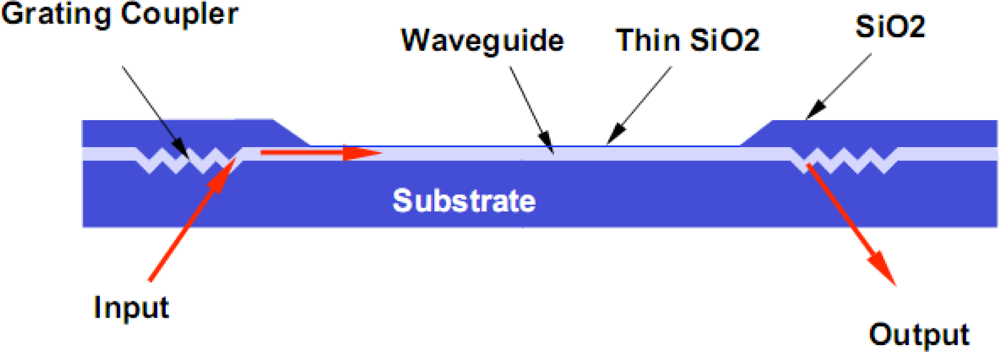
9]. A convenient model for describing waveguiding and defining it’s sensing capability is based on a “zig-zag” optical ray model for the reflection of an optical ray between the two dielectric waveguide surface boundaries as shown in
Figure 1. The dispersion relationship is defined by the “transverse resonance condition”, which requires the sum of all phase shifts perpendicular to the direction of propagation in the waveguide to be a multiple of 2π̣ (2mπ, where m = 0, 1, 2,...) for one “zig-zag” period of the light propagating within the waveguide. Thus, the total phase shift associated with the transverse motion between the two boundaries must be an integer multiple of 2π for each full cycle. For one transverse passage through the waveguide, a phase shift of kn
fWcosθ occurs (k = 2π/λ). One full period, however, requires two transverse passages. Additionally, phase shifts of −2γ
c and −2γ
s occur due to total internal reflection at the cover and substrate boundaries of the waveguide. Thus an equation of the following form results:
Because the waveguide is thin and the index differences are small, waveguiding occurs only at discrete values of θ with each discrete angle corresponding to a propagating mode. Waveguides with propagation at only one specific value of θ are referred to as single mode waveguides while those with propagation at more than one value of θ are described as multimode.
The term n
f Sinθ is defined as the “effective mode index” (N
eff) and represents an effective refractive index that is characteristic of the waveguide material system and configuration. The basis for this definition is illustrated graphically in the plot of the electric field distribution of a single mode waveguide shown in
Figure 1. Associated with a guided optical wave is an exponentially decaying electric field distribution, the evanescent field, extending into the cover and substrate medium. The 1/e penetration depth of the evanescent electric field into the substrate (W
s) and cover medium (W
c) may be defined using the following equations:
It is the interaction of the evanescent field with the cover medium that defines the basis for guided wave optical sensing of biological agents binding to the surface of an optical waveguide. The actual transduction step may rely on: (a) direct detection of a fluorescence signal induced at the surface of a waveguide by the evanescent wave, (b) direct detection of refractometric changes (interferometric) occurring on the surface of the optical waveguide or alternatively (c) by monitoring guided wave attenuation due to absorption or scattering (spectroscopic).
The above equations describe the propagation of a transverse-electric (TE) polarized guided wave with its electric field vector parallel to the surface of the planar waveguide. Similar equations can be developed for TM polarization where the electric field vector is perpendicular to the planar waveguide surface. Although TM polarization offers a slight advantage in terms of overall detection sensitivity, it is susceptible to strong polarization conversion (TM to TE) within a waveguide and can limit input coupling geometries when used with grating input couplers. Conversely, TE polarization is much less susceptible to those limitations.
The overall sensitivity of an optical waveguide system for selective detection of a biological molecule or intact agent binding to a waveguide surface depends strongly on the waveguide material and design. Specifically, optimizing the overlap of the exponentially decaying electric field with the cover film and maximizing the electric field strength at the waveguide surface defines detection sensitivity. In practice, a thin, high refractive index waveguide film deposited on a low index substrate leads to optimum detection sensitivity.
2.2. Planar Waveguide Material Systems
To perform satisfactorily in a sensor system, the waveguide material systems and deposited films must meet fairly stringent requirements. The key elements of the waveguide material system include the substrate, waveguide film, and any deposited thin film materials (the sensing film) that may be used for signal transduction based on molecular recognition. The actual selective binding chemistry is more or less defined by the application and is not discussed in this section although it must required to exhibit low optical attenuation at the wavelengths of interest.
The substrate material choice is critical as optically transparency and optically smooth surfaces are essential for good waveguide performance. For optimum sensitivity, a low index substrate is preferred and glassy type materials with refractive indices centered ∼ n = 1.5 typically performs well in this regard. In practice, fused silica (SiO2) represents an excellent substrate material with a nominal refractive index of 1.457 in the visible portion of the optical spectrum. Furthermore it is easily polished to achieve a 10−5 scratch-dig specification and an rms surface roughness of 0.5 nm or less. These specifications have been found to reliably produce high quality waveguide operation over the visible spectrum. Silicon wafers with thermally grown SiO2 may also be used as substrates. Fused silica offers an additional advantage in that it is easily etched by wet or dry processes. In contrast, other high-grade optical glasses such as BK-7 are based on a mixture of metal oxides that etch at differing rates, resulting in rough etched surfaces and contributing to increased levels of optical scattering.
Deposited waveguide films also must meet the same stringent requirements noted above and suitable waveguide materials systems include silicon oxynitride (SiO
xN
y, n = 1.6 to 2.0), tantalum pentoxide (Ta
2O
5, n = 2.1 to 2.3), and titanium dioxide (TiO
2, n = 2.5 to 2.8). These material systems produce low loss waveguides with attenuations typically in the range of 0.5 to < 2.0 dB/cm, more than adequate for most sensor applications [
5]. Single crystal substrates such a lithium niobate (LiNbO
3) have also been used for sensor-based waveguides, primarily to take advantage of their electro-optic properties and application to signal processing. However the high refractive index characteristic of these substrate materials limits their potential detection sensitivity. Deposition methods for thin film waveguides are outlined in
Table 1 [
10] and all have been used for waveguide film deposition. Of these methods, Ion Beam Sputtering (IBS) provides outstanding results. IBS deposited films offer excellent film adhesion, ultra dense coatings with refractive indices approaching those of bulk materials, and deposited film roughness of 0.5 Å when deposited on a substrate of with equal or better smoothness. This is in contrast to conventional deposition techniques producing surface roughness of 10 Å or greater and ion assisted techniques producing 4 Å rms roughness [
11].
2.4. Planar Waveguides and Integrated Optic Circuits
As noted previously, the planar waveguide configuration lends itself to integrated optic circuits where thin film versions of bulk optical systems may be implemented. In particular, LANL and nGimat™ have developed multi-channel waveguide sensor configurations incorporating not only grating input/output couplers but also other elements such as thin film mirrors and beam combining elements. The integrated optic circuits (IOC) have been applied to both fluorescence and interferometric sensing applications.
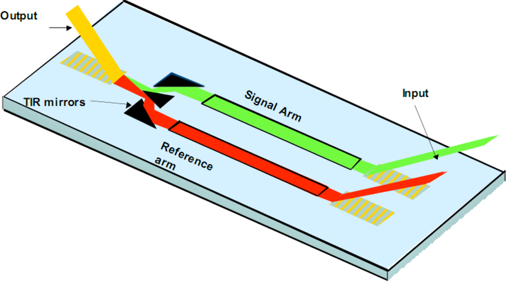
For discussion purposes, a interferometric sensor is illustrated in
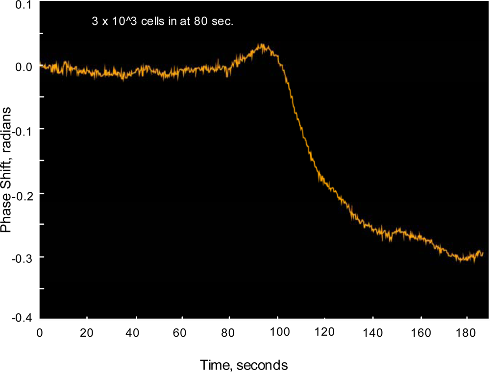
Figure 3. We have developed single and multi-channel (n = 4) variants of the same. Key IOC elements include grating couplers, the waveguide film with patterned sensing and reference arms, and a beam combiner. The interferometric sensor functions by directly detecting the selective binding of a biological agent onto a waveguide surface. The binding step causes a change in N
eff that is easily detected by interfering the guided wave traversing the signal arm of the interferometer with a guided wave traversing the reference arm. By monitoring the resulting interference pattern, any phase delay due to a change in the signal arm is easily detected. The phase delay is quantitatively related to the amount of biological agent bound to the waveguide surface and correspondingly the agent concentration in the sample solution undergoing testing. By treating the reference arm of the interferometer to look biologically similar to the signal arm, non-specific binding may also be minimized [
13]. Interferometric sensor systems have been used for chemical kinetic studies as well as detection of hazardous biological agents including toxins, bacteria and viruses.
3. Optical and Physical Principles of Waveguide-Based Detection
Planar waveguide sensing methodologies rely on the overlap of the evanescent field associated with a guided optical wave and the cover medium on or above the waveguide surface. This applies to both fluorescence and the interferometric sensing approaches. For fluorescence applications, the intensity of the guided wave excitation must be optimized at the boundary layer where capture of the biological target is concentrated, although the extent of the evanescent field must be restricted so as to limit fluorescence due to other materials present in the medium undergoing testing. Similarly, for interferometric sensing the evanescent electric field strength and overlap with bound biological species must be optimized to maximize the impact on the “effective refractive index” as seen by the guided optical wave. The optimization procedure is essentially the same for both sensing approaches and will be discussed based on the interferometric sensing concept.
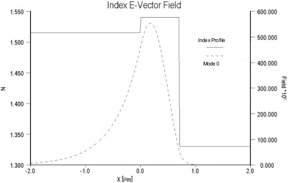
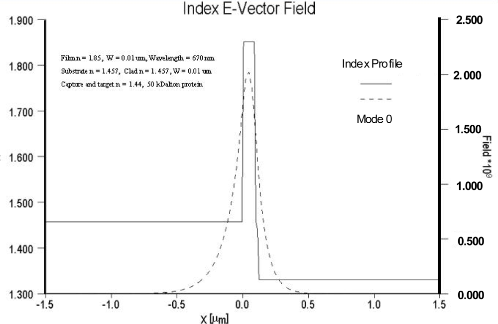
As noted previously, sensitivity is dependent on both the relative overlap of the evanescent field with the sensing layer as well as the electric field strength at the surface of the optical waveguide and sensing layer. For comparison purposes, the electric field distributions of two different waveguide systems are compared in
Figures 4 and
5. In
Figure 4 the field distribution is shown for a low contrast waveguide system typical of a glass substrate (n = 1.515) with a deposited waveguide film having a refractive index of 1.545 (Δn = 0.3) and a thickness of 0.62 μm.
Figure 5 depicts the field distribution of a high contrast waveguide system with a substrate index of 1.457 and film index of 1.85. For the high contrast waveguide system, the ratio of the area under the evanescent electric field within the cover medium relative to the total area under the electric field distribution curve is noticeably larger than that of the low contrast waveguide system. Equally important, the electric field strength at waveguide surface and cover medium interface of the high contrast waveguide system is more than an order of magnitude greater than that of the low contrast system.
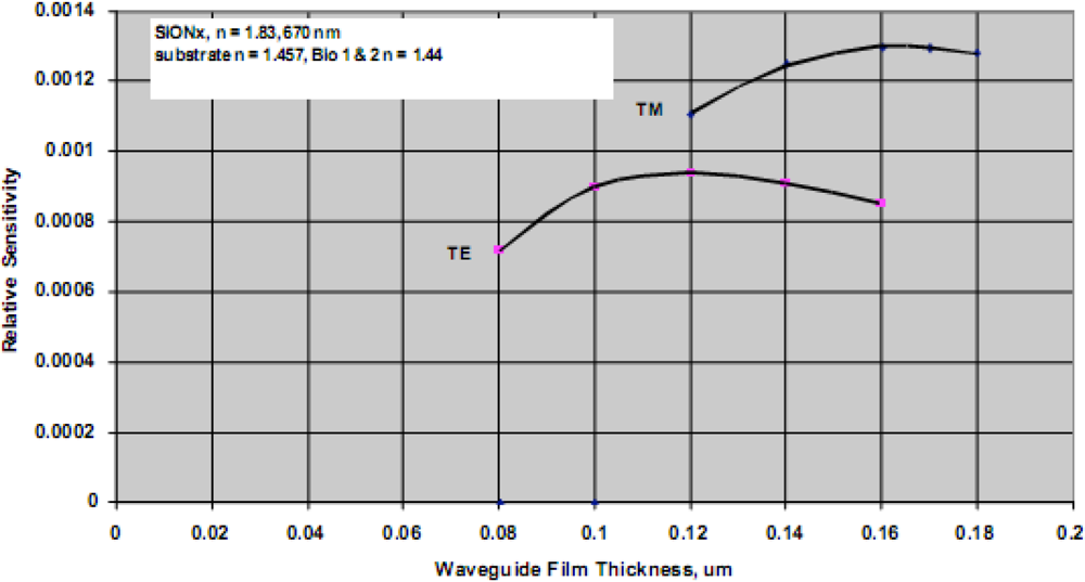
For a particular combination of waveguide material system, the film thickness providing maximum detection sensitivity for a biological agent can be predicted. The model used for this task assumes a waveguide with specific refractive index properties, operating at fixed optical wavelength, and a biological target with dimensions of approximately 5 nm and refractive index of 1.44 (typical for a 50 kDa protein). The analysis further assumes water as the cover medium over the waveguide surface. A typical result is shown in
Figure 6, indicating optimum detection sensitivity occurs at a film thickness of approximately 0.12 μm for a silicon oxynitride waveguide film on a fused silica substrate and TE polarization. For further comparison, the TM sensitivity is also shown, and as indicated previously is only slightly better than the predicted relative sensitivity for TE polarization. The inherent advantages of TE polarization more than makes up for the slightly enhanced detection limits associated with TM polarized light. To support guiding the low contrast waveguide film must be thicker, and as a result and the low contrast system is more than an order of magnitude less sensitive than that of the high contrast system. Going to material systems with increasing substrate/film index differences yields diminishing returns as the surface interaction begins to produce excess scattering losses. Ultimately substantial loss of the guided wave intensity occurs and cross-talk between closely spaced adjacent sensing results. This phenomenon also applies to reverse symmetry waveguides, which are waveguides with a substrate index that is lower than that of the bound biological agent.
4. Functionalization of Waveguides for Bioassays
The sensing film at the interface between the inorganic transducer and the media to be probed is critical in biosensing applications. The overall goal is amplified signal transduction triggered by a specific recognition event between the target analyte and the capture recognition ligand. To accomplish this, research teams have prepared a variety of films with the primary goals of: (1) suppressing non-specific binding of biological molecules to the transducer surface and (2) securely attaching, usually through covalent binding, a recognition ligand. Other attributes of the sensing film, such as fluidity to provide mobility of recognition ligands for binding to multivalent proteins [
14,
15] are also desirable. A variety of sensing films have been utilized for fluorescence-based detection on optical waveguides—phospholipid bilayers that provide fluidity, alkyl silanes with a distal reactive group (amines, thiols, epoxides, carboxylic acids, and aldehydes), polyethylene glycol chains, poly-amino acids, and proteins adsorbed to a surface. The emphasis researchers have placed on the attributes of sensing films depends greatly on the transducer used and, consequently, how non-specific signals are addressed (through surface functionalization or through instrumentation/reference channels). For the purpose of this review, we will mention several strategies that have been explored to provide a link between biological samples and transduction, with special emphasis placed on those strategies that address both the immobilization of a recognition ligand and the prevention of non-specific binding. We will not discuss ligand immobilization specifically; this topic has been reviewed in detail before [
13,
16,
17].
We have used supported phospholipids bilayers that contain low concentrations of small molecule receptors (e.g., GM-1) modified by the covalent conjugation of fluorescent dyes to detect cholera toxin [
14,
15]. Binding of multiple dye labeled GM-1 receptors to the cholera toxin brings the dyes into close proximity inducing fluorescence quenching or fluorescence resonant energy transfer. In addition to fluidity and the superior rejection of non-specific biding provided by phospholipids bilayers, multivalent biding results in enhance sensitivity by virtue of the surface avidity effect. More recently, we have used supported lipid bilayers as the sensing films for sandwich immunoassays as well.
Supported phospholipid bilayers are readily prepared on cleaned oxide surfaces by fusion of small bilayer vesicles [
18–
20]. Preparation of the vesicles and fusion to the surface can be accomplished in a relatively short period of time (4–6 hours) with readily available starting materials [
21,
22]. The resulting surface-bound bilayers can be used in sensing by attaching a capture element (such as biotin) or adding in a small amount of a functionalized lipid; the functional moiety is usually kept to a small percentage to minimize non-specific binding [
22]. Several antigens have been detected using these surfaces, including
Bacillus anthracis protective antigen (PA) [
22,
23], carcinoembryonic antigen (CEA) [
21,
24],
Mycobacterium tuberculosis lipoarabinomannan (LAM) [
25], and
Vibrio cholerae toxin [
14,
15,
26]. Despite the advantages of fluidity, rapid preparation and superb resistance to non-specific binding, as well as low auto-fluorescence at most useful wavelengths, phospholipid bilayers have notable disadvantages with respect to sandwich immunoassays. First, phospholipids only occur with limited functionality, the most useful being biotin. Assays that use phospholipids often rely on mobile ligands such as GM1 [
26], and must be chosen carefully to select capture agents that insert into lipid bilayers. The second major disadvantage of phospholipid bilayers is instability to some complex fluids (e.g., urine) [
27], detergent rinse, exposure to air, and extended periods of time in storage [
27–
29]. Chemical/terminal flexibility can be addressed synthetically [
30]; however, the preparative route necessary to create a molecule that can interact with lipid membranes and bulk solution while simultaneously incorporating a receptor and/or a fluorescent moiety is difficult. One strategy that we explored is the synthesis of a trifunctional linker moiety that contains lipid tails (acyl chains) for membrane anchoring, a fluorescent dyes and a functional group required for attachment of the recognition ligand [
30]. Stability has been addressed in a variety of ways, including chemically cross linking phospholipid bilayer [
29], coating the phospholipid with a streptavidin coating [
31], or capturing the bilayer in a sol-gel matrix [
32]. While promising, these stabilization methods remain unproven in actual biological assays on a waveguide platform; in the case of cross linking, defects appear that actually enhance non-specific binding [
29].
The use of poly- or oligoethylene glycol (PEG) chains has also been shown to reduce or eliminate non-specific binding of biomolecules to surfaces [
33–
38]. The main advantage of using PEG chains rather than phospholipid bilayers or other physically adsorbed polymers is the ability to conjugate them covalently to surfaces. This advantage has been demonstrated using PEG-terminated thiols on gold, and the parameters that affect the resistance of various PEG chain lengths, attachments, and terminations have also been investigated [
39]. Much of the work surrounding covalently attached PEG groups, however, has not been readily applicable to dielectric substrates, which are typically composed of oxides. There have been various solutions to this problem. Laibinis
et al. report an analogous silane that was prepared and used to coat the inner surface of a capillary for electrophoresis [
40,
41]. Desai and coworkers created PEG chains with terminal silanes and used these products directly to coat surfaces [
42,
43]. Kohler
et al. prepared bifunctional silane-PEG conjugates to coat magnetic particles for there cell targeting application [
44,
45]. Other researchers have attached PEG chains [
46–
48] or dextran groups [
49] to an amino acid backbone to effectively prevent non-specific binding. Only a few groups have prepared PEG films that simultaneously minimize non-specific interactions and maximize analyte binding for biosensing applications. For example, Zhen
et al. [
47–
49] have used PEG polymers (> 3.4 kDa) functionalized with lysine groups to cover surfaces for targeted sensing applications. However, these films lack covalent attachment to the surface, which makes them unusable when extended storage and reusability are required attributes. Thompson
et al. [
50] have overcome this issue by using a silane functionalized PEG polymer (MW > 3 kDa) that is covalently attached to an oxide surface for fluorescence-based bio-recognition experiments. Further, Seidel
et al. [
51] have used patterned amine functionalized PEG polymers, which are constructed on functionalized short chain silane monolayers, for multiplexed biosensing applications. Similar work by Majumdar
et al. used standard lithography techniques to prepare regions of functionalized silane monolayers for binding of analytes. These functional regions were surrounded by a field of PEG terminated silanes to prevent both non-specific binding to the background surface and reagent loss [
52].
In our laboratory, we have developed silane-based self-assembled monolayers (
Figure 7) that are very effective in minimization of non-specific interactions on waveguides during bioassays. For this, silica surfaces were functionalized by self-assembly of an amine-terminated silane film using both vapor- and solution-phase deposition of 3′-aminopropylmethyldiethoxysilane (APMDES). We found that vapor-phase deposition of APMDES under reduced pressure produced the highest quality monolayer films with uniform surface coverage, as determined by atomic force microscopy (AFM), ellipsometry, and contact angle measurements. The amine-terminated films were chemically modified with a mixture of carboxylic acid-terminated poly(ethylene glycol) (PEG) chains of varying functionality. A fraction of the PEG chains (0.1−10 mol%) terminated in biotin, which produced a surface with an affinity toward streptavidin. When used in sandwich immunoassays on waveguide platforms for the detection of several biomarkers such as the
Bacillus anthracis protective antigen, these functional PEG surfaces significantly reduced nonspecific binding to the waveguide surface while allowing for highly specific binding. A great advantage of SAMs was realized in the use of these surfaces for the detection of biomarkers in urine. As mentioned earlier, urinary salts destabilize lipid bilayers resulting in high non-specific binding. However, we have been able to use SAM-functionalized waveguides for detection of urinary biomarkers with no increase in non-specific binding [
27,
28]. We have also successfully detected
Mycobacterium tuberculosis virulence factors in patient urine using SAM functionalized waveguides [
30]. We have found these silane-based self-assembled monolayers (SAMs) to be robust (stable for > 300 days in air), resistant to non-specific binding even with high-salt samples such as urine, resistant to washing with potent solvents, buffers and detergents and potentially reusable. The lack of fluidity of SAM surfaces precludes their use with fluroescence resonance energy transfer assays and other techniques that require mobility of the biomolecules involved. We have used planar optical waveguides functionalized with SAMs for many of our biodetection assays with excellent results (Section 6).
Two basic methods exist for preparing covalently attached PEG-terminated thin films: deposition of molecules synthesized using
de novo preparative routes to form a self-assembled monolayer of that synthetic molecule [
40–
44], or stepwise functionalization of a simpler self-assembled mono-layer [
27,
53]. Either method is adequate for prevention of non-specific binding; however, if a biological molecule or receptor will be attached to the surface, one must weigh the pros and cons of each method. Deposition of complete molecules leads to a more efficient coating process and less ‘down time’ between assays, but requires synthetic effort to create the necessary silanes (at least two are required—one for prevention of non-specific binding (NSB), and one for ligand attachment); a “build up” method of sequential depositions and reactions on a surface slows the coating process but eliminates the synthesis. The “build up” method also requires at least two PEG reagents, but the synthetic effort required is usually reduced because many bifunctional PEG reagents are available commercially from sources such as Fluka
™, QuantaBiodesign
™, and Nektar
™.
6. The Los Alamos Waveguide-based Optical Biosensor
Our team has developed a waveguide-based biosensor that we have successfully adapted to the detection of biomarkers in complex biological samples. Historically, we have evaluated both sol gel and SiON
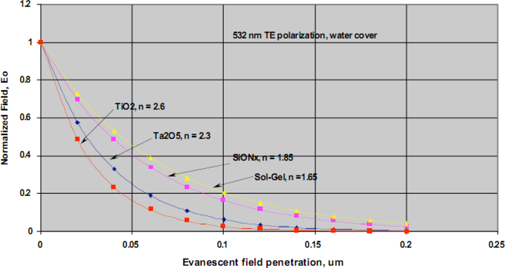
x waveguide materials for our sensor platform. The normalized evanescent field decay for different waveguide materials is shown in
Figure 10. As indicated, there is a rapid decay in evanescent field intensity and light does not penetrate the sample beyond ∼200 nm. This spatial filtering is a distinct advantage of all evanescent wave-based detection platforms as it ensures that the bulk biological sample is not irradiated. This arrangement effectively minimizes background fluorescence and eliminates the need for extensive sample preparation when analyzing complex samples. Another critical advantage of evanescent field detection is the intense field strength at the surface where the detection occurs, facilitating observation of very low concentrations of our fluorescence reporters [
22,
55].
Much of the early work with optical waveguides in our laboratory utilized fluorescence resonance energy transfer triggered by the binding event between multivalent protein and dye-tagged receptors [
14,
15,
64]. Sensitive detection of the cholera toxin was achieved by facilitating the binding of the toxin to its receptor (GM1) on a fluid lipid bilayer coated over waveguide surface. The toxin-binding event brought up to five GM1 and their reporter dyes conjugated to them in close proximity thereby inducing self-quenching or fluorescence resonant energy transfer and facilitating toxin detection at picomolar concentrations. Subsequently, we developed both a laboratory test-bed system and a hand-held detector for the detection of biomarkers [
26]. The portable test-bed system (
Figure 11) has been extensively described [
21] and has been subsequently used for the detection of biomarkers associated with several diseases in a sandwich immunoassay format [
21,
23,
24]. This system uses either a stabilized 532 nm diode pumped laser or a 635 nm diode laser for excitation, depending on the excitation wavelength of the fluorescent reporter in the assay. Grating couplers provide a facile method to couple excitation light into the thin waveguide material. Laser light is coupled into the waveguide by positioning the excitation beam onto the diffraction grating at the appropriate angle of impingement. The angle is determined by the effective mode index of the waveguiding film, film thickness, and the period and amplitude of the grating structure. These parameters are adjusted to provide a 10°–15° input coupling angle for an excitation wavelength of 532 nm. A USB 2000 fiber optic Spectrometer interface (Ocean Optics Inc. FL, USA), positioned normal to the waveguide surface to collect isotropic emissions. A long pass filter, one that does not affect transmission of light at longer wavelengths, is used to remove excitation light form the resulting fluorescence spectra. All optical components are mounted on an optical bench. A PC interface is available for monitoring and controlling of experimental parameters and to record data.
Fluorescence resonance energy transfer assays, as described above, cannot be adapted to all biomolecules with excellent sensitivity and require a significant investment in ligand development. Therefore, we have concentrated on fluorescence-based sandwich immunoassays on the planar waveguide surface. We have used both phospholipid bilayers [
21,
23] and self-assembled monolayers (SAMs) [
27,
28] for waveguide functionalization, and the relative advantages and disadvantages of these techniques were discussed earlier (Section 4). Functionalized waveguides are mounted on a specially designed flow cell. A schematic representation of a fluorescence-based sandwich immunoassay on a functionalized waveguide is indicated in
Figure 7 and has been described in detail before [
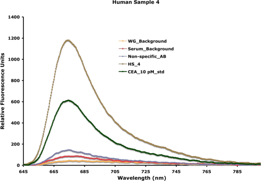
24]. We have used this approach to detect extremely low concentrations of disease biomarkers in actual patient samples. A typical detection spectra obtained from the experimental measurement of carcinoembryonic antigen, a breast cancer biomarker, patient serum samples is indicated in
Figure 12.
In all experiments, the waveguide-associated background, an intrinsic measure of impurities associated with the waveguide itself, is measured, and used as the background for data extrapolation. NSB associated with control complex samples (e.g., control serum) and the fluorescently labeled reporter antibody is measured in each experiment. As indicated in
Figure 12, background fluorescence from NSB is very low, because of the detection within the evanescent field and the resistance of the functional surface (SAMs) to NSB (discussed earlier in Section 4). A capture antibody is entrapped in the surface based on biotin-avidin chemistry. Addition of the sample facilitates the binding of the antigen, when present, to the capture antibody. Addition of the reporter antibody allows for specific fluorescence measurement associated with antigen-antibody interaction. Using two antibodies, in a sandwich format, for antigen detection offers additional specificity of detection. In the detection of unknown patient samples, an internal known standard is measured first, facilitating the extrapolation of concentration of the antigen of interest in the sample. We have used this approach to detect and quantify carcinoembryonic antigen in serum and nipple aspirate fluid from patients with abnormal mammograms [
24] and obtained 100% corroboration with disease progression in a blind study. The limit of detection of our assay is 500 femtomolar (< 1 ng/mL), which is lower than that achieved by traditional plate-based assay formats. Similarly, we have been able to detect
Mycobacterium tuberculosis specific virulence factors in urine from infected patients, also in a blind study [
25]. Our team has also synthesized carbohydrate ligands for the discriminatory detection of influenza viruses using a convergent strategy and demonstrated the detection of intact viruses on our waveguide-based platform [
61]. More recently, we have successfully conjugated antibodies with QDs and used them in a multiplex detection assay for
Bacillus anthracis lethal factor and protective antigen. We were able to detect these antigens with much better sensitivity than attained by conventional plate-based immunoassays using the same antibodies [
21–
25,
65(unpublished data)].

