1. Introduction
Voltage source inverters are a key component in most PV systems installed for grid connected and standalone applications [
1,
2,
3,
4]. These inverters use sinusoidal Pulse Width Modulation (PWM) strategy which involves high speed switching of semiconductor devices to produce an AC output which generates high frequency noise, harmonics and cause high switching losses. A passive filter, which is cost effective, is connected between the inverter and the grid to attenuate the PWM carrier and sideband harmonics to meet IEEE standards. Earlier, first order passive L type filters were used on the AC side of the PWM inverters for attenuation of these switching harmonics. However, L filter has a restriction in low switching frequency applications due to its inevitable large size [
5,
6]. A higher order LC or LCL filter provides better harmonic suppression at lower switching frequencies with a reduction of overall filter size. The LCL filter instead of L filter is more attractive because it can provide high frequency harmonic attenuation with the same inductance value [
7,
8,
9]. Conversely, these higher order filters trigger a resonance between the inverter and the grid which needs to be damped either actively [
10,
11] or passively [
12,
13,
14,
15,
16,
17,
18,
19,
20,
21,
22,
23,
24]. Active damping methods being flexible, involve a well-designed control algorithm to dampen the resonance but are limited by high cost, control complexity and the use of additional sensors. Passive damping schemes are economical, less complex and carry an increased reliability.
Various filter topologies and damping techniques for passive filters have been proposed in the literature for voltage source inverters. Different damping schemes for a passive filter used in grid connected inverters is discussed [
9,
12,
13]. However, the procedure to design the filter parameters and the damping component is not provided. A structured procedural analysis and comparison of active and passive damping methods for LCL filters employed in a grid connected voltage source converter is explained in [
14]. However, the analysis described in the paper is specific to low power applications operating at high switching frequencies. Passive LCL filters with a resistance connected across the filter inductor on the grid side have been more popular for three phase grid connected inverter systems working at a particular resonant and switching frequency [
15,
16]. In [
15], the resistance value is chosen approximately from bode plots obtained for a set of resistance values selected using trial-and-error method, whereas plots are presented for the loss obtained in the inverter and filter system and compared with the loss obtained using active damping technique in [
16]. Neither of them provide information on the selection of optimal damping components [
15,
16]. In [
8], the value of the damping resistance in a LCL filter used in a three phase rectifier system is assumed to be one-third of the LCL filter capacitor impedance at resonant frequency. Although the performance of the filter is proven to be efficient, the selection procedure may not be suitable for all conditions. Another design approach where a virtual resistor is assumed to be on the output side of the LC filter side to damp the switching oscillations in a PWM inverter is proposed in [
17]. On the other hand, an extra control algorithm that simulates the role of a real resistor makes the system complex. To overcome this, a method that uses a resistor to help dissipate the energy stored in the resonant circuit of a LC filter used in an IGBT inverter is proposed for motor drive applications [
18]. However, the above filter is designed with a resonant frequency above the switching frequency, since the purpose is to limit merely dv/dt and not to suppress the switching harmonics. Another design method where a resistor is connected in series with the filter inductor to damp harmonic resonance at the DC link of a rectifier-inverter system is proposed in [
19]. A detailed analysis of a split-capacitor with resistive (SC-R) damping for a LCL filter used in a three-phase grid connected inverter that includes power loss in the damping resistance in the analysis is done in [
20]. A design-oriented analysis for the selection of the split-capacitor resistive (SC-R) damping circuit parameters is presented in [
6]. Since the capacitor in the damping branch is split from the filtering capacitor in [
6,
20], the high-frequency harmonic attenuation of the passively damped LCL filter is reduced, compared to that with an undamped LCL filter. Another simple design criterion to find the optimized damping resistor values used in a LCL and a higher order LLCL filter is proposed in [
21]. In the above work, an additional RC branch in connected across the trap filter to perform passive damping. However, LLCL filter provides a lesser harmonic attenuation performance in the high frequency band [
22]. To overcome this, a new high-order filter, named the LTCL filter, is proposed in [
23] with multiple LC traps inserted in parallel with the capacitor branch. However, multiple traps tuned to different frequencies require judiciously selected components to attain desired harmonic attenuation. Another novel passive filter, namely, L(LCL)
2, is employed for a grid inverter in [
24], where a design bench mark is utilized to obtain the filter component values and the inductance present in the filter design is optimized using Genetic algorithm. Although optimization techniques such as Particle Swarm Optimization (PSO) and Genetic Algorithms have been utilized to obtain filtering component values in LCL filters employed in rectifiers, and power filters [
24,
25,
26], these algorithms work based on allowable components value ranges for choosing the reactive elements in the filter. Poor design of output filters leads to reduced attenuation at the switching frequency, larger filter size, higher cost and more losses. Hence, it becomes a challenging task to design the filter components with reduced size, good damping and improved attenuation.
Recently, multilevel inverters are more researched due to the advantages they offer over conventional voltage source inverters in grid connected applications [
27,
28,
29]. Among the different multilevel inverter topologies [
30], Cascaded H-Bridge (CHB) inverters [
31] are advantageous owing to their modularity, simplicity and they require fewer components to achieve the same number of voltage levels. Although there are various modulation techniques [
30] available for multilevel inverters, modulation based on multi carrier signal arrangements with traditional sinusoidal PWM technique such as Phase Disposition PWM (PDPWM), Phase Opposition Disposition PWM (PODPWM) and Alternative Phase Opposition Disposition PWM (APODPWM) [
32,
33] are quite popular and simple to implement, which again necessitates a filter at the inverter output to limit the harmonics caused by PWM. Several methods based on the basic modulation techniques have been used for minimization of harmonics in multilevel inverters [
34,
35,
36,
37]. However, all these methods involve a well-designed modulation scheme and involve a complicated power circuit design to obtain better quality. Instead, passive filters are economical and simple to improve power quality. Passive filter designs considering LC trap/LCR filter and LCL filters for a neutral point clamped three level inverter is presented in literature [
38,
39]. The analysis and performance of a LCL filter for a cascaded inverter operating as a DSTATCOM is studied in [
40]. However, the analysis is restricted to low frequency operation in [
38] and [
40]. Most of the literature has focused on filter designs for conventional voltage source inverters and filter designs considering multilevel inverters is limited. To address the above challenges, this work proposes a new L-(CR)
2-L passive filter structure for a pulse width modulated inverter used in grid connected applications. The design consists of an additional resistance–capacitance branch across the filter capacitor of the traditional LCL filter apart from an additional resistance in series with the filter capacitor. The proposed filter can attenuate the switching frequency harmonics much better than the traditional LCL filter, while maintaining the same overall inductance value and reduced capacitance value of the traditional LCL filter. It can reduce the damping power loss with lesser value of damping resistance and provides considerable damping power loss reduction compared to conventional topologies. Further, this work includes the basic parameter design procedure with expressions to arrive at individual filter component values of the proposed filter in addition to a novel technique using PSO to minimize damping power loss, while ensuring reduced resonant peaking. Further, the same algorithm is also employed to ensure maximize harmonic attenuation in and around the switching frequency based on permissible filter inductance and capacitance values. A performance comparison of the proposed filter against two other passive filters is presented. Results obtained from experiments conducted on a 1 kW, 110 V, 50 Hz five-level inverter set up based on a SPARTAN 6-XC6SLX25 Field Programmable Gate Array (FPGA) processor are included to evaluate the performance of the proposed filter. This work considers a five-level CHB inverter for the filter implementation. The structure of a five-level CHB inverter interfaced with the grid through a traditional LCL filter is presented in
Figure 1. In
Figure 1,
Vs1 and
Vs2 represents the DC voltage applied to the upper and lower H-bridges of the five-level inverter,
S1 to
S8 are the inverter switches,
Linv and
Lgrid represents the inverter side and grid side inductance of the LCL filter respectively and
C represents the LCL filter capacitance. PDPWM modulation technique [
33], which is well discussed in the literature, is used to generate gate signals for the five-level inverter.
The rest of the paper is organized as follows:
Section 2 provides the complete analysis and design of the proposed passive filter structure.
Section 3 focuses on the filter parameter design and verification. Simulation and experimental results are provided in
Section 4. The work is concluded in
Section 5.
2. Proposed Filter Design
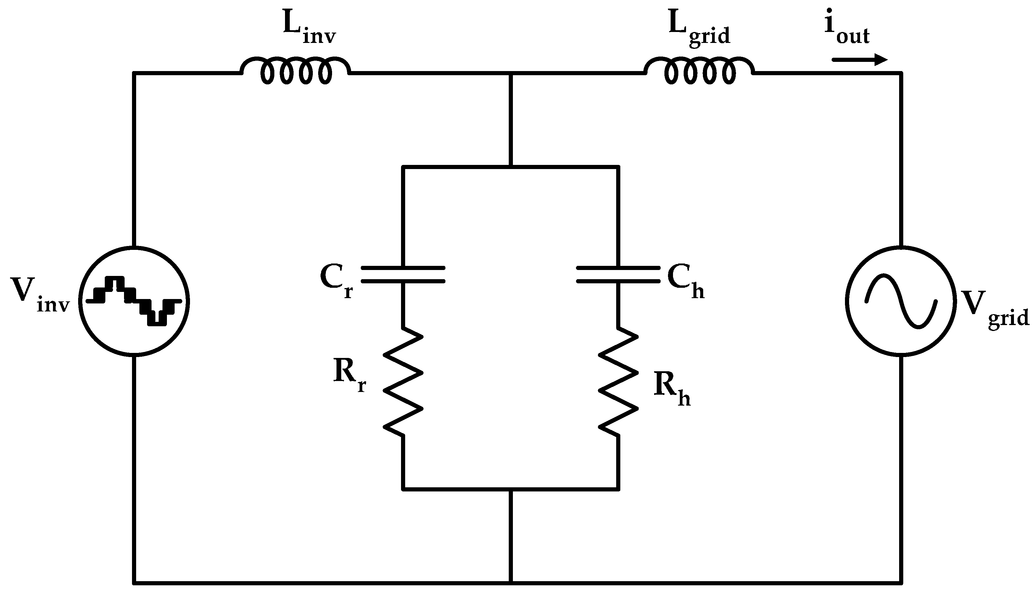
The proposed filter is presented in
Figure 2. In
Figure 2,
Linv represents the inverter side inductance,
Lgrid is the grid side inductance and
Cr is the filter capacitance.
Rr is the series resistance to damp resonance.
Rh-
Ch represents the additional R-C branch connected across the
Rr-
Cr branch mainly to bypass harmonic components and to reduce damping power loss.
iout represents the grid side current.
The transfer function of the proposed filter structure is derived as in Equation (1).
2.1. Selection of Overall Inductor and Capacitor Values for the Proposed Filter
Larger values of capacitance for the proposed configuration provide better higher order harmonic attenuation. However, it results in higher reactive power and increased demand of current from the inverter side inductance, resulting in the decrease of efficiency of the overall filter system. In addition, smaller capacitor size requires larger inductance to meet the harmonic mitigation requirement. Thus, the selection of capacitor value for the proposed filter is a tradeoff between the reactive power and the selection of inductor values. The overall capacitance value (
) for the proposed filter configuration is chosen by calculating the reactive power absorbed by the filter at rated conditions as given by Equation (2).
where
Q is the reactive power absorbed by the system, which is usually chosen to be less than 5% of the rated power [
21,
23];
Vgrid is the rated system voltage; and
fout is the output frequency of the system.
A number of methods have been used in the literature to select inductor values in a LCL filter [
6,
9,
12,
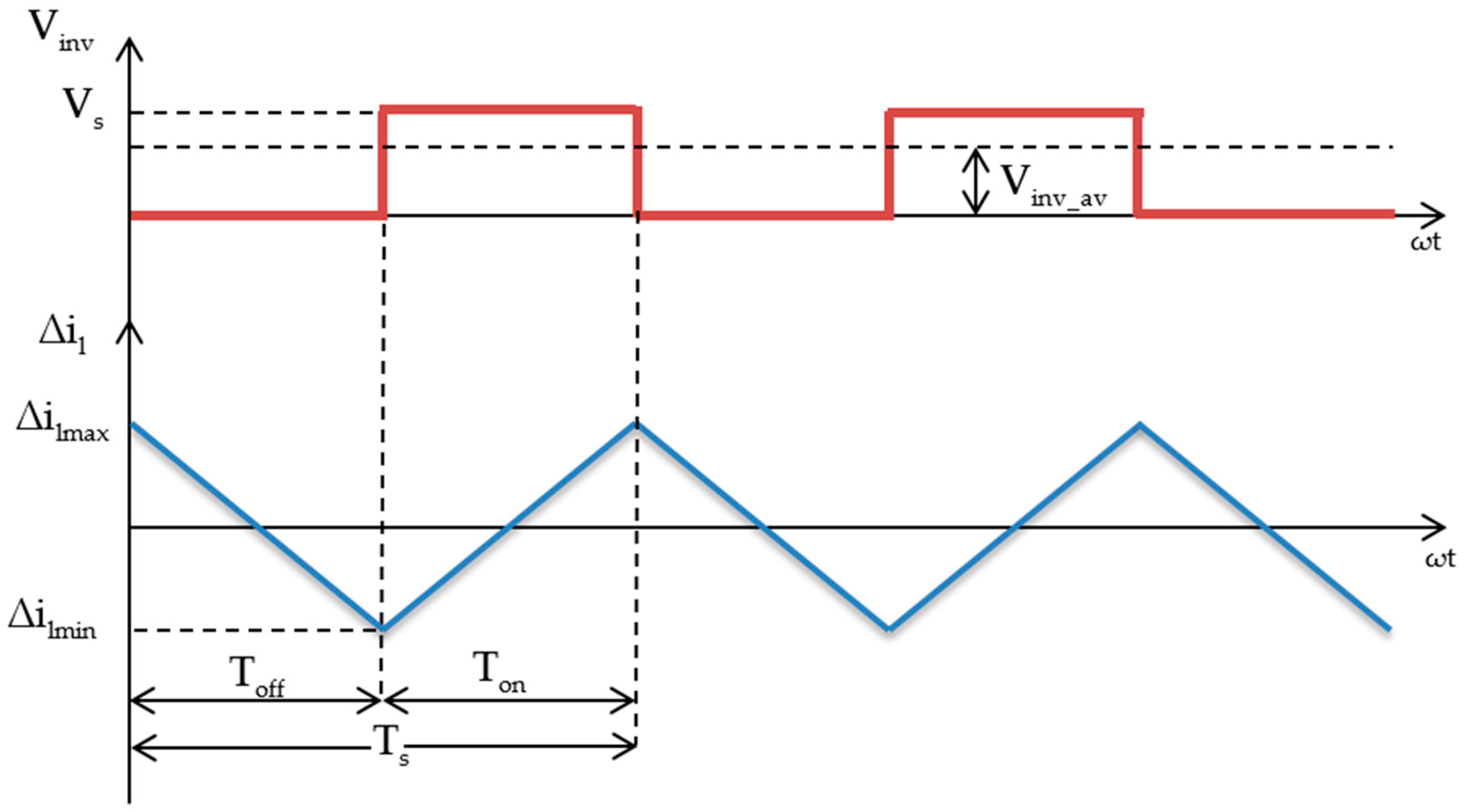
20]. This work considers some of those aspects to design suitable inductor values for the proposed structure. The inverter side inductance is usually designed by calculating the current ripple. Selection of small values of ripple current decreases the switching losses. However, it results in large values of inductors. Thus, the selection of the ripple current is a trade-off between the size of the inductors and the switching losses. The inverter output voltage and inductor current waveforms during one switching cycle for a carrier based modulation is shown in
Figure 3.
The inverter switching frequency is usually greater than the system output frequency. Hence, the average value of the inverter output voltage can be treated constant during the switching period
Ts. In
Figure 3,
Vinv_av represents the average inverter output voltage, while
Ton and
Toff represent the ON and OFF periods. The turn ON and OFF times are related as
Toff/Ton = 1
− α and
Ton/Ts = α, where α represents the duty cycle. The peak-to-peak value of the inductor current during PWM switching is obtained using Equation (3) [
24].
where
Linv represents the inverter side inductance of the passive filter and
Vs (
Vs1 = Vs2 = Vs) is the voltage applied to one of the H-Bridges of the inverter. As the grid voltage is usually assumed to be purely sinusoidal, the fundamental component of the grid current can be assumed to be zero. Hence, the fundamental component of voltage appearing across the inductor is zero. Hence, the inverter average output voltage and grid voltage are given as
and
where
m is the modulation index. Using the above expressions, Equation (3) is rewritten as Equation (4).
Equation (4) provides the peak-to-peak value of the inductor ripple current. Thus, inverter side inductance value
Linv of the proposed filter is using Equation (5).
where
Vs is the input voltage to one H-Bridge of the inverter, “
h” is the amount of ripple current which is generally lower than 40% of the peak value of the rated system current [
21,
22] and
fswitch is the switching frequency of the inverter.
The value of grid side inductance,
Lgrid is chosen such that
Lgrid = a Linv, where “
a” is the inductance ratio factor. With the factor “
a” less than unity (
Lgrid < Linv), it is possible to reduce the overrating of the switches and improve stability. This design approach is used for grid side inductor design in [
12,
23]. With the factor chosen as unity, the inverter and grid side inductances are made equal to maximize the attenuation capability of the LCL filter [
21,
22]. However, this results in an increased cost and volume of the filter elements. Choosing
a > 1 results in a smaller inverter side inductance [
14] when compared to the grid side. This design may introduce significant current ripples on the inverter output leading to serious overheating and losses on the inductor [
5]. It also increases the ratings of the switches raising the cost and switching losses. Considering another criterion, the overall inductance value of the proposed filter is to be kept less than 0.1 per unit to limit the voltage drop across the inductor [
20].
2.2. Selection of Resonant Frequency
A good selection of the resonant frequency is another important design criterion considered for the design of the proposed filter. The resonant frequency is usually chosen based on the fundamental frequency and switching frequency of the inverter. It is chosen such that it is in the range 10
fout ≤ fres ≤ (
fswitch/2) to ensure that resonant and switching harmonic currents flow through the respective branches of the filter circuit. The resonant frequency of the proposed filter is given by Equation (6).
2.3. Selection of Individual Filter Components
The
Rh-
Ch branch in the proposed filter is designed to provide a path for the current harmonics at and around the switching frequency,
ω = ωswitch, as given by Equation (7).
where
is the impedance offered by the
Rh-
Ch branch at the switching frequency and
is the impedance of the
Rr-
Cr branch at the switching frequency. The
Rr-
Cr branch is designed to provide a path for the current around the resonant frequency,
ω = ωres as given by Equation (8).
where
and
are the impedances offered by the
Rr-
Cr and
Rh-
Ch branches at resonant frequency. A careful design is required for the proper choice of
Rr-
Cr and
Rh-
Ch branch values. Equal capacitor values are considered for both the branches in [
20]. Further, the overall capacitance of the filter circuit should also meet the reactive power absorption of lesser than 5% as given in Equation (2). Choice of equal capacitor values for the proposed structure may not offer the required impedances at the resonant and switching frequencies. Hence, as per Equations (7) and (8), a new factor called capacitance ratio is introduced, which is given by
Cr/Ch with
Ch less than the
Cr branch value. From the knowledge of the switching frequency and the resonant frequency, which is usually near to half of the switching frequency value, the design of
Ch and
Cr is carried out. The values of
Rr and
Rh are required to compute the impedance offered by the two parallel branches which influences the harmonic and resonant current flow path and subsequently the losses.
Again, the selection of
Rr and
Rh requires careful steps to follow Equations (7) and (8). The impedance of the
Rr-
Cr and
Rh-
Ch circuit branch is calculated and given by Equation (9).
The resistance
Rr can vary between zero and infinity ohms. Therefore, the impedance is limited within the range given by Equation (10).
For a minimum value of
Rh, accordingly, for a good damping effect, the resonant frequency should fall in the range calculated and given by Equation (11).
Equation (11) is rewritten as Equation (12) which is useful to fix the range of
Rr.
where
ωres = 2
πfres and
fres is given by Equation (6). For a minimum value of
Rh, as
Rr varies between zero ohms and infinity ohms, the resonant frequency varies between a minimum value and maximum value as given by Equation (13).
From Equations (12) and (13), the value of Rr can be fixed. For lower values of resonant frequency, higher damping resistance value is obtained and vice versa.
The resistance
Rh can vary between zero ohms and infinity ohms. Therefore, the impedance of the parallel filter branch is limited within values given by Equations (14) and (15).
The aim of
RhCh branch is to provide path for high frequency harmonics. Further, the value of
Rh should be lesser and simultaneously minimize damping loss with reduced
Rr. Thus, for minimum
Rh, based on impedance offered, the switching frequency is limited within the range given using Equation (16).
Introducing resistance ratio factor as
Combining Equations (16) and (17), the selection of R
h falls within the range as given by Equation (18).
where the value of resistance ratio factor is less than unity to minimize damping loss. The next section discusses the effect of resistance ratio factor on damping power loss.
Since the aim of Rh-Ch branch is to pass on the maximum switching ripple components through it, the value of Rh is chosen to be smaller than Rr to provide the necessary lesser impedance at the switching frequency as Ch < Cr. Now, with two parallel branches, Rr-Cr and Rh-Ch, the current through Rr and Rh varies based on their impedance. In the proposed damping scheme, the switching harmonic currents largely pass through the Rh-Ch branch and the resonant current flows predominantly through the Rr-Cr branch. The Rh-Ch branch, with a lesser resistance and capacitance value provides an alternate non dissipative path (with a smaller resistance which also improves harmonic attenuation, the loss in the resistance is almost negligible) for the high frequency currents thereby reducing the harmonic damping losses. The Rr-Cr branch, with a higher resistance and a slightly high capacitance value than the Rh-Ch branch (In this branch, the resistance value required becomes small when compared to traditional Rd-Cd damping) provides an alternate path for the resonance currents thereby reducing the losses in the damping circuitry.
2.4. Damping Power Loss
The power dissipated in the Rr-Cr and Rh-Ch circuit is calculated separately at the fundamental and switching frequencies.
- (i)
Fundamental frequency: The power loss at fundamental frequency is given in Equation (19).
where
ωout is the fundamental frequency in rad/s. Further, with two parallel branches
Cr and
Ch, the resulting current through
Rr is halved, thereby reducing the damping loss at fundamental frequency.
- (ii)
Switching frequency: The power loss at switching frequency is given by Equation (20).
where
Idamp is the current through the damping branch comprising of parallel combination of
Rr,
Cr and
Rh,
Ch and is given by Equation (21).
where
Zdamp is calculated from Equation (9) at switching frequency.
The voltage across the damping branch
Vdamp is given by Equation (22).
where
VAM gives the harmonic amplitudes of the five-level inverter output voltage given by [
33] and
YdampM (at
) is given by Equation (23)
and given as
where
Z1 and
Z2 are the impedances offered by
Linv and
Lgrid, respectively.
- (iii)
Total Power Loss
The total power loss in the damping circuit is given the sum of the fundamental frequency power loss and the switching frequency power loss as Equation (25).
2.5. Optimization to Maximize Harmonic Attenuation using PSO
Frequent trial and error in a design procedure increases the need to optimize parameters. PSO is a stochastic optimization algorithm based on deterministic points of natural selection that simulate the natural process of group communication of a swarm of animals when they flock or hunt with a velocity. If one member finds a desired path, the rest of the swarm will follow it. The PSO algorithm imitates the behavior of such animals by particles with an initial velocity and position in space. With a random population (called swarm), each particle (member of swarm) flies through the search space and remembers the best position [
25]. The members communicate among themselves these positions and adjust their own position and velocity in a dynamic fashion. This way the particles fly towards an optimum position. In passive filter designs, it is challenging to achieve maximum harmonic attenuation while selecting the filter components judiciously within their allowable limits. The selection of filter components affects the design performance index such as THD, size, harmonic attenuation ratio, etc. To maximize attenuation around the switching frequency and its multiples, PSO algorithm is employed in this work. The target of optimization is to obtain maximum value of harmonic attenuation considering the values of the filter inductance and capacitance. The objective function to obtain maximum harmonic attenuation for the proposed filter is expressed as Equation (26).
where
G(jω) is given by is given by
Subject to
- (i)
Lmin < Linv < Lmax, where Lmin and Lmax are the minimum and maximum allowable inverter side inductance values, respectively.
- (ii)
Cmin < Ct < Cmax, where Cmin and Cmax are the minimum and maximum allowable capacitance values, respectively.
The relation between inverter side and grid side inductances and maximum/minimum value of inductance and capacitance is presented in
Section 2.1.
- (iii)
Harmonics greater than 35 should be less than <0.3% of the rated fundamental current as per IEEE 519-1992 standards. The current harmonic attenuation is computed by considering that, at high frequencies, the converter is a harmonic generator, while the grid is considered as short circuit source. The magnitude of switching ripple current to inverter voltage ripple at the switching frequency is evaluated using Equation (27).
The magnitude of the switching ripple current at the switching frequency is guided by the recommendations of IEEE 519-1992 (harmonic magnitude to be lesser than 0.3% of fundamental). With inverter side inductance values of 1 mH, 2 mH and 3 mH computed as discussed in
Section 2.1, the maximum magnitude of harmonics greater than 35 (since harmonics are mostly around switching frequency, the magnitude is evaluated at 10 kHz) is found to be 0.37%, 0.16% and 0.28% of rated fundamental current, respectively. Hence, the inverter inductance is chosen as 2 mH. Compared to step-by-step method, this value has 1% error.
2.6. Optimization to Minimize Damping Power Loss Using PSO
Reactive components used in passive filters inherently produce switching oscillations that needs to be damped. These oscillations appear as a peak amplitude at the resonant frequency. The damping resistance used to suppress these oscillations produces power loss and weakens the high frequency attenuation ability. To efficiently use the damping circuit in the proposed design, this work considers the damping power loss, damping resistance value and the damping of resonant oscillations. In the proposed work, care is taken that the damping resistance does not weaken the harmonic attenuation and does not contribute to damping power loss. The damped filter should show more attenuation at the resonant frequency as well as in the high frequency band. This work uses PSO algorithm to minimize power loss on the premise of allowable damping resistance value and minimum peaking in the resonance. An objective function is defined that minimizes the power loss. In the following section, the steps towards an optimal design to minimize damping power loss is described:
Particle: The particle of particle swarm optimization is denoted by a set of two-dimensional vector as .
Objective Function: This paper uses Equation (28) as the objective function that minimizes the damping power loss.
where
Ptotal is defined from Equation (25) that includes fundamental and switching frequency power loss given by Equations (23) and (24).
Subject to the Constraints:
- (a)
The harmonics produced due to PWM is mainly located at the switching frequency and its multiples. The frequency response characteristics of the proposed filter shows that the filter produces attenuation with a slope of 60 dB/decade after the resonant frequency. Therefore, if the switching frequency is located far from the resonant frequency, the greater the attenuation at the switching frequency would be. The amplitude function of the grid current to the inverter voltage at the switching frequency is given using Equation (29).
- (b)
The shunt damping resistance is limited as
, where
Rd = Rr + Rh and
Rdmin and
Rdmax are the minimum and maximum allowable values of the shunt damping resistance (sum of
Rr and
Rh) value, respectively, as discussed in
Section 2.2.
The search process begins with the initialization of the particles, number of populations, generations, best values of the objective function in the local search and global search [
28]. The defined objective function is calculated for various values of resistance and is stored as an array. If the constraints are satisfied, a comparison is established between the obtained objective function value and the best value that is searched by the particles and is stored as
Pbest. A comparison is also made with the global best value that is searched by all the particles and stored as
Gbest. The search is repeated until all the populations and generations are exhausted. The PSO algorithm renews the position and velocity to search the whole space by
where “
V” is the velocity of the particle, Present is the present position of the particle, P
best and G
best represents the partial optimal solution and global optimal solution.
λ is weighted factor ranging from 0.1 to 0.9.
α1 and
α2 are the learning factors, commonly taken as a value equal to two [
25].
3. Parameter Design, Verification and Discussion
With above design and constraints considered, the proposed filter configuration is constructed for a five-level inverter.
Table 1 depicts the system parameters.
Table 2 shows the designed filter component values. To assess the performance of the proposed filter, two filters namely LCL filter with resistance damping [
21,
22] (Filter I), and
Rd-
Cd damped LCL filter [
20,
21] (Filter II) are compared with the proposed filter (Filter III). The overall inductance and capacitance values of all filters (for Filter III, capacitance becomes lesser as per design) are maintained the same. The damping circuit parameters of Filter I and Filter II are based on [
21] and are listed in
Table 2.
The frequency response characteristics obtained for the three filters based on the above design parameters is depicted in
Figure 4. It is clear that the proposed filter provides greater attenuating effect on the harmonics when compared to the
Rd-
Cd damped LCL filter. The proposed filter exhibits high harmonic attenuation capability in the high frequency band while maintaining the same overall inductance and capacitance values compared to Filter I and Filter II.
From Equation (25), it is clear that changes in inverter switching frequency changes the damping power loss. If switching frequency varies, the parameters of the filters also vary. High switching frequency operation necessitates lesser values of filter components.
Figure 5 presents the damping loss achieved with all the three filters for different values of switching frequency. It is seen that Filter III provides reduced damping loss compared to Filter I and Filter II at the switching frequencies considered because the impedance of the
Rh-
Ch branch is less at the switching frequency, providing a bypass path for high frequency harmonic currents as per the proposed design.
Figure 6 presents the damping loss achieved with all three filters for different values of modulation index. With the proposed filter, lower damping power loss is obtained compared to the other two filters at all of the modulation indices considered, as the majority of the high frequency harmonic currents circulate through the
Rh-
Ch branch, bypassing the
Rr branch.
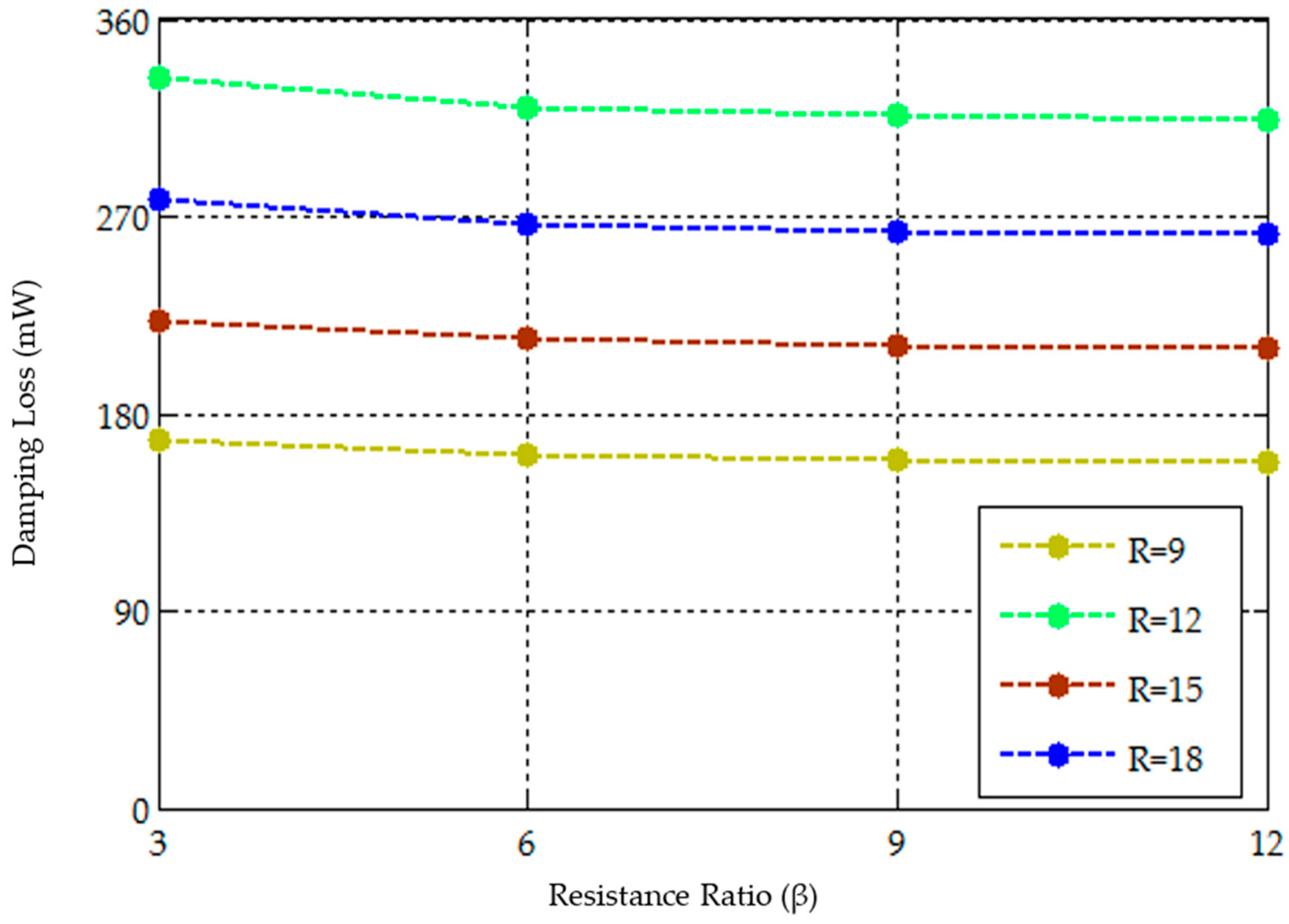
Figure 7 presents the damping loss variation achieved for variation in the values of the resistance ratio by keeping
Rr constant. It is seen in
Figure 7 that, at higher values of
β, the damping power loss is reduced for any value of
Rr. Again, for a particular
β, as the value of
Rr increases, the damping losses increase. This is expected, as increase in the resistance value increases the damping power loss. Thus, to reduce the damping power loss, lower values of
Rr is chosen and, at the same time, higher value of resistance loss ratio is chosen. Choosing a higher resistance ratio factor helps in choosing lower values of
Rr in the proposed design. Hence, the resistance parameter selection for both the parallel branch circuits of the proposed filter plays a vital role in reducing the overall damping losses. The curves validate the design value selection of the resistances used in the proposed filter design.
Figure 8 and
Figure 9 present the variation of damping loss and harmonics (maximum harmonic magnitude with respect to fundamental) achieved for different values of
Cr keeping capacitance ratio constant. It is seen in
Figure 8 that, as the value of
Cr increases, the damping losses increase at a capacitance ratio value, whereas the percentage magnitude of the maximum harmonic with respect to the fundamental decreases. Again, for the same
Cr, as the capacitance ratio increases, the damping power losses increase with a decrease in the harmonic magnitude percentage. Small capacitance value contributes to significant ripple on the output of the inverter. There is a minimum capacitance value on these curves which attributes to lower damping loss and lesser percentage of harmonic magnitude with respect to the fundamental. Thus, the capacitance parameter selection for both the parallel branch circuits of the proposed filter plays a vital role in reducing the overall damping losses. The curves validate the design value selection of the capacitance used in the proposed filter design.
Figure 10 shows the frequency response plot obtained with the proposed filter for two varying values of
Rr (depicted as R1 and R2 in the plot for convenience) with the resistance ratio remaining constant. It can be seen that, at constant resistance ratio
, for smaller values of
Rr (represented as R1 in the plot), the attenuation in the high frequency band is high.
Figure 11 shows the frequency response plot of the proposed filter for two different values of resistance ratio (depicted as G1 and G2 in the plot for convenience) for constant values of
Rr. It can be seen that, at higher values of resistance ratio (pictured as G1 in the plot), the attenuation in the high frequency band is high.
Thus, to reduce the damping power loss and simultaneously achieve high harmonic attenuation, lower values of Rr is chosen and, at the same time, higher value of resistance loss ratio is chosen. The frequency response plots also validate the design value selection of the resistances used in the proposed filter design.
Table 3 shows the variation of harmonics around the switching frequency and twice the switching frequency for the three filters. It is evident that, with the proposed filter, the dominating current harmonics can meet the recommendations of IEEE 519-1992. The other two filters also follow the recommendations, except for Filter I where the percentage near the switching frequency is slightly higher. The proposed filter provides a much lesser harmonic magnitude percentage when compared with the conventional LCL filter with simple resistance damping. Thus, the proposed filtering scheme with a carefully designed filter parameter values is an attempt to reduce the damping power loss and at the same time provide a higher harmonic attenuation rate in the high frequency band of around switching frequency and its multiples.
Table 4 presents the comparison of the proposed filter configuration with Filter I and Filter II based on number of components, attenuation and damping loss.
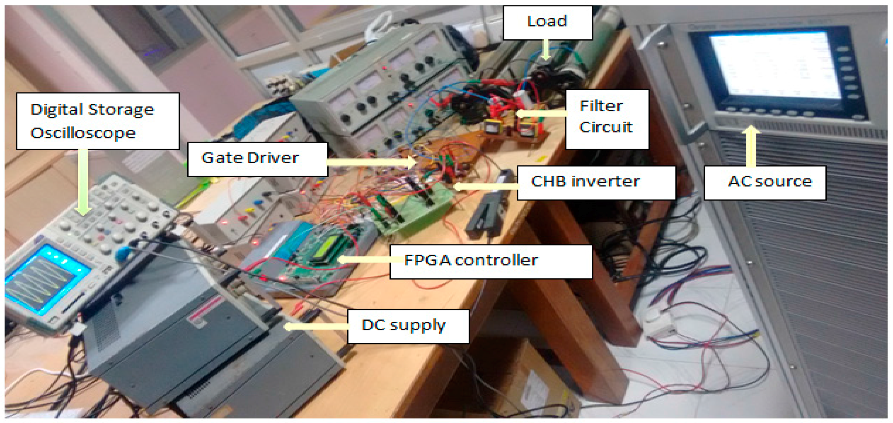
4. Experimental Results
With reference to the design procedure outlined in
Section 2, a laboratory setup of a 1 kW five-level CHB inverter based on FPGA processor is developed as per specifications in
Table 1 and
Table 2. The grid is simulated using a programmable ac source (Chroma 61511). The filter parameter selection is based on the aforementioned design described in
Section 2. PDPWM technique is employed to generate switching pulses for the inverter. The hardware implementation of PDPWM using FPGA offers computational simplicity, fast prototyping, simple hardware and software design. An image of the experiment set up is shown in
Figure 12.
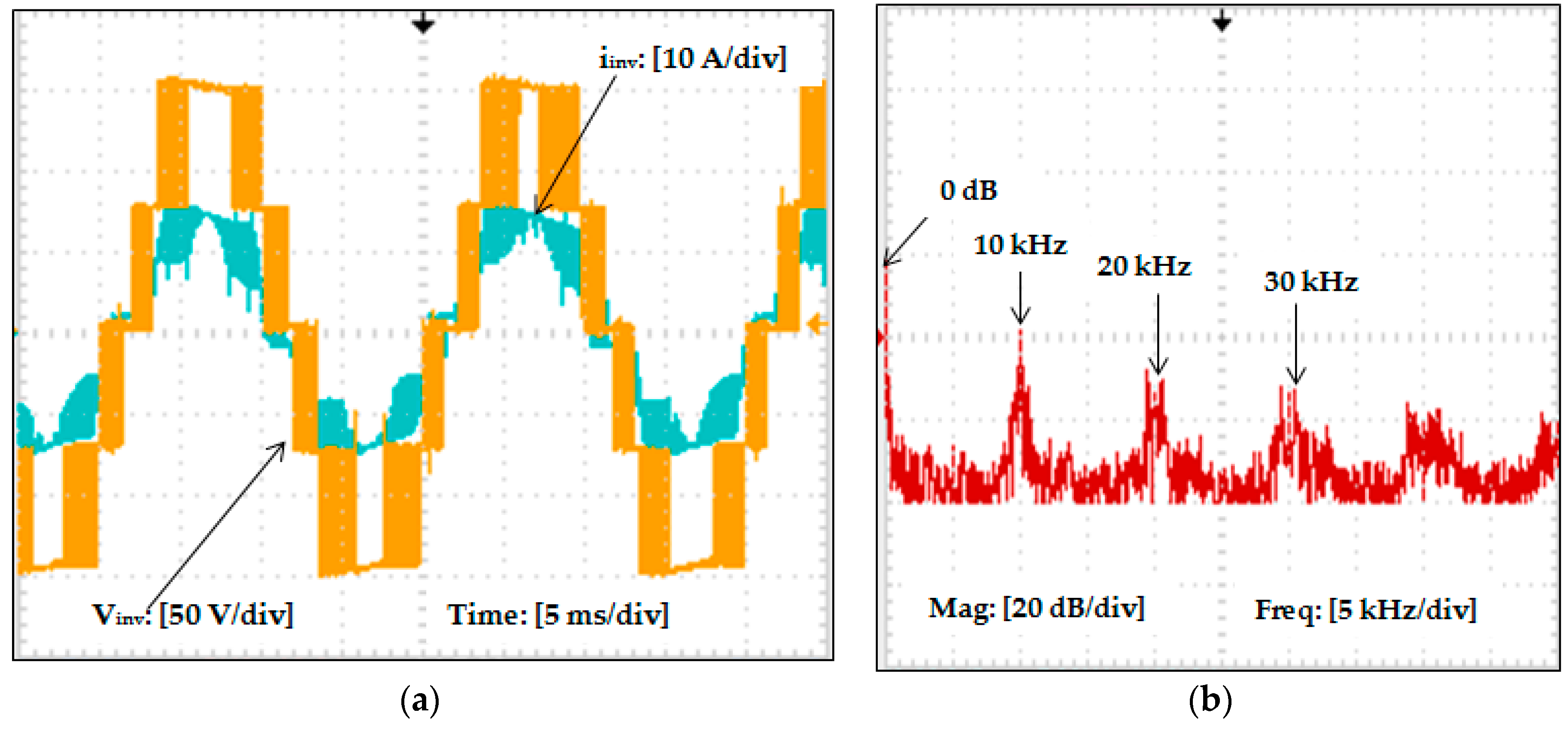
The experimental output voltage/current waveforms, which are captured before connecting the proposed passive filter to the inverter output, are shown in
Figure 13a, and the corresponding spectrum of the inverter output current is shown in
Figure 13b. As expected, the waveforms in
Figure 13a show a five-level inverter output. From the harmonic spectrum, it is evident that the uppermost harmonics of the five-level inverter output current are around the switching frequency of 10 kHz. The spectrum presents harmonic components not only at the switching frequency and respective multiples (20 kHz, 30 kHz, 40 kHz, etc.) but also in the neighborhood of these frequencies in the form of sidebands. The THD content on the output current waveform is measured as 26.90% before connecting the proposed passive filter.
The proposed filter structure is designed to attenuate the higher order harmonics from the inverter output. Experiments are carried out to compare the performance of the proposed filter with two other passive filter configurations. The experimental output waveforms and the current harmonic spectra obtained by connecting the passive filters are shown in
Figure 14,
Figure 15 and
Figure 16. Filter I is the resistive damped LCL filter strategy shown in
Figure 14. Filter II is the
Rd-
Cd damped LCL filter configuration shown in
Figure 15. Filter III is the proposed filter strategy shown in
Figure 16. In
Figure 13b,
Figure 14b,
Figure 15b and
Figure 16b, the significant harmonics of the output currents are highlighted. It can be inferred from the spectra of
Figure 13b,
Figure 14b,
Figure 15b and
Figure 16b that, before connecting the passive filter, the inverter output has the maximum harmonic amplitude lying at the switching frequency of 10 kHz. With the implementation of passive filter, the current harmonic components are reduced by a factor of nearly 6 dB/Hz from Filter II to Filter III and by a factor of almost 12 dB/Hz from Filter I to Filter III at the switching frequency of 10 kHz. With the proposed filter, the percentage of harmonics in the high frequency band (in and around multiples of switching frequency) is reduced compared to the spectra of Filter I and Filter II, showing that the proposed filter has better harmonic attenuating effect in the high frequency band.
From the spectra of
Figure 14b,
Figure 15b and
Figure 16b, the amplitudes of the dominant harmonic current (greater than or equal to 35th) are listed in
Table 5 for all three filters. It can be seen that the dominating harmonic current meets the IEEE recommendations in Filter III. The measured THD for the three filters is depicted in
Table 5, which shows that the inverter output current with Filter III has the lowest THD of 0.82%.
With Filter I, the amplitude of the harmonics at the switching frequency of 10 kHz is measured as 0.47% of fundamental; with Filter II, the harmonic amplitude at the switching frequency is measured to be 0.29% of fundamental; and, with Filter III, the harmonic amplitude at the switching frequency is measured to be 0.18% of fundamental. The amplitude of the harmonics (percent of the fundamental current) at the switching frequency, and twice, thrice, four times and five times the switching frequency with all the three filters are listed in
Table 6.
Observing the output waveforms and the harmonic spectra in
Figure 16, it can be seen that the designed filter has good attenuation effects on the harmonics. The percentage magnitude of harmonics around the switching frequency (10 kHz) is greatly reduced. The output waveforms have become sinusoidal and the THD content on the inverter output current is measured as 0.82% after connecting the proposed filter.
Figure 17a–c shows the measured damping branch currents obtained with all three filters when the output voltage is 110 V. The RMS values of the damping branch currents (
idam) are measured as 353 mA, 237 mA and 138 mA with Filter I, Filter II and Filter III, respectively. Thus, the loss in the damping circuit is computed as 2.49 W, 1.12 W and 0.17 W for Filter I, Filter II and Filter III, respectively, which is in very close agreement with the theoretical analysis.
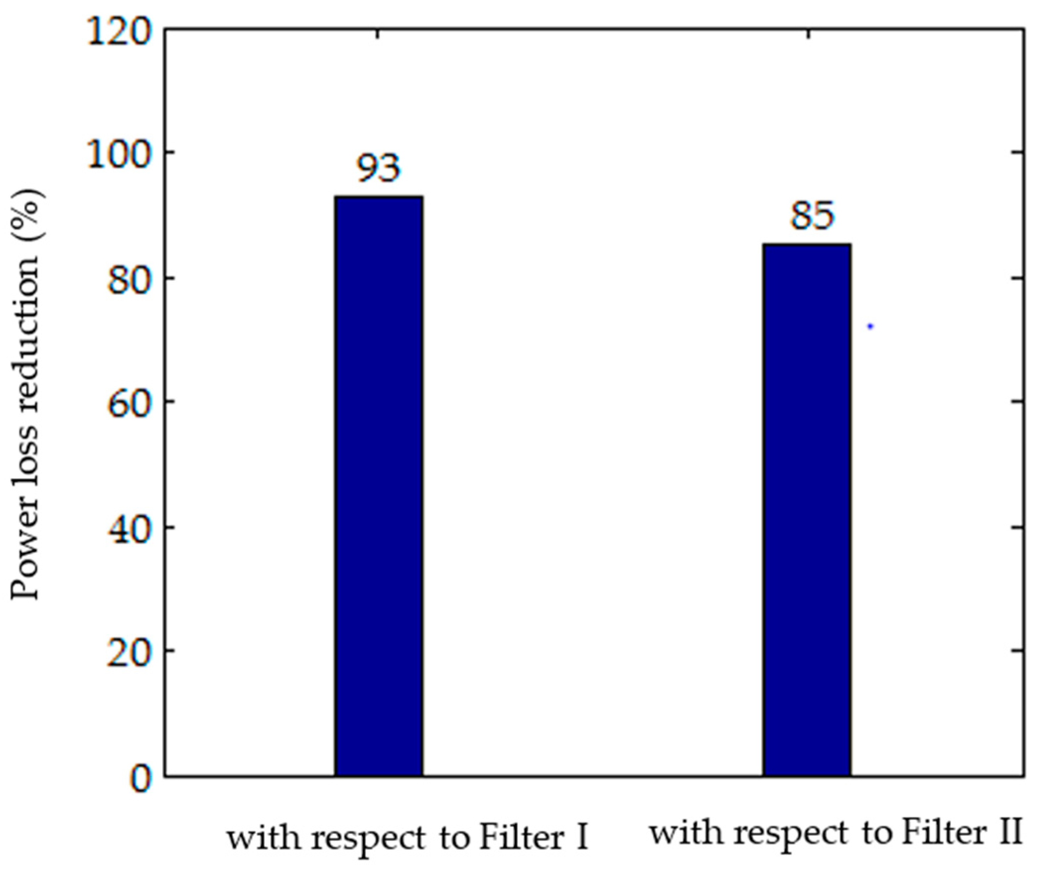
The percentage damping loss reduction achieved with the proposed filter structure with respect to Filter I and Filter II is shown in
Figure 18. It is clear in
Figure 18 that Filter III achieves 93% damping power loss reduction with respect to Filter I. With respect to Filter II, 85% damping power loss reduction is achieved, which is in good agreement with the theoretical analysis.


