Loss Model and Efficiency Analysis of Tram Auxiliary Converter Based on a SiC Device


School of Electrical Engineering, Beijing Jiaotong University, Beijing 100044, China
*
Author to whom correspondence should be addressed.
Energies 2017, 10(12), 2018; https://doi.org/10.3390/en10122018
Submission received: 9 October 2017
/
Revised: 25 November 2017
/
Accepted: 27 November 2017
/
Published: 1 December 2017
(This article belongs to the Special Issue Emerging Power Electronics Technologies for Power Systems and Machine Drives)
Abstract
:Currently, the auxiliary converter in the auxiliary power supply system of a modern tram adopts Si IGBT as its switching device and with the 1700 V/225 A SiC MOSFET module commercially available from Cree, an auxiliary converter using all SiC devices is now possible. A SiC auxiliary converter prototype is developed during this study. The author(s) derive the loss calculation formula of the SiC auxiliary converter according to the system topology and principle and each part loss in this system can be calculated based on the device datasheet. Then, the static and dynamic characteristics of the SiC MOSFET module used in the system are tested, which aids in fully understanding the performance of the SiC devices and provides data support for the establishment of the PLECS loss simulation model. Additionally, according to the actual circuit parameters, the PLECS loss simulation model is set up. This simulation model can simulate the actual operating conditions of the auxiliary converter system and calculate the loss of each switching device. Finally, the loss of the SiC auxiliary converter prototype is measured and through comparison it is found that the loss calculation theory and PLECS loss simulation model is valuable. Furthermore, the thermal images of the system can prove the conclusion about loss distribution to some extent. Moreover, these two methods have the advantages of less variables and fast calculation for high power applications. The loss models may aid in optimizing the switching frequency and improving the efficiency of the system.
1. Introduction
The power supply system in trams includes two parts, the traction power supply system and the auxiliary power supply system. The traction power supply system serves the traction motors. The auxiliary power supply system is tasked with all the auxiliary devices including air conditioners, compressors, fans, etcetera but not the main circuit of the traction system. An important component of the auxiliary power supply system is the auxiliary converter, the capacity of which is typically tens of kilovolts, the bus voltage is 750 V and the outputs are AC 380 V and AC 220 V. Therefore, the reliability of the auxiliary converter plays an important role in the smooth operation of the vehicle. Since the auxiliary converter is a necessary part of vehicle equipment, its weight and volume have been a focus of great attention [1,2,3,4,5,6].
When designing an auxiliary converter, the circuit topology must first be determined. Since the DC bus voltage of the tram is 750 V, there are two types of commonly used topology, namely a power frequency isolation scheme and a high frequency isolation scheme. The power frequency isolation scheme is just a three-phase inverter, which directly inverts DC 750 V into a three-phase AC output. This scheme has the advantages of simple control and a low number of switching devices; at the same time, its most significant drawbacks are the larger size and weight of its three-phase isolation transformer. The high frequency isolation scheme has a high-frequency DC/DC converter and a three-phase inverter. The number of switching devices is increased but the size and weight of the transformer are significantly reduced, in this scheme. Therefore, the auxiliary converter in this paper adopts the high frequency isolation scheme for a maximum power density.
The width of the drift region of the SiC device is smaller than that of the Si device for the same breakdown voltage, because the doping concentration of the drift region is higher. The smaller depletion width reduces the on-resistance of the SiC device, thereby reducing conduction losses [7,8,9,10,11]. Therefore, with the advent of SiC technology, the MOSFET on-resistance also decreases, even at higher voltages. Recently, silicon carbide devices for very high voltage applications have been developed [12,13,14,15]. The switching frequency of the SiC MOSFET high-power converter is higher than those of silicon IGBTs, with its lower conduction losses, combined with its inherent low switching losses, which achieves the benefit of working with smaller filter components [16,17,18]. Scholars also have performed a large number of studies for medium and low voltage applications. When Si IGBTs are replaced with SiC MOSFETs in a converter, the efficiency will increase in varying degrees [19,20,21]. A 50 kW PV string inverter was designed with SiC devices [22]. However, these papers just completed the experiments and got the differences between Si and SiC devices without a theoretical analysis of system loss. Regarding device loss calculation, scholars have done a lot of work. An accurate analytical loss model which considered the package and PCB parasitic elements in the circuits was evaluated [23]. The power losses of the DAB DC/DC converter were analyzed [24], where the author considered the ideal waveform in circuit. However, these two articles consider many factors that are not suitable for a high-power system analysis. The overall power loss of the DC/DC converter was studied [25] but the author did not give a detailed calculation formula of device loss in the system. There is no investigation of the loss calculation of a DC/DC converter in DCM mode, from the results of a literature research.
A SiC converter prototype whose topology is a high-frequency DC/DC converter (which works in DCM mode due to minimum inductance in system) plus a three-phase inverter is designed for the auxiliary converter in the trams, in this paper. To meet the need for a fast estimation of device loss in Engineering, loss calculation formulas for high power applications according to the working principle of the prototype circuit are derived. First, according to the circuit topology and principle, the loss formulas of each module in the auxiliary converter are deduced and the loss of each module could be calculated by formulas. Then, some characteristics of the SiC devices used in the system are tested, including the saturation voltage drop of the MOSFET, the forward voltage drop of the diode and the switching loss of the MOSFET. The aims of the study are to understand the practical application characteristics of the SiC devices and to provide data support for the PLECS loss simulation model. The PLECS loss simulation model is built according to the actual parameters of the auxiliary converter. Finally, the losses of each module are measured through the experiments of the auxiliary converter prototype. Comparing the theoretical calculated values, model simulated values and experimental measurement values, the losses of each module are shown to be basically consistent with each other. It is confirmed that the loss calculation theory and the loss simulation model is valuable. The loss calculation theory and the loss simulation model can provide a reference for follow-up optimization work, which can in turn reduce the workload of the subsequent optimization.
2. The Loss Estimation Equation of Auxiliary Converter
2.1. Overview of Auxiliary Converters
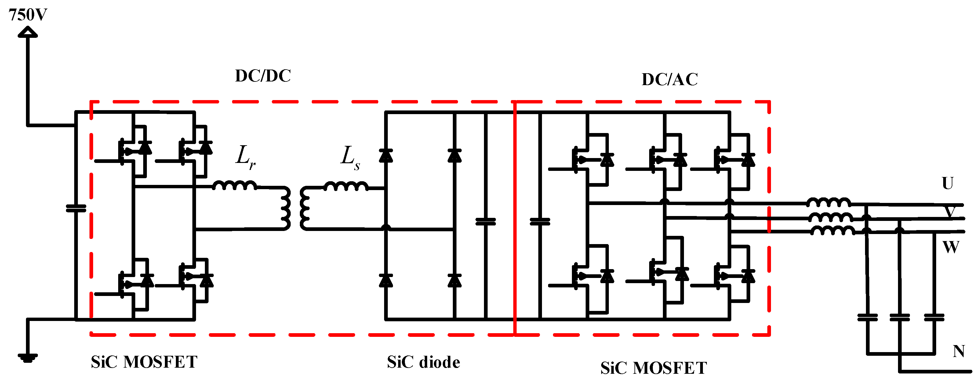
In this paper, the topology structure of the SiC auxiliary converter is high-frequency DC/DC plus three-phase inverter. There is no filter inductance on the output side of the high frequency DC/DC module, which is different from the traditional DC/DC converter. The DC/DC converter works at DCM mode. The circuit is shown in Figure 1 and the system parameters are shown in Table 1.
The high frequency and high temperature characteristics of SiC MOSFETs result in them being widely used in converters. However, under high frequency operation conditions, SiC devices still involve large power loss during the switching process. An accurate loss estimation method of the system is quite important for the switching frequency selection, cooling module design and efficiency promotion of the overall system.
2.2. Principles of Device Loss
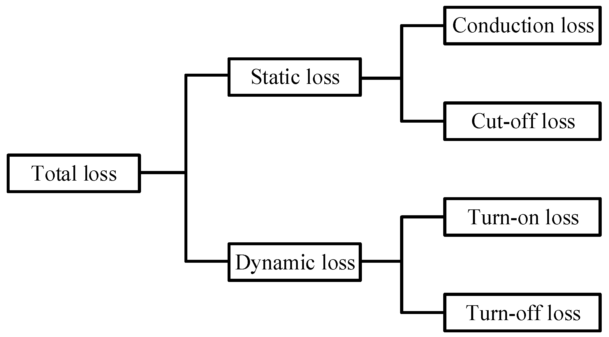
The components of SiC MOSFET’s loss are shown, as the switching elements in the auxiliary converter, in Figure 2.
Due to the leakage current of the SiC device in the blocking state being negligible, the loss mainly includes the on-state loss , turn-on loss and turn-off loss .
Concerning the case of high power applications, the on-state loss of the device in a single cycle can be determined by its equivalent resistance and the effective value of the through current. The average on-state loss can be multiplied by the frequency based on the single cycle loss. Thus, the on-state loss calculation formula for simple calculation can be derived.
Using the formula, is the RMS value of the current flowing through the device; is the on-state resistance of the device.
Figure 3 shows [24] the turn-on switching energy are determined by the voltage and current at the time of switching and time interval during switching ON. The same is true for the calculation of the turn-off switching energy .
It can be determined that the switching energies at different power conditions are linearly related to the operating time voltage and current when dealing with high power applications. Based on the datasheet from the manufacturer, the single switching energies and of the device under specific test voltage and current can be known. Then, the switching losses through single switching energy and switching frequency can be discerned:
Regarding the formulas, and are the loss of turn on and turn off in the datasheet at the standard test condition; and are the blocking voltage and collector current in the datasheet at the standard test condition; and are the blocking voltage and collector current at the actual condition and is the switching frequency.
2.3. Loss Estimation of High Frequency DC/DC Converter
Using the high frequency DC/DC module, there is no filter inductance in the output side, thus the transformer current is intermittent, meaning the high frequency DC/DC converter in this paper works in DCM mode and the current waveform is different from that in the traditional DC/DC converter working in CCM mode. Therefore, it is necessary to analyze the working principle of the DC/DC module to get the loss estimation formula. The main waveforms of full-bridge converter are shown in Figure 4 and, because the current waveform of the transformer is centrosymmetric, the author only need to analyze the operation states of the t0–t3 period, while is the beginning of the next cycle.
Figure 4 shows Q1–Q4 are four switching devices. is the pulse of switching devices. The red line represents the primary side current of the transformer. The purple line represents the primary voltage of the transformer. Ideally, the primary side current of the transformer has three states. During Stage 1, the primary voltage of the transformer is system input voltage and the current rises linearly. Through Stage 2, the primary voltage of the transformer is zero due to the phase shift angle and the current drops linearly. During Stage 3, due to the large phase shift angle, the primary side current of the transformer remains zero. It can be determined that the formula of the transformer’s primary current is as follows:
Formula (5) shows the specific system power and switching frequency (or cycle). The constraints are as follows:
Regarding the formulas, Vin is the input voltage of the full-bridge converter; is the primary leakage inductance of the transformer; Ls is the secondary leakage inductance of the transformer; is the output voltage of the full-bridge converter; is the switching period of the full-bridge converter; K is the transformer ratio and P is the power of the converter.
Formulas (5) and (6) demonstrate the key parameters in the schematic diagram can be solved, including , and Based on the above analysis, the loss calculation formulas of the switching devices in the full-bridge converter and rectifier can be determined.
Ignoring the dead time, the on-state loss formulas of the switches in the first half of the cycle are as follows:
The integral calculation in Formulas (7)–(9) is relatively simple, thus no detailed calculation process is given here. Additionally, the on-state loss in the second half of the cycle is the same, thus the full-bridge inverter has a total on-state loss.
While the current is in the intermittent state, the current of and devices are zero when they turn on and turn off and the switching loss is nearly zero. Therefore, the switching losses of and are as follows:
The total switching loss of the full-bridge inverter is as follows:
Since the SiC diode has very little reverse recovery loss, the loss of the rectifier is only the on-state loss of diode. The on-state loss of the rectifier diode can be calculated by using the secondary side current of the transformer. There is a linear relationship between the primary side current and the secondary side current of the transformer, which is determined by the transformer ratio K. Then, the on-state loss of a single diode is calculated as follows:
where is the on-state voltage drop of the diode. Therefore, the total loss of the rectifier is as follows:
2.4. Loss Estimation of Three-Phase Inverter
The commonly used control strategies of inverters are SPWM (sinusoidal pulse width modulation) and SVPWM (space vector pulse modulation) and the structure and principle of three-phase two-level inverters have also been analyzed in detail in many previous studies [24]. The loss of the inverter in the SPWM modulation mode is analyzed in this paper.
Based on SPWM modulation shown in Figure 5, the modulation function and load current function are as follows:
where m is the modulation ratio, is the power factor angle and Im is the maximum value of the output current of the inverter.
The dead time can be ignored, due to the high-frequency characteristics of the SiC device, thus in a switching cycle , the conduction time of the MOSFET and diode , can be expressed as follows:
During a carrier cycle, the current changes very little and the current can be regarded as the current of the output side, since the AC side relates to the load. Figure 6 is a diagram about the output phase voltage and the phase current of the inverter according to Formula (16). The area where the current is positive needs to be calculated.
The on-state loss of the MOSFET is as follows:
The on-state loss of the anti-parallel diode is as follows:
Formulas (18) and (19) are calculated separately:
The power losses of these three bridge arms are the same, thus the total on-state loss of the two-level inverter in the SPWM modulation is shown as follows:
The switching loss of devices can be expressed as follows:
where , are the turn-on and turn-off energy losses at a certain time, is the frequency output of current and N = fs/fout. When the N is very large (i.e., the carrier frequency is much larger than the fundamental frequency), Formula (23) can be expressed as an integral. Then we simply need to calculate the area where the current is positive, then the switching loss of the single switch is as follows:
thus, the total switching loss of the three-phase inverter is:
The formula method must use the precise analysis of the circuit principle and the data of the datasheet of the SiC MOSFET device. However, the formula method also has the shortcoming that the device data are measurement data under ideal conditions and are different from data measured under practical application conditions. Additionally, the formula method can only estimate the system loss under a certain condition, once the key parameters of the system have changed, the loss estimation must be repeated, which results in time-consuming and laborious optimization work.
3. The Loss Estimation by Experimental Parameter Extraction and Simulation Model
To facilitate the selection of the switching frequency and efficiency improvement of the converter, it is necessary to establish an effective loss model which can be easily generalized. The mockup of the converter system is replicated using PLECS simulation software. The software has the advantage of model simulation, which makes it possible and easy to measure the on-state loss and switching loss of the switching device by using the probe module, according to the data of the switching device. Additionally, combining the cycle mean value unit and periodic pulse mean module in the PLECS module library with the probe component, the software can transform the instantaneous value of loss into the average loss and can express the average loss intuitively, which facilitates the generalization of the model.
3.1. The Characteristics of the 1700 V/225 A SiC MOSFET
Generally, the key parameters of the device can be found in the datasheet given by the manufacturer but the measurement environment of the manufacturer and working state of the device are very different from the actual application, thus there is a certain degree of error between the actual dynamic and static characteristics of the device and the characteristics of the datasheet. To ensure the accuracy of the loss simulation model, it is necessary to test some key parameters of the devices [25,26,27,28].
3.1.1. The Static Characteristics of SiC MOSFET by Experiment
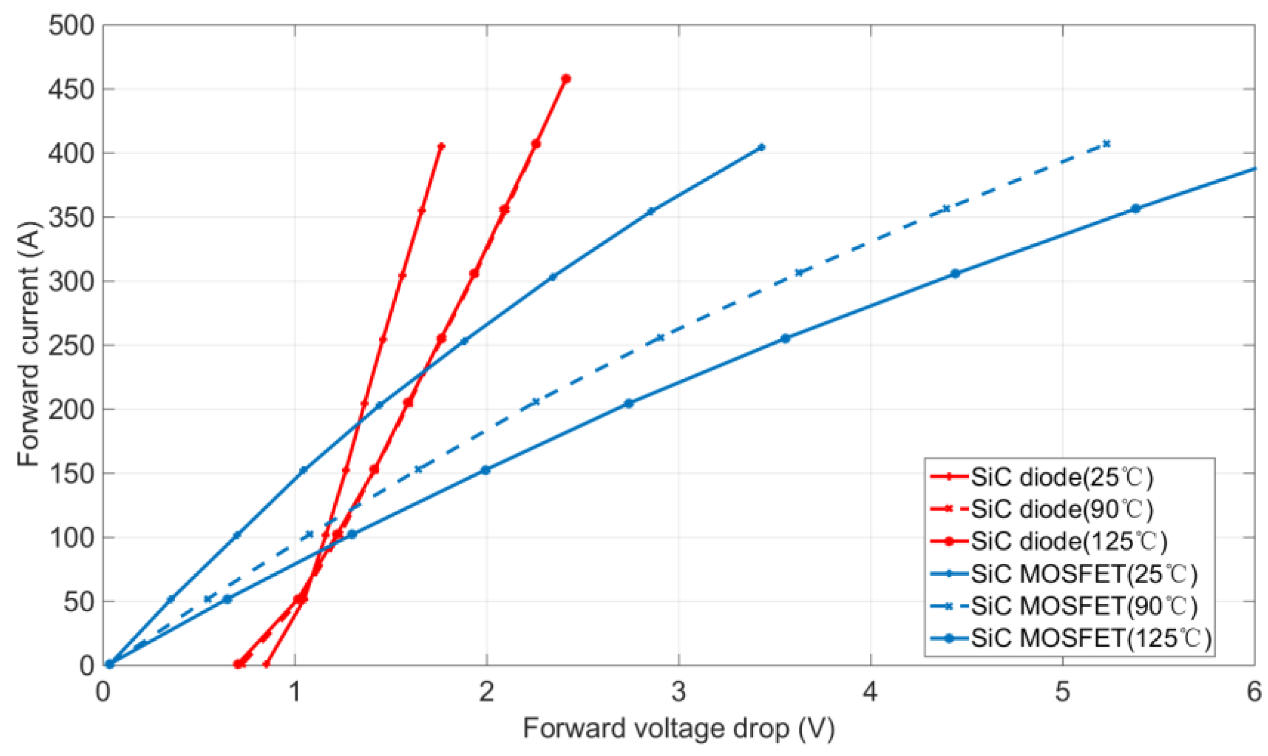
The saturation voltage drop of the SiC MOSFET and the forward voltage drop of the anti-parallel diode affect the on-state loss of the devices. Therefore, it is necessary to take precise measurements in order to ensure the accuracy of the model. Figure 7 shows the curves of the saturation voltage drop of MOSFET and forward voltage drop of the diode at different temperatures.
Figure 7 shows that the saturation voltage drop of the SiC MOSFET and forward voltage drop of the anti-parallel diode are increasing as the temperature increases. This will lead to the on-state loss increasing, in practical applications, at which time it can be seen that the change of the MOSFET saturation voltage drop becomes significant. Concurrently, under the condition of the same temperature, the saturation voltage drop increases with the increase of current passing through the device, as expected.
3.1.2. The Dynamic Characteristics of SiC MOSFET by Experiment
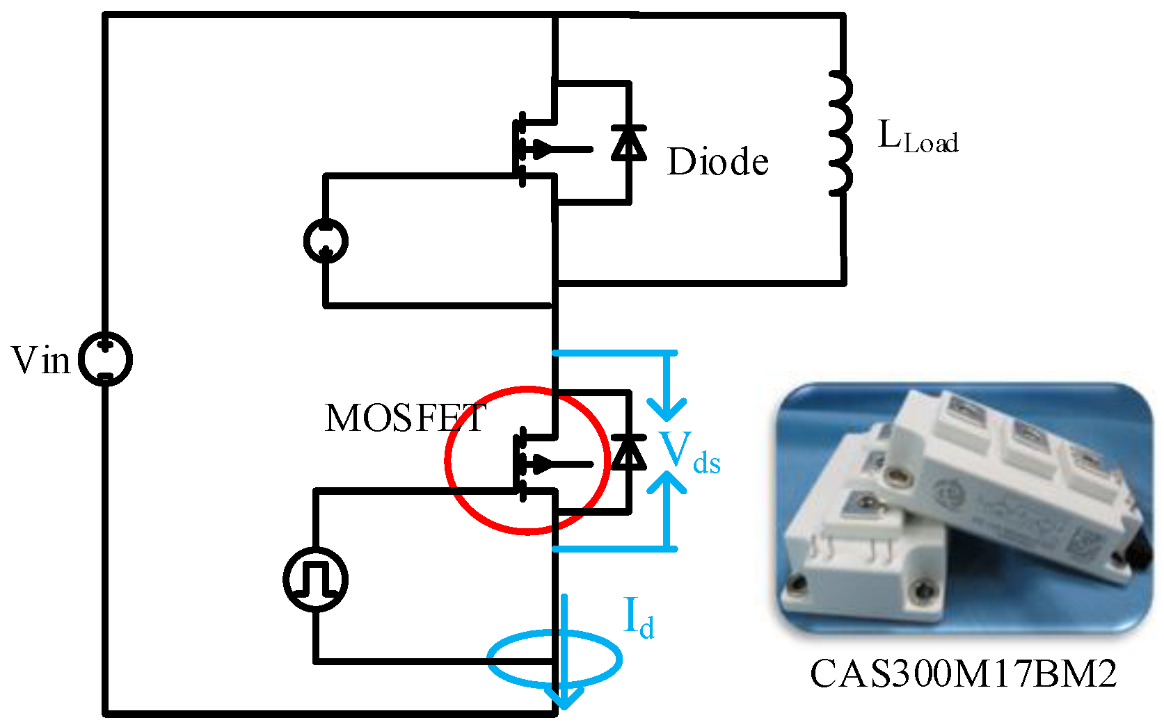
To accurately grasp the dynamic performance of SiC devices, the selected SiC devices are tested by means of a double pulse test platform. The double pulse test circuit is shown in Figure 8. The circuit adopts a single-arm structure and the test object of the MOSFET module is shown in the figure. Then, the and of the device, under certain conditions, are calculated by measuring the and of the SiC MOSFET in the red circle.
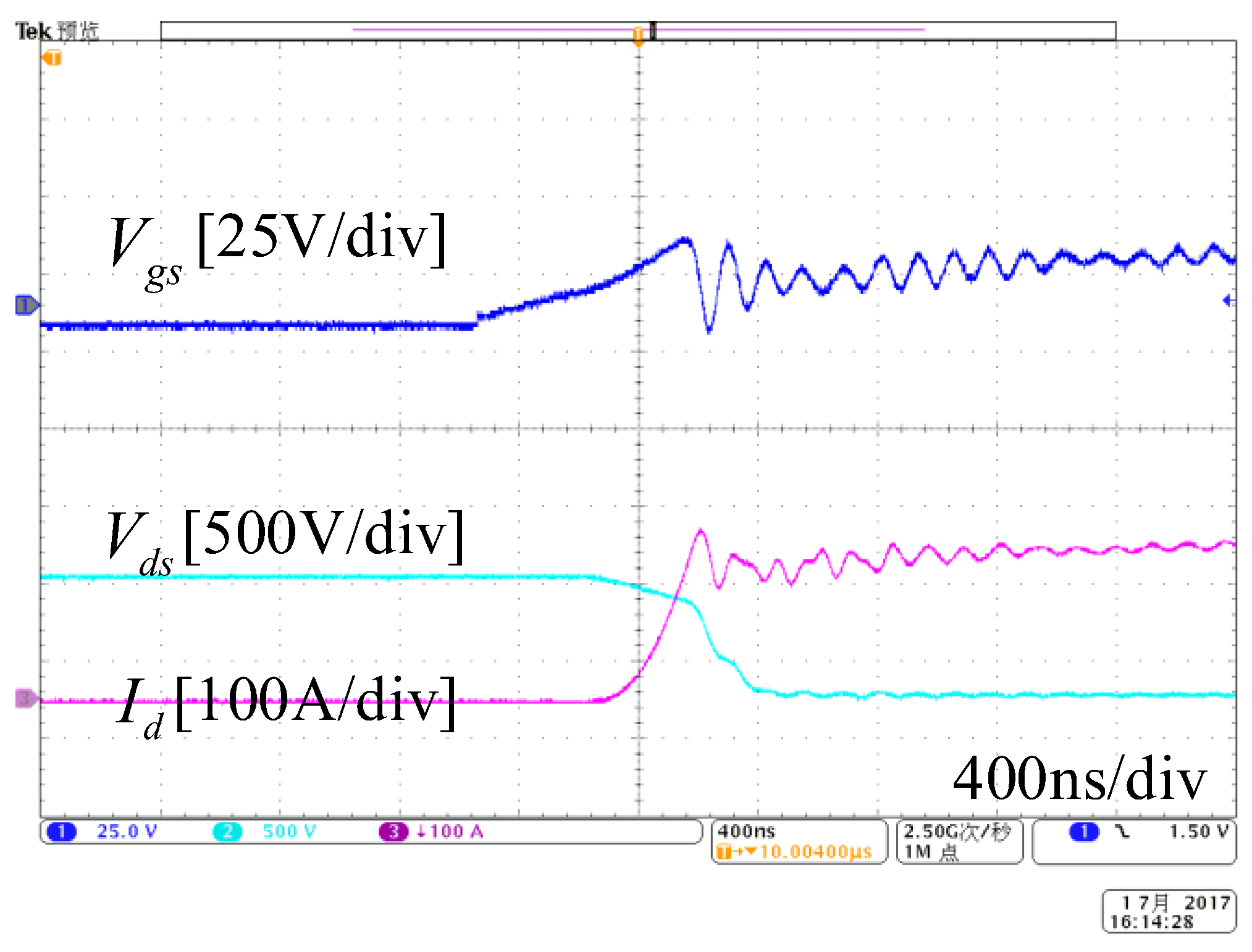
Figure 9 shows the DP test waveform. Concluding the first pulse, the inductor current reaches the desired device current of the test and the device is tested for turn-off characteristics. During the OFF condition of the device, the inductor current free wheels through FWD and remains almost the same until the next ON pulse. When the second pulse begins, the device is tested for turn-on characteristics.
The turn-on waveform at 750 V and 200 A with gate resistance of 15 Ω is shown in Figure 10. The turn-off waveform is shown in Figure 11. The single turn-on and turn-off energy of the SiC MOSFET can be calculated by the overlapping regions of voltage and current.
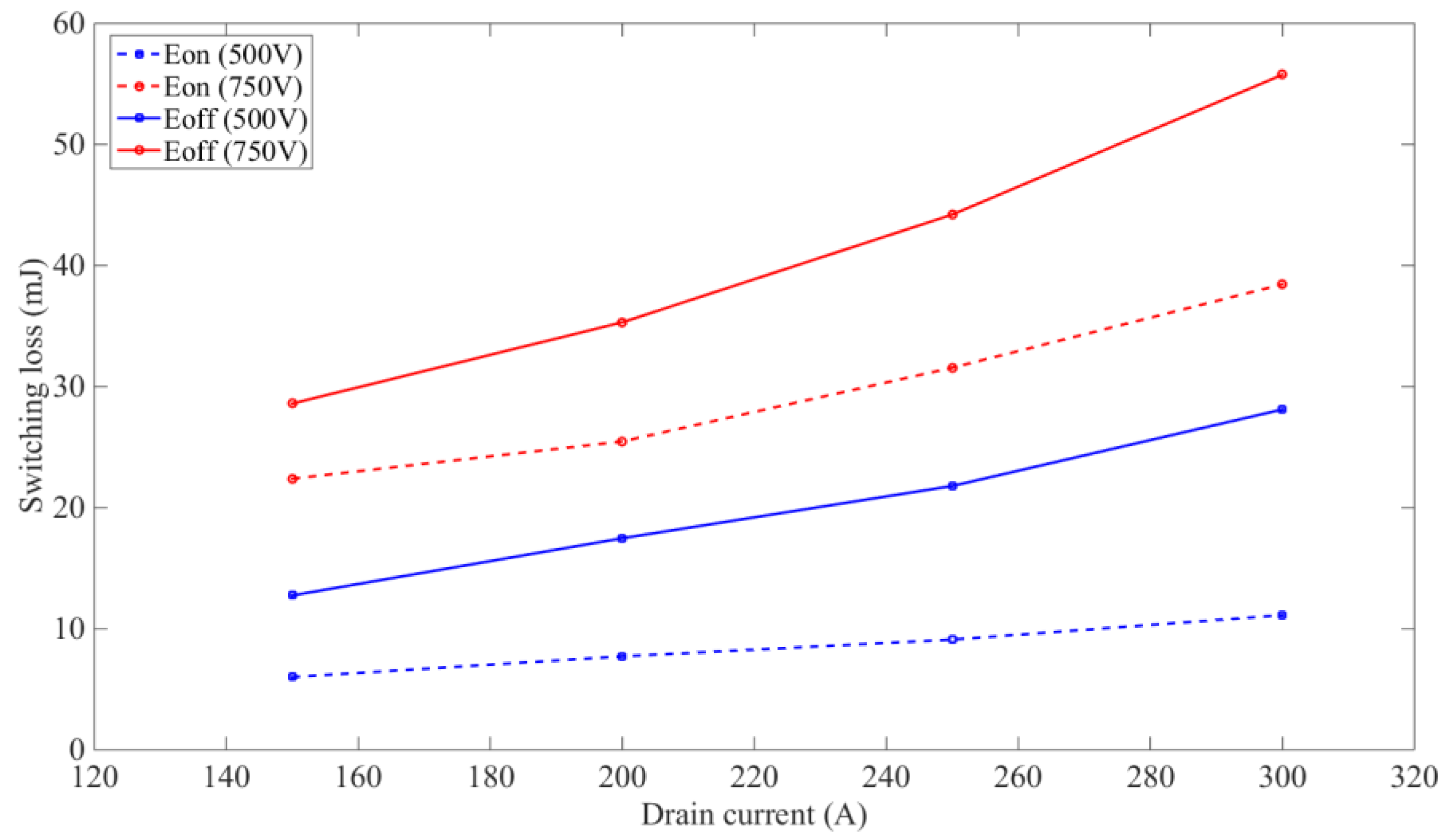
Figure 12 shows the switching energy at different device currents and voltages measured and plotted. The gate resistance is 15 Ω and hot-plate temperature is controlled at 125 °C to ensure that the junction temperature of the device is at 125 °C Both the and increase almost linearly with the current. The voltage affects the switching losses of the device proportionally.
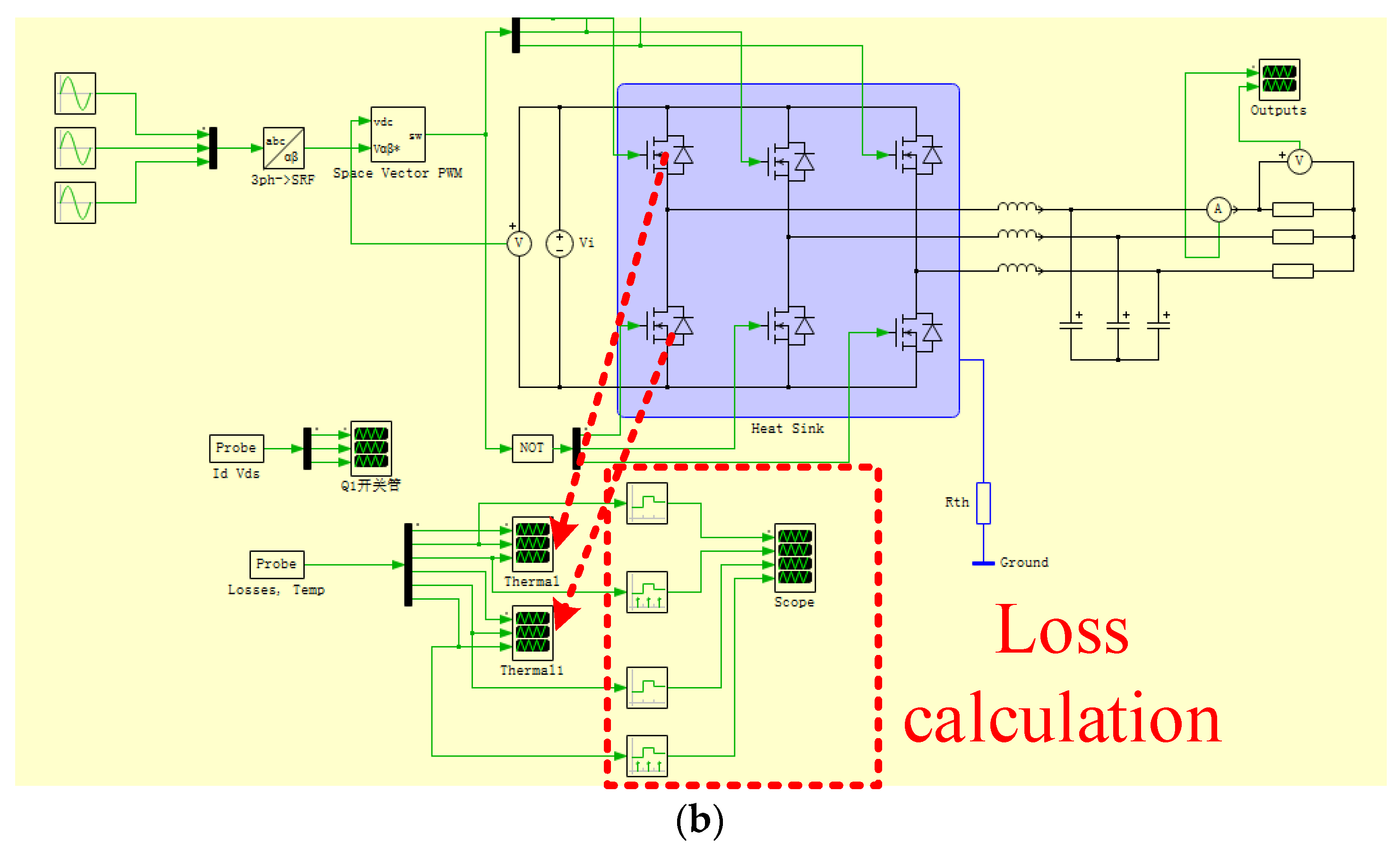
3.2. The PLECS Simulation Model
The boundaries of the simulation use the actual system parameters, as shown in Table 1 and the switching devices (including rectifier) are all CREE’s SiC MOSFET module CAS300M17BM2. The high-frequency DC/DC converter simulation model and the three-phase inverter simulation model are shown in Figure 13. The loss of the device is determined by the actual working conditions of the circuit. The average conduction loss and average switching loss of the device can be calculated by the relevant modules in the PLECS module library.
The device test data in Section 3.1 are substituted into the device thermal description file of the loss simulation model, as shown in Figure 14. This allows the data of the dynamic and static characteristics of the switching devices to be closer to the device data for practical application.
3.3. The Results of the Formula Model and Simulation Model
According to the formulas in Section 2.3 and Section 2.4 and the conditions shown in Table 2, the theoretical calculation results of the on-state loss and switching loss of each part in the auxiliary converter system can be obtained. Comparing these with the PLECS loss simulation model values, the results shown in Table 3 can be obtained.
The on-state loss values of simulation are generally slightly greater than those of the theoretical calculations, since the device data used in the simulation are measured under actual conditions, which are slightly higher than the ideal values in the datasheet. Therefore, the on-state losses in the simulation are all slightly higher than the theoretical values. However, the results obtained by the simulation are in good agreement with theory considering the proportion and their distribution of the losses. It is thus proven that the simulation model is consistent with the theory. The actual loss of switches in the converter should be measured in the experiments to verify the validity of theory and simulation.
4. Experimental Results of SiC-Based Auxiliary Converter
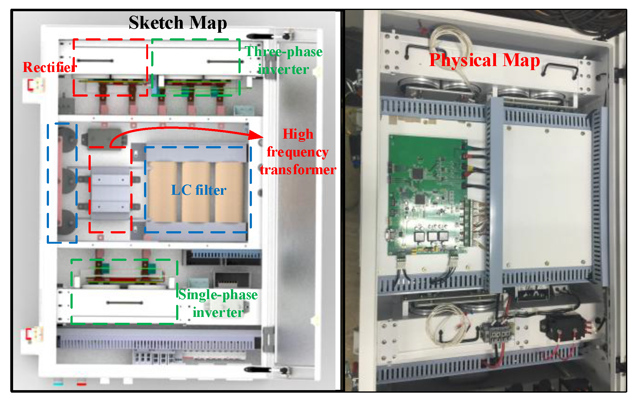
Using the SiC auxiliary converter prototype shown in Figure 15, the waveforms and losses are measured when the power of the system is about 40 kW. The prototype topology is shown in Figure 1.
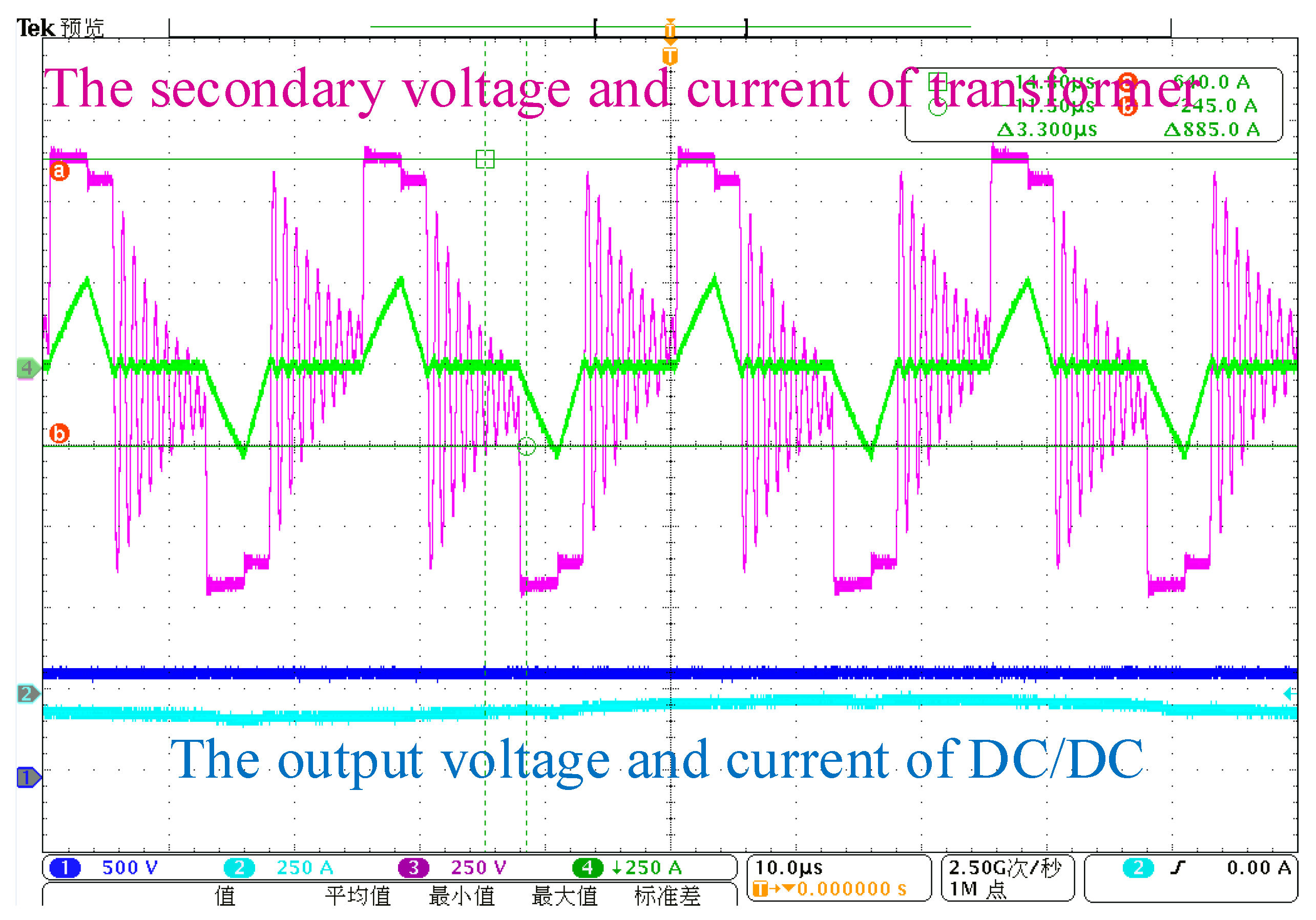
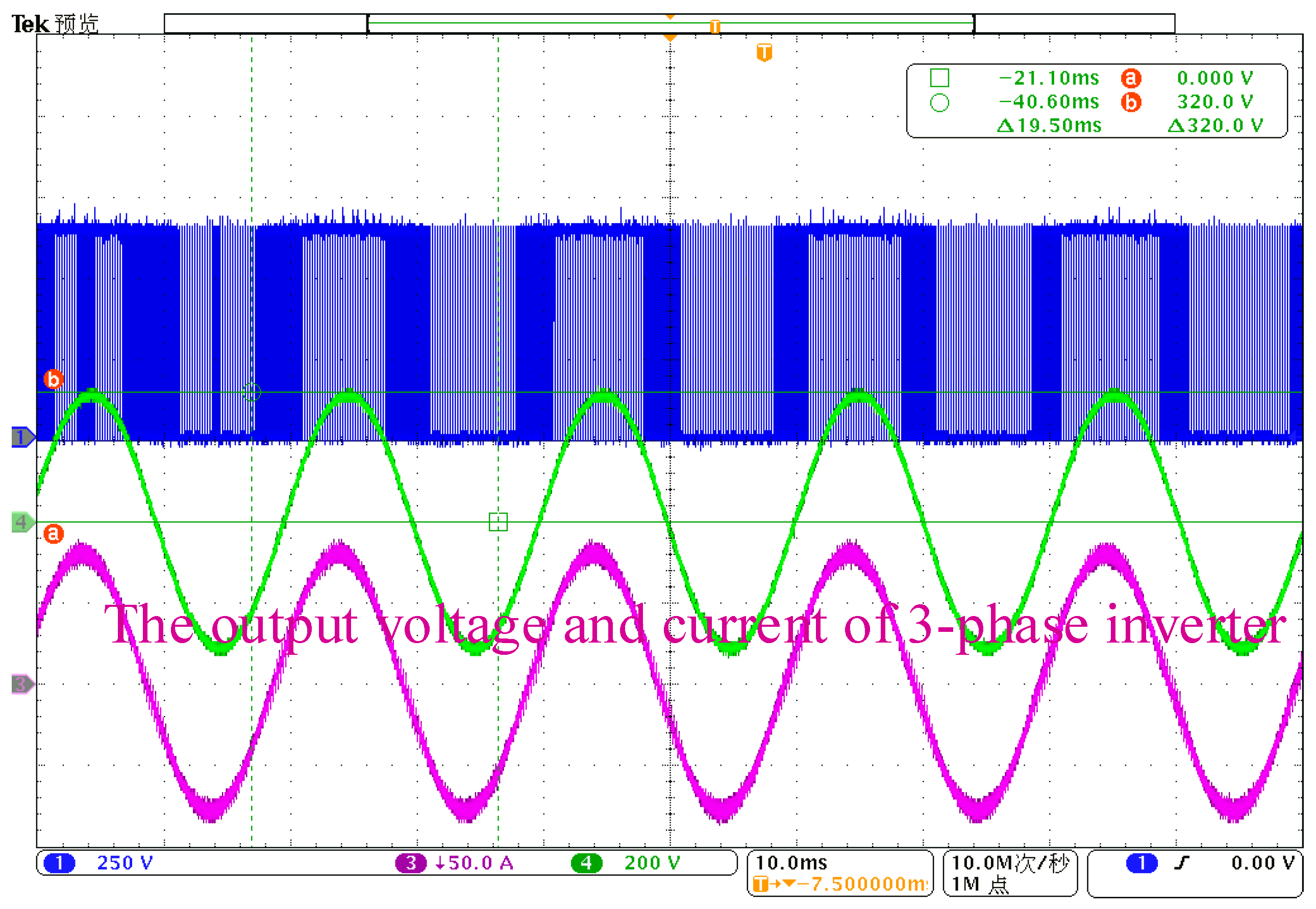
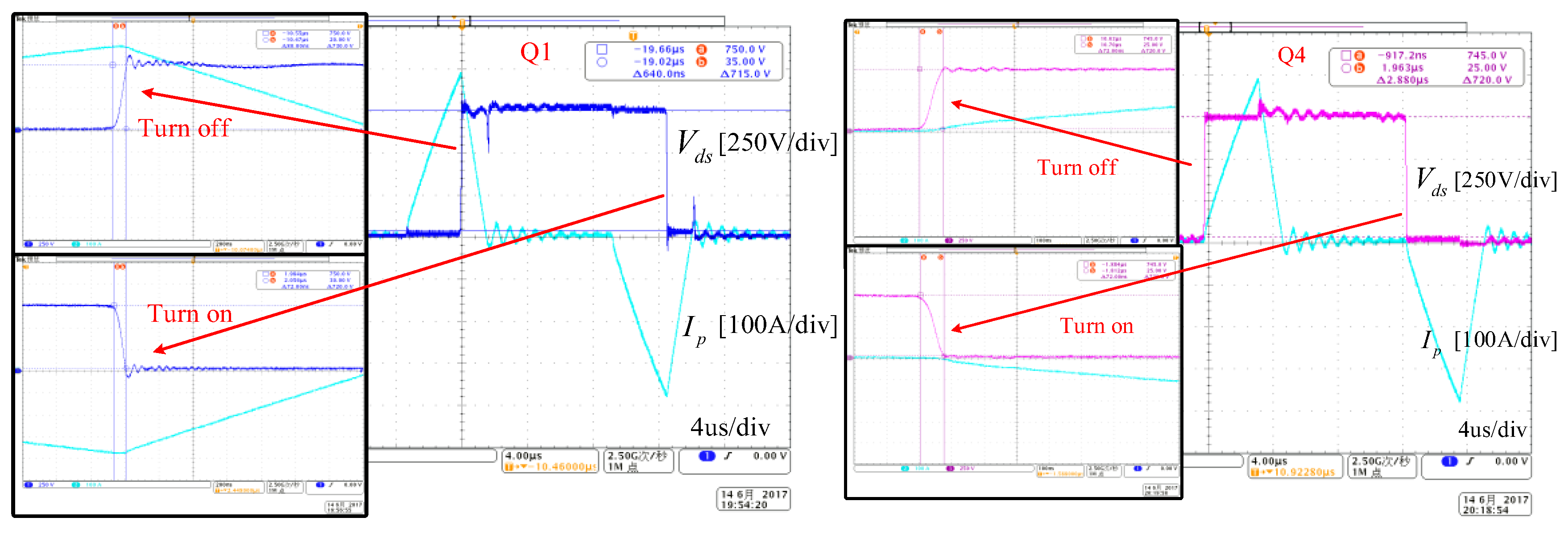
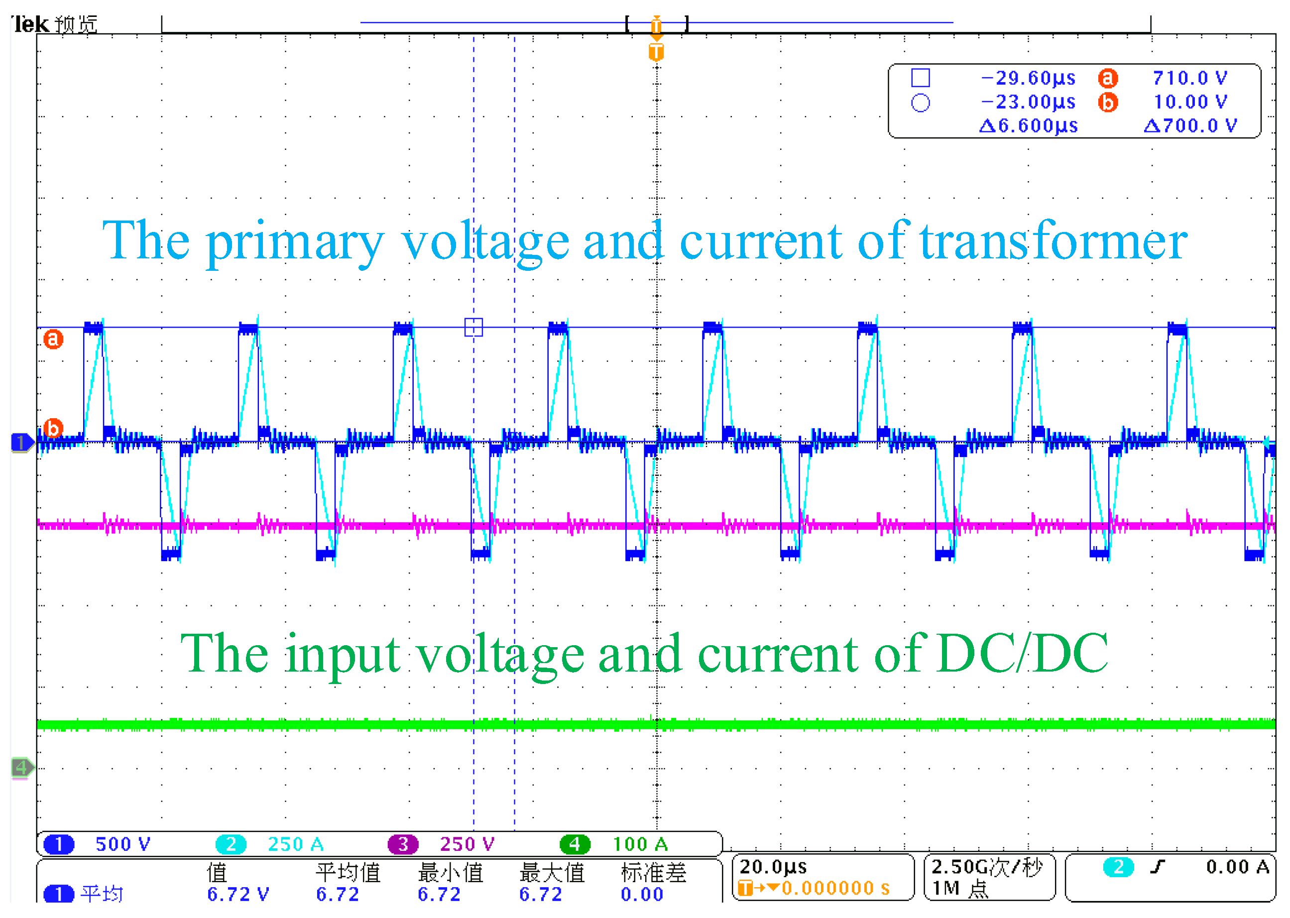
Since the switching device is the SiC module, it is impossible to observe the current through the MOSFET, thus the author measured the output current of the module. Figure 16 is the full-bridge inverter module experimental waveform with 40 kHz frequency. It can be seen from the waveform that the phase relationship between the transformer current and the switching device’s voltage is the same as the theoretical analysis. The rectifier waveform is poor, due to the voltage shock which exists during the period when the current is basically zero. The three-phase inverter module experimental waveform is ideal, with a 10-kHz switching frequency, which signifies that the output has a low voltage harmonic content, as shown in Figure 17.
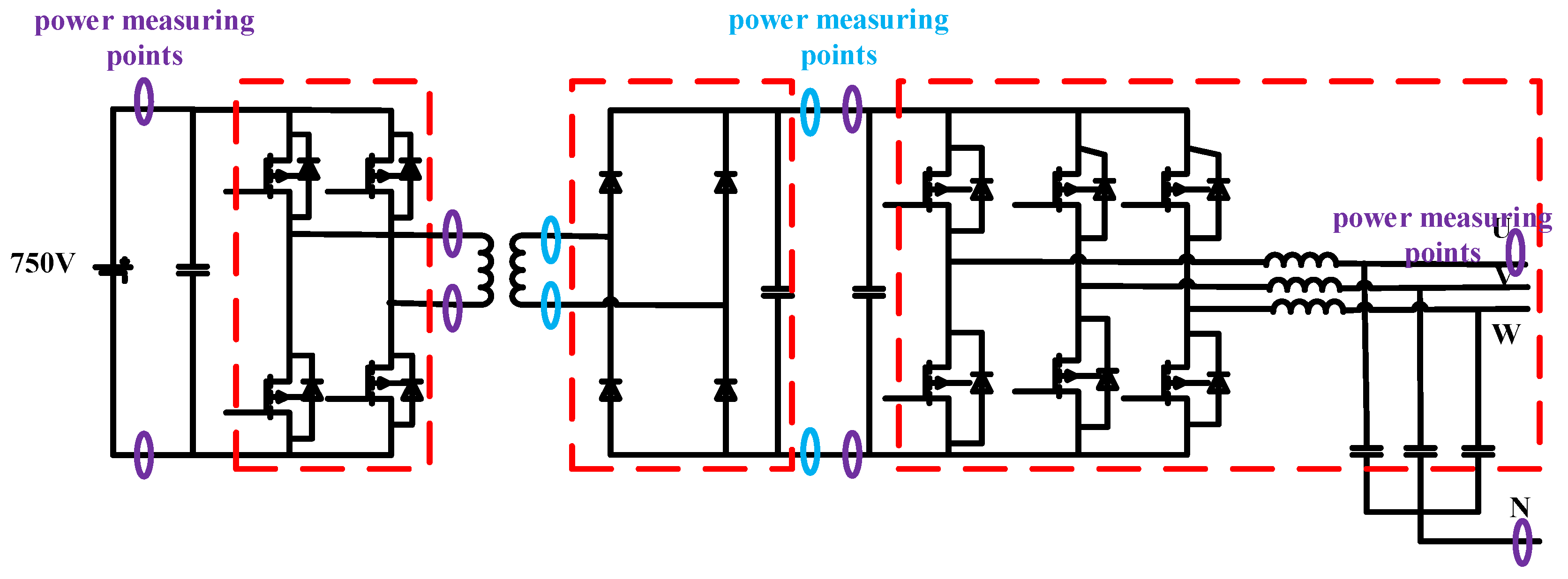
Using the module input and output power as shown in Figure 18, the total loss of each module is verified. The measurement waveforms and results revision process are shown in Appendix A. The following table is a comparison of the experimental results with the theoretical calculation values and simulated values.
Table 4 demonstrates that, overall, the simulated value is closer to the experimental value than the theoretical calculation value, which signifies that the simulation model has a higher reference value. The theoretical calculated loss of the full bridge inverter and three-phase inverter are close to the experimental value. However, there is a significant gap between the theoretical calculated value and the experimental value of the rectifier. The forward voltage of the rectifier diode, in the PLECS simulation model, used measured values while in the theoretical calculation, the forward voltage of the rectifier diode is set to a typical value from the datasheet, which makes the theoretical calculated loss of the rectifier diode slightly lower.
The above comparison table demonstrates that, overall, the simulated value is closer to the experimental value than the theoretical calculation value, which signifies that the simulation model has a higher reference value. The theoretical calculated loss of the full bridge inverter and three-phase inverter are close to the experimental value. However, there is a significant gap between the theoretical calculated value and the experimental value of the rectifier. The forward voltage of the rectifier diode, in the PLECS simulation model, used measured values while in the theoretical calculation, the forward voltage of the rectifier diode is set to a typical value from the datasheet, which makes the theoretical calculated loss of the rectifier diode slightly lower.
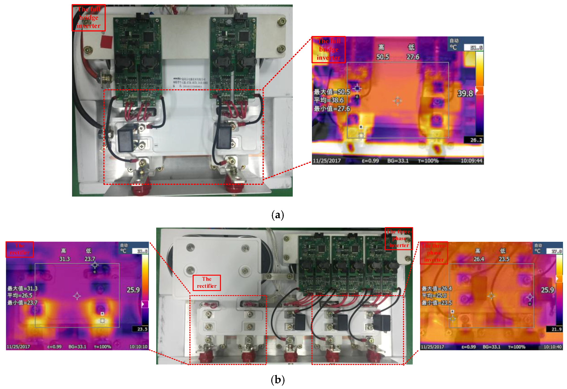
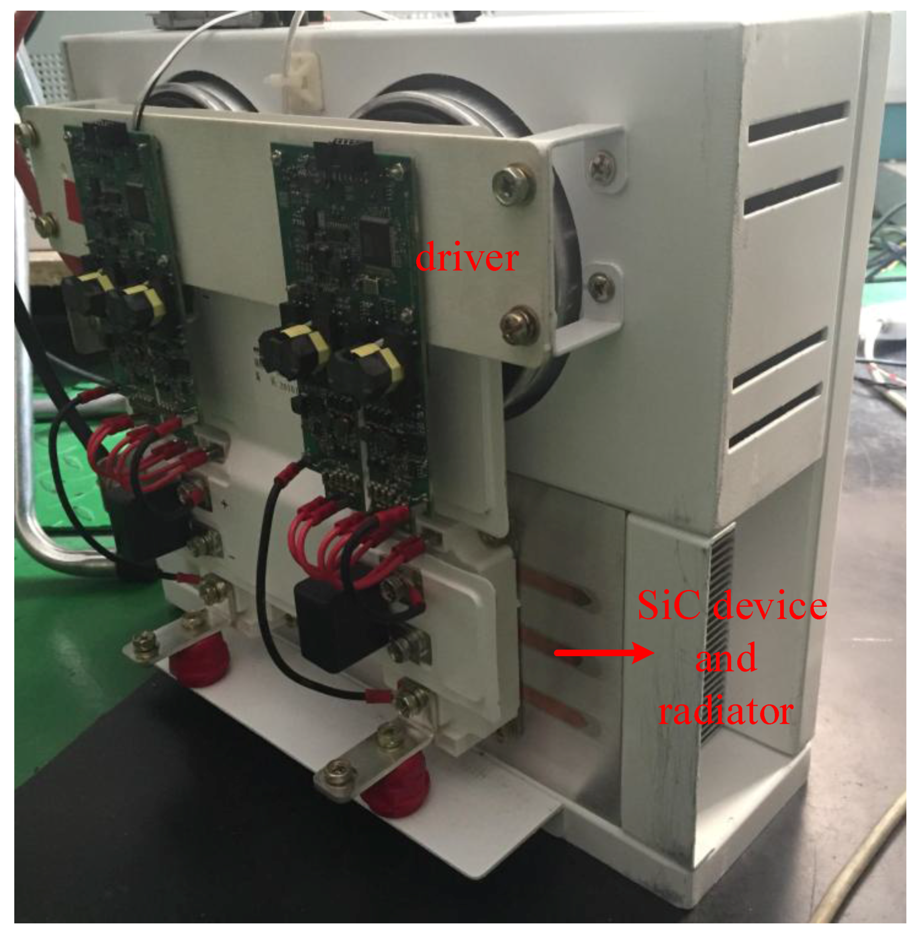
Figure 19 shows the full bridge inverter module when taken out of the system. It can be seen that the SiC device and radiator is at the bottom of the system. Once the prototype is running for a period, the full bridge inverter module, rectifier module and three-phase inverter module is removed from the system to get thermal images.
Figure 20 shows the thermal images of three modules in our system when they are removed from the system after the system running at 40 kW for a period. Our system uses forced air cooling method and it takes a few minutes for us to remove these modules from the system to get thermal images, therefore the temperature is a little lower than the actual temperature. Figure 20a shows the thermal image of the full bridge inverter module and its average temperature is at about 38.6 °C. Figure 20b shows the thermal image of the rectifier module whose average temperature is at about 26.5 °C and the thermal image of the three-phase inverter module whose average temperature is at about 25 °C. The radiators in three modules are the same, therefore their average temperatures are directly proportional to their power consumptions. It can be seen that the temperature of the full bridge inverter module is higher than the temperature of the other two modules, and the temperature of the three-phase inverter module is closer to that of the rectifier module. These differences can prove the conclusion about the loss distribution to some extent.
5. Conclusions
The main work of this paper was to establish a loss model of a tram SiC auxiliary converter. During the process of building this loss model, first, according to the circuit topology and parameters, theoretical calculation formulas of the SiC device losses for the auxiliary converter were derived. Based on the relevant parameters of the device data, the loss of each part in the system was estimated by formulas. Then, the static and static characteristics of the Cree’s SiC MOSFET module selected in this auxiliary converter were tested and the test results were used in the PLECS loss simulation model. According to the actual parameters of the prototype, the PLECS loss simulation model was built. The simulation model did accurately calculate the loss of each part in the system. Finally, through comparison with the SiC auxiliary converter experiment results, it was confirmed that the loss calculation theory and the loss simulation model is valuable. Additionally, the thermal images of the system proved the conclusion about the loss distribution to some extent. Moreover, the loss model in this paper has the advantages of less variables and fast calculation. When engineers need to estimate the switching losses of the same topology converter in this paper for subsequent switching frequency optimization selection and efficiency improvement, they can refer to the loss model established in this paper.
Acknowledgments
This research was supported by the Chinese national key R&D program 2016YFB1200506-18.
Author Contributions
Hao Liu and Fei Lin conceived and designed the experiments; Hao Liu performed the experiments; Hao Liu, Xianjin Huang, Fei Lin and Zhongping Yang analyzed the data; Zhongping Yang. contributed materials and analysis tools; Hao Liu wrote the paper.
Conflicts of Interest
The authors declare no conflict of interest.
Appendix A
The appendix is a supplementary description of the experimental results and describes how the experimental data shown in Table 4 were obtained.
Figure 18 shows the measured total loss of each module (including full bridge inverter, rectifier and 3-phase inverter) by the input and output power of the module.
The total loss of the full bridge inverter (including switching loss and on-state loss) was obtained by using the waveform shown in Figure A1. The waveform data are extracted into Matlab to calculate the average power difference. Following calculation, the average input power is about 43,268.98 W and the average output power is about 41,124.25 W. Then the total loss of the full bridge inverter, which is about 2144.73 W is obtained.
Figure A1.
The waveform for full bridge inverter loss.

The total loss of the rectifier was obtained by using the waveform shown in Figure A2. Similarly, the waveform data were extracted into Matlab to calculate the average power difference. Following calculation, the average input power was about 40,145.25 W and the average output power was about 39,536.65 W. Then the total loss of the rectifier, which is about 608.6 W, is obtained. However, the voltage and current oscillations at the secondary side of the transformer can be seen; this oscillation will increase the loss of rectifier. When using MATLAB to calculate the loss, if the power of the oscillation stage is not considered, then the power loss of the rectifier is about 468.89 W.
Figure A2.
The waveform for rectifier loss.
The output power of the three-phase inverter was obtained by using the waveform shown in Figure A3. The single-phase voltage and current at the output side in the three-phase inverter was measured. Subsequent to calculation, the average input power was about 39,207.92 W. Then the total loss of the 3-phase inverter, which was about 329.65W, was attained. It should be noted that this loss included the loss of the output side filter due to the positions of the measuring points shown in Figure 18. Through measuring, the equivalent resistance of the filter inductance was acquired, which was about 7 mΩ, meaning the total loss of the filter was about 75.6 W. Thus, the loss of the three-phase inverter in Table 4 is a revised result, which is 254.05 W.
Figure A3.
The waveform for three-phase inverter loss.
References
- Ding, X.; Cheng, J.; Chen, F. Impact of Silicon Carbide Devices on the Powertrain Systems in Electric Vehicles. Energies 2017, 10, 533. [Google Scholar] [CrossRef]
- Diao, L.; Chen, J.; Lin, W.; Liu, Z. Analysis and design for reducing voltage stress in output rectifier of LFLRV SIV DC-DC converter. In Proceedings of the 2009 IEEE International Symposium on Industrial Electronics, Seoul, Korea, 5–8 July 2009; pp. 1077–1080. [Google Scholar]
- Park, K.; Pettersson, S.; Canales, F. Auxiliary power supply for LV inverter with 1700 V SiC switch. In Proceedings of the IECON 2013—39th Annual Conference of the IEEE Industrial Electronics Society, Vienna, Austria, 10–14 November 2013; pp. 483–488. [Google Scholar]
- Brenna, M.; Foiadelli, F.; Zaninelli, D.; Barlini, D. Application prospective of Silicon Carbide (SiC) in railway vehicles. In Proceedings of the 2014 AEIT Annual Conference—From Research to Industry: The Need for a More Effective Technology Transfer (AEIT), Trieste, Italy, 18–19 September 2014; pp. 1–6. [Google Scholar]
- Murthy-Bellur, D.; Ayana, E.; Kunin, S.; Palmer, B. High-frequency split-phase air-cooled SiC inverter for vehicular power generators. In Proceedings of the 2015 IEEE Transportation Electrification Conference and Expo (ITEC), Dearborn, MI, USA, 14–17 June 2015; pp. 1–5. [Google Scholar]
- Alkayal, F.; Saada, J.B. Compact three phase inverter in Silicon Carbide technology for auxiliary converter used in railway applications. In Proceedings of the 2013 15th European Conference on Power Electronics and Applications (EPE), Lille, France, 2–6 September 2013; pp. 1–10. [Google Scholar]
- Wang, F.F.; Zhang, Z. Overview of silicon carbide technology: Device, converter, system and application. CPSS Trans. Power Electron. Appl. 2016, 1, 13–32. [Google Scholar] [CrossRef]
- Whitaker, B.; Barkley, A.; Cole, Z.; Passmore, B.; Martin, D.; McNutt, T.; Lostetter, A.; Lee, J.S.; Shiozaki, K. A high-density, high-efficiency, isolated on-board vehicle battery charger utilizing silicon carbide power devices. IEEE Trans. Power Electron. 2014, 29, 2606–2617. [Google Scholar] [CrossRef]
- Calderon-Lopez, G.; Forsyth, A.; Gordon, D.; McIntosh, J. Evaluation of SiC BJTs for high-power DC-DC converters. IEEE Trans. Power Electron. 2014, 29, 2474–2481. [Google Scholar] [CrossRef]
- Rabkowski, J.; Peftitsis, D.; Nee, H.-P. Parallel-operation of discrete SiC BJTs in a 6-kW/250-kHz DC/DC boost converter. IEEE Trans. Power Electron. 2014, 29, 2482–2491. [Google Scholar] [CrossRef]
- Baliga, B.J. Fundamentals of Power Semiconductor Devices; Springer: New York, NY, USA, 2008. [Google Scholar]
- Kadavelugu, A.; Bhattacharya, S.; Ryu, S.; van Brunt, E.; Grider, D.; Agarwal, A.; Leslie, S. Characterization of 15 kV SiC n-IGBT and its application considerations for high power converters. In Proceedings of the Energy Conversion Congress and Exposition (ECCE), Denver, CO, USA, 15–19 September 2013; pp. 2528–2535. [Google Scholar]
- Wang, G.; Huang, X.; Wang, J.; Zhao, T.; Bhattacharya, S.; Huang, A.Q. Comparisons of 6.5 kV 25 A Si IGBT and 10-kV SiCMOSFET in solidstate transformer application. In Proceedings of the IEEE Energy Conversion Congress and Exposition (ECCE), Atlanta, GA, USA, 12–16 September 2010; pp. 100–104. [Google Scholar]
- Wang, J.; Zhao, T.; Li, J.; Huang, A.Q.; Callanan, R.; Husna, F.; Agarwal, A. Characterization, modeling and application of 10-kV SiC MOSFET. IEEE Trans. Electron. Devices 2008, 55, 1798–1806. [Google Scholar] [CrossRef]
- Madhusoodhanan, S.; Hatua, K.; Bhattacharya, S.; Leslie, S.; Ryu, S.; Das, M.; Agarwal, A.; Grider, D. Comparison study of 12 kV n-type SiC IGBT with 10 kV SiC MOSFET and 6.5 kV Si IGBT based on 3L-NPC VSC applications. In Proceedings of the IEEE Energy Conversion Congress and Exposition (ECCE), Raleigh, NC, USA, 15–20 September 2012; pp. 310–317. [Google Scholar]
- Kadavelugu, A.; Baek, S.; Dutta, S.; Bhattacharya, S.; Das, M.; Agarwal, A. High-frequency design considerations of dual active bridge 1200 V SiC MOSFET DC–DC converter. In Proceedings of the IEEE Applied Power Electronics Conference and Exposition (APEC), Fort Worth, TX, USA, 6–11 March 2011; pp. 314–320. [Google Scholar]
- Chen, Z.; Yao, Y.; Boroyevich, D.; Ngo, K.; Mattavelli, P.; Rajashekara, K. A 1200 V, 60 A SiC MOSFET multi-chip phase-leg module for high-temperature, high-frequency applications. IEEE Trans. Power Electron. 2014, 29, 2307–2320. [Google Scholar] [CrossRef]
- Zhao, B.; Song, Q.; Liu, W.; Sun, Y. Dead-time effect of the highfrequency isolated bidirectional full-bridge DC–DC converter: Comprehensive theoretical analysis and experimental verification. IEEE Trans. Power Electron. 2014, 29, 1667–1680. [Google Scholar] [CrossRef]
- Agarwal, V.; Kumar, A. SiC based buck boost converter. In Proceedings of the IEEE International Power Engineering Conference, Singapore, 3–6 December 2007; pp. 1014–1017. [Google Scholar]
- Sasagawa, M.; Nakamura, T.; Inoue, H.; Funaki, T. A study on the high frequency operation of DC-DC converter with SiC DMOSFET. In Proceedings of the IEEE International Power Engineering Conference, Sapporo, Japan, 21–24 June 2010; pp. 1946–1949. [Google Scholar]
- Choi, W.; Han, D.; Morris, C.T.; Sarlioglu, B. Achieving high efficiency using SiC MOSFETs and reduced output filter for grid-connected V2G inverter. In Proceedings of the IECON 2015—41st Annual Conference of the IEEE Industrial Electronics Society, Yokohama, Japan, 9–12 November 2015; pp. 3052–3057. [Google Scholar]
- Mookken, J.; Agrawal, B.; Liu, J. Efficient and compact 50 kW gen2 SiC device based PV string inverter. In Proceedings of the PCIM’14 Conference, Nuremberg, Germany, 20–22 May 2014; pp. 1–7. [Google Scholar]
- Peng, K.; Eskandari, S.; Santi, E. Analytical loss model for power converters with SiC MOSFET and SiC schottky diode pair. In Proceedings of the IEEE Energy Conversion Congress and Exposition, Montreal, QC, Canada, 20–24 September 2015; pp. 6153–6160. [Google Scholar]
- Abraham, Y.H.; Wen, H.; Xiao, W.; Khadkikar, V. Estimating power losses in Dual Active Bridge DC-DC converter. In Proceedings of the IEEE International Conference on Electric Power and Energy Conversion Systems, Sharjah, UAE, 15–17 November 2012; pp. 1–5. [Google Scholar]
- Akagi, H.; Yamagishi, T.; Tan, N.M.L.; Kinouchi, S.-I.; Miyazaki, Y.; Koyama, M. Power-loss breakdown of a 750-V, 100-kW, 20-kHz bidirectional isolated DC-DC converter using SiC-MOSFET/SBD dual modules. In Proceedings of the IEEE Power Electronics Conference, Hiroshima, Japan, 18–21 May 2014; pp. 750–757. [Google Scholar]
- Xie, L. SiC Inverter Simulation Research and Development of Experimental Equipment; Electric Power Research Institute: Beijing, China, 2015. (In Chinese) [Google Scholar]
- Hazra, S.; Madhusoodhanan, S.; Moghaddam, G.K.; Hatua, K.; Bhattacharya, S. Design Considerations and Performance Evaluation of 1200-V 100-A SiC MOSFET-Based Two-Level Voltage Source Converter. Trans. Ind. Appl. 2016, 52, 4257–4268. [Google Scholar] [CrossRef]
- Qin, H.; Xu, K.; Nie, X.; Zhu, Z.; Zhong, Z.; Fu, D. Characteristics of SiC MOSFET and its application in a phase-shift full-bridge converter. In Proceedings of the 2016 IEEE 8th International Power Electronics and Motion Control Conference (IPEMC-ECCE Asia), Hefei, China, 22–26 May 2016; pp. 1639–1643. [Google Scholar]
Figure 1.
Circuit topology.

Figure 2.
The components of SiC MOSFET’s loss.

Figure 3.
“ON” state switching transition.
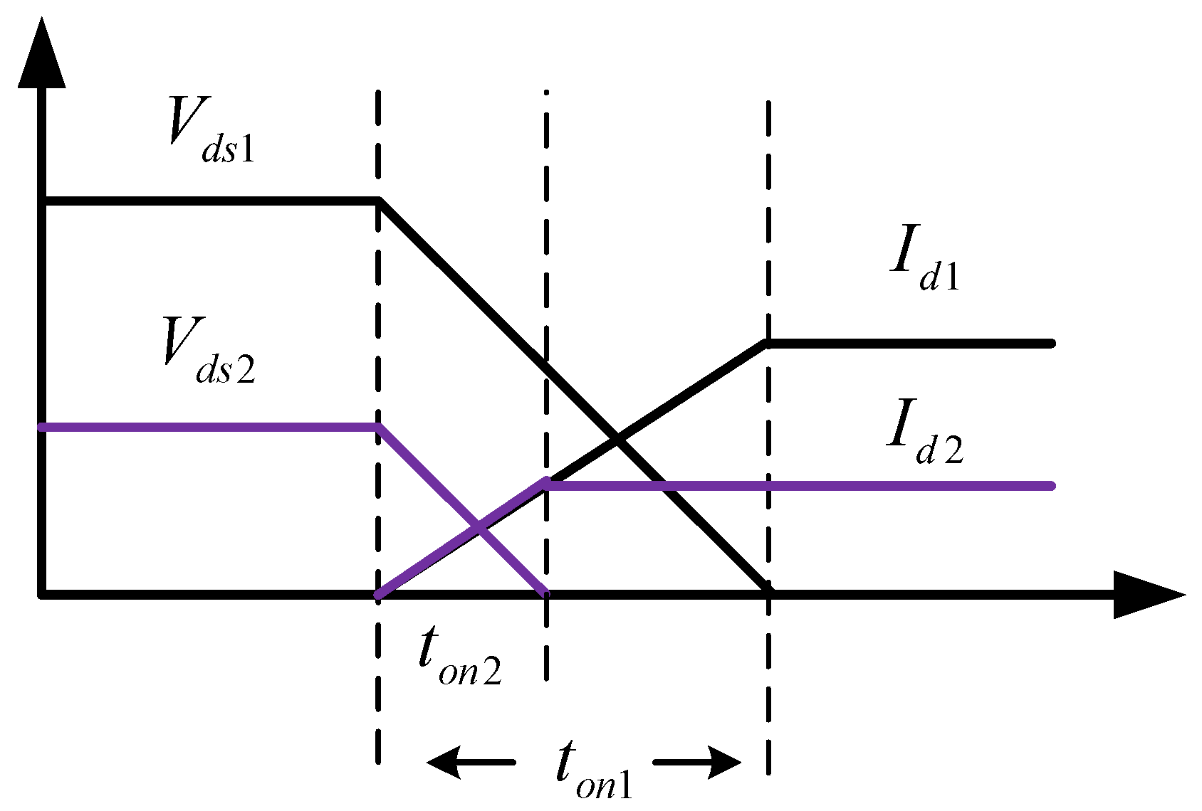
Figure 4.
Schematic diagram of full-bridge inverter.
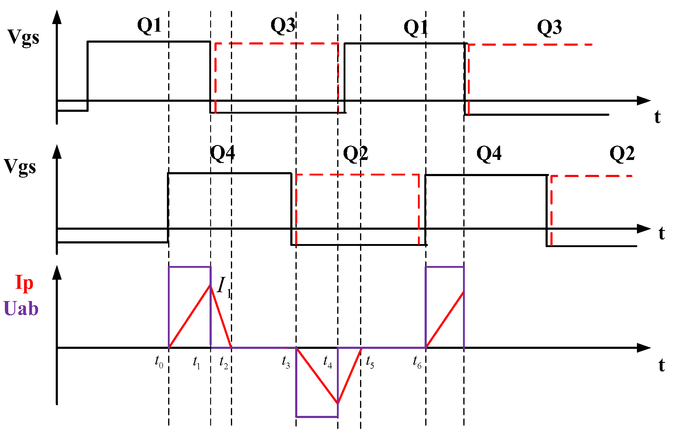
Figure 5.
The principle of SPWM.

Figure 6.
Partial partition of AC output of two-level inverter.
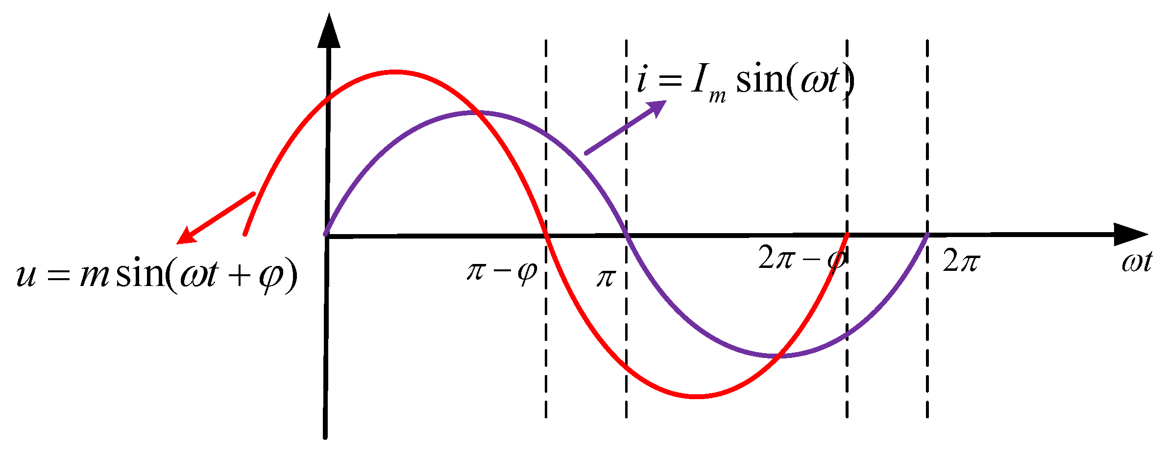
Figure 7.
V–I characteristics of SiC MOSFET and antiparallel SiC diode at different temperatures.

Figure 8.
Circuit of Double-Pulse test.

Figure 9.
Waveforms of DP test.
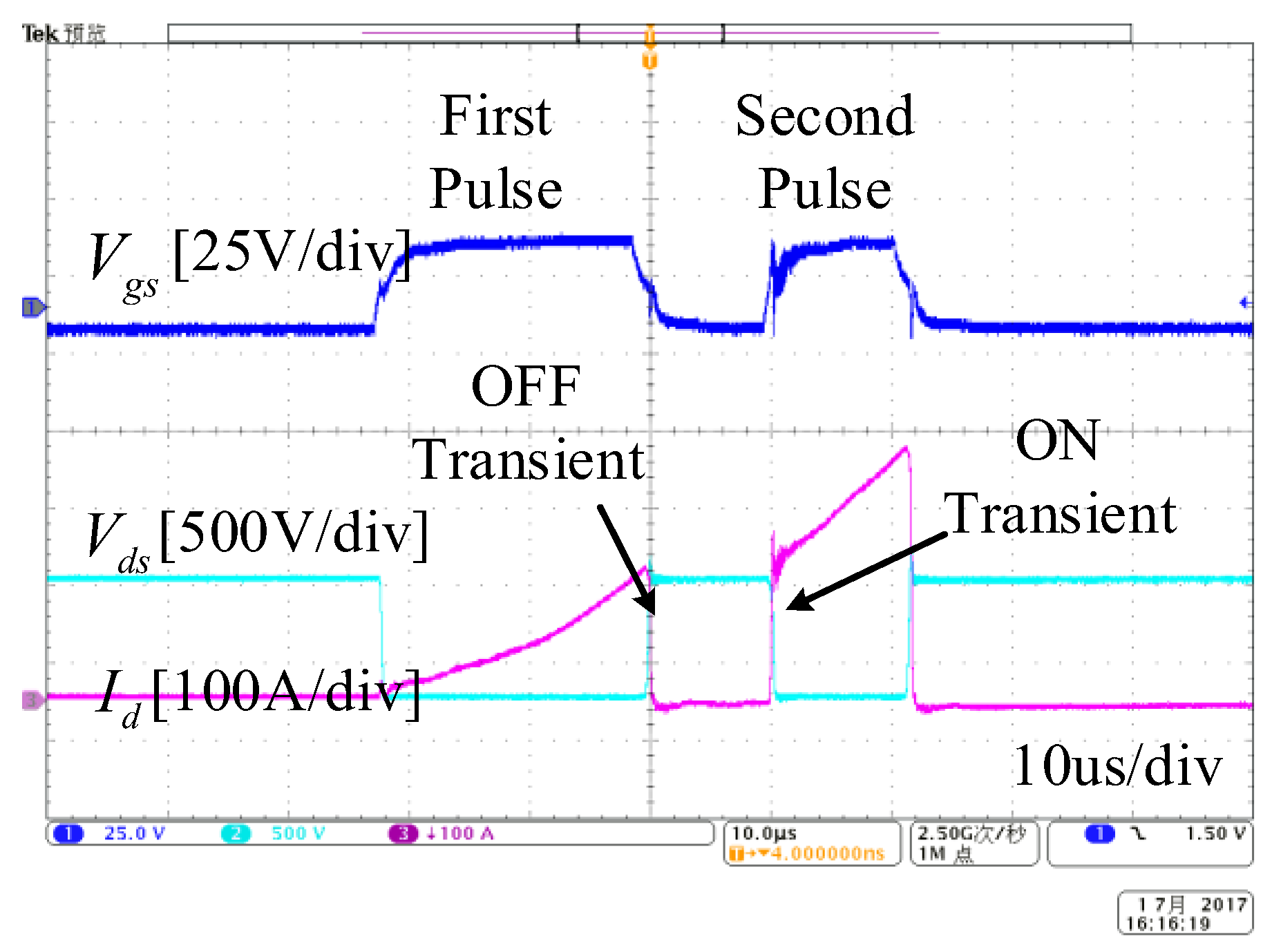
Figure 10.
Turn-on characteristics with and .

Figure 11.
Turn-off characteristics with and .
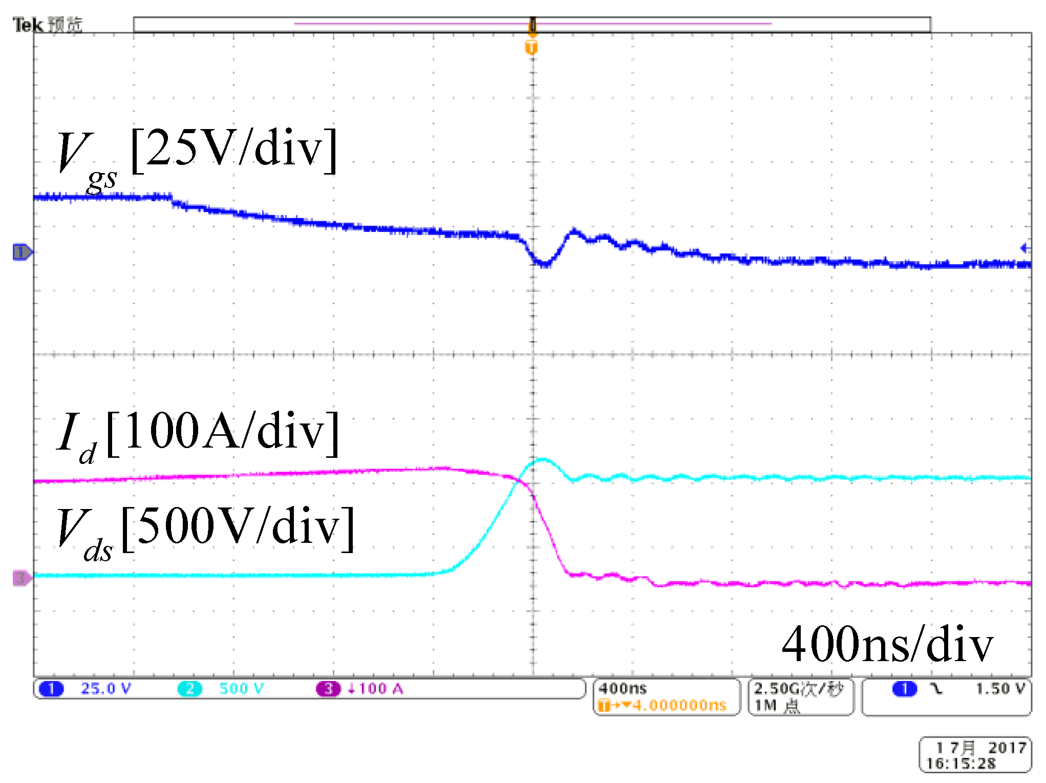
Figure 12.
and asured with and at different device currents, and different voltages, .

Figure 13.
The PLECS loss simulation model, (a) the model of the DC/DC converter, (b) the model of the three-phase inverter.
Figure 13.
The PLECS loss simulation model, (a) the model of the DC/DC converter, (b) the model of the three-phase inverter.
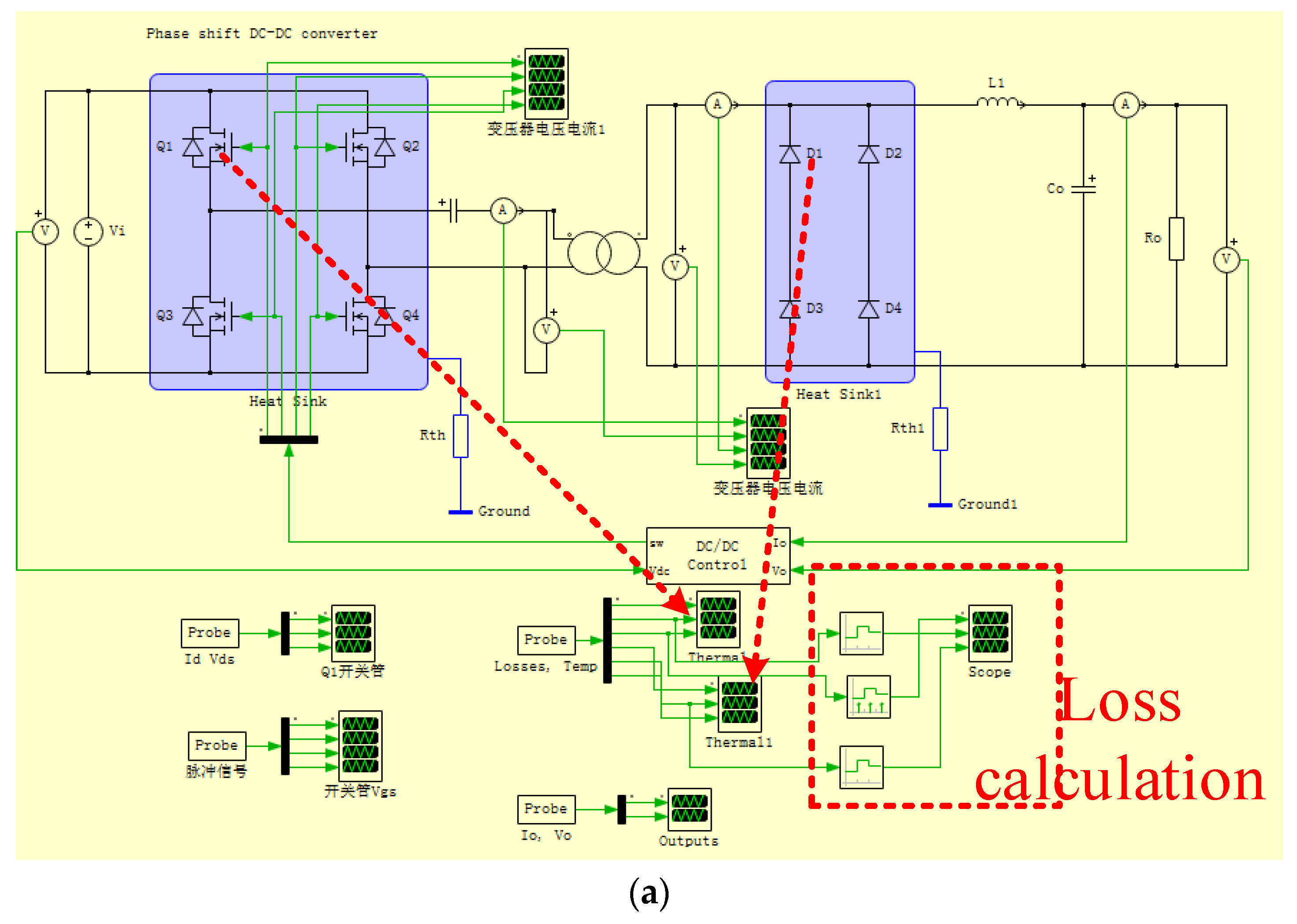

Figure 14.
The device thermal description file.
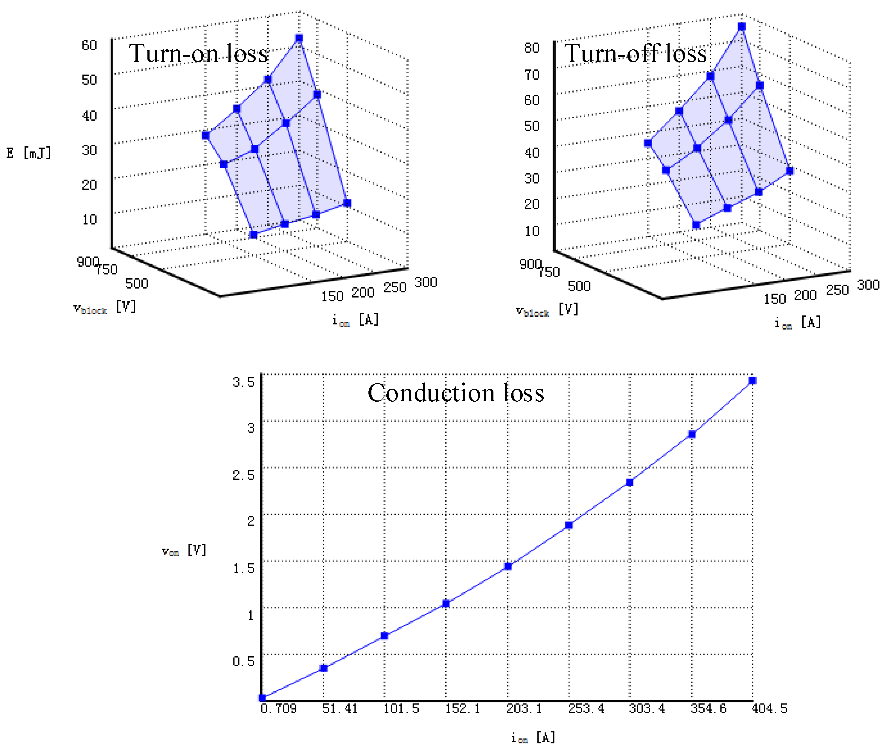
Figure 15.
The auxiliary converter.

Figure 16.
The full-bridge inverter waveform.

Figure 17.
The rectifier waveform and three-phase inverter waveform.
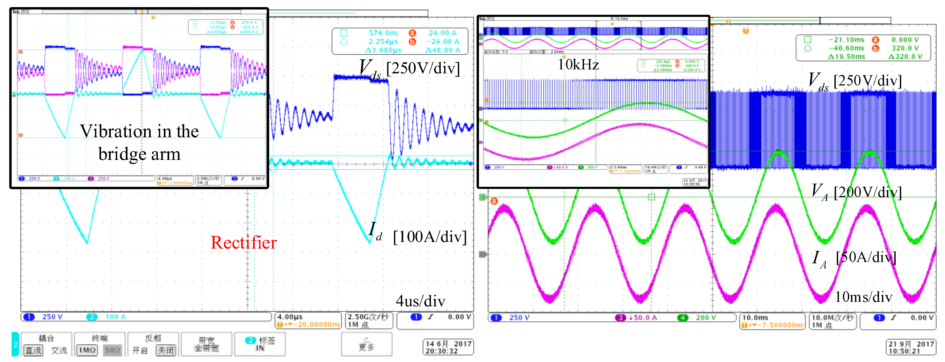
Figure 18.
Position of power measuring points.

Figure 19.
Location of the SiC device and radiator.

Figure 20.
The thermal images of three modules (a) the full bridge inverter; (b) the rectifier and the three-phase inverter.
Figure 20.
The thermal images of three modules (a) the full bridge inverter; (b) the rectifier and the three-phase inverter.

Table 1.
System parameters.
| Parameter | Value |
|---|---|
| Rated input voltage/V | DC750 |
| Rated output power/kW | 40 |
| Rated output voltage/V | AC380/3p |
| Rated output frequency/Hz | 50 |
| Input voltage of inverter/V | 650 |
| Switching frequency of DC/DC/kHz | 40 |
| Switching frequency of three-phase inverter/kHz | 10 |
| Three-phase output filter inductance/mH | 1.2 |
| Three-phase output filter capacitor/uF | 3 × 200 |
| Transformer ratio | 1:1.4 |
Table 2.
The parameters of theoretical calculation.
| Parameter | Value | Parameter | Value |
|---|---|---|---|
| 750 | 25 | ||
| 650 | 40 | ||
| 7 | 10 | ||
| 5 | 0.95 | ||
| 8 | 0.994 | ||
| 1.7 | 87 |
Table 3.
Loss comparison of simulation and theory.
| Module | Theoretical Calculation Values | Simulated Values | ||
|---|---|---|---|---|
| On-State Loss/W | Switching Loss/W | On-State Loss/W | Switching Loss/W | |
| Full-bridge inverter | 230.98 | 1926.88 | 311.6 | 1733.6 |
| Rectifier | 338.56 | - | 403.2 | - |
| Three-phase inverter | 118.32 | 92.04 | 160.8 | 117.6 |
Table 4.
Loss comparison of simulation, theory and experiment.
| Module | Theoretical Calculated Value/W | Simulated Value/W | Experimental Value/W |
|---|---|---|---|
| Full bridge inverter | 2157.86 | 2045.2 | 2144.73 |
| Rectifier | 338.56 | 403.2 | 468.89 |
| Three-phase inverter | 210.36 | 278.4 | 254.05 |
© 2017 by the authors. Licensee MDPI, Basel, Switzerland. This article is an open access article distributed under the terms and conditions of the Creative Commons Attribution (CC BY) license (http://creativecommons.org/licenses/by/4.0/).
Share and Cite
MDPI and ACS Style
Liu, H.; Huang, X.; Lin, F.; Yang, Z. Loss Model and Efficiency Analysis of Tram Auxiliary Converter Based on a SiC Device. Energies 2017, 10, 2018. https://doi.org/10.3390/en10122018
AMA Style
Liu H, Huang X, Lin F, Yang Z. Loss Model and Efficiency Analysis of Tram Auxiliary Converter Based on a SiC Device. Energies. 2017; 10(12):2018. https://doi.org/10.3390/en10122018
Chicago/Turabian StyleLiu, Hao, Xianjin Huang, Fei Lin, and Zhongping Yang. 2017. "Loss Model and Efficiency Analysis of Tram Auxiliary Converter Based on a SiC Device" Energies 10, no. 12: 2018. https://doi.org/10.3390/en10122018
Note that from the first issue of 2016, this journal uses article numbers instead of page numbers. See further details here.