Article

Evaluation and Reliability Assessment of GaN-on-Si MIS-HEMT for Power Switching Applications

1
Department of Mechanical Engineering, National Chiao-Tung University, No. 1001, University Road, Hsinchu 30010, Taiwan
2
Department of Materials Science and Engineering, National Chiao-Tung University, No. 1001, University Road, Hsinchu 30010, Taiwan
3
Microsystems Technology Laboratories, Massachusetts Institute of Technology, Cambridge, MA 02139, USA
*
Author to whom correspondence should be addressed.
Energies 2017, 10(2), 233; https://doi.org/10.3390/en10020233
Submission received: 6 December 2016 / Revised: 20 January 2017 / Accepted: 8 February 2017 / Published: 16 February 2017
(This article belongs to the Special Issue Semiconductor Power Devices)

Abstract

:
This paper reports an extensive analysis of the physical mechanisms responsible for the failure of GaN-based metal–insulator–semiconductor (MIS) high electron mobility transistors (HEMTs). When stressed under high applied electric fields, the traps at the dielectric/III-N barrier interface and inside the III-N barrier cause an increase in dynamic on-resistance and a shift of threshold voltage, which might affect the long term stability of these devices. More detailed investigations are needed to identify epitaxy- or process-related degradation mechanisms and to understand their impact on electrical properties. The present paper proposes a suitable methodology to characterize the degradation and failure mechanisms of GaN MIS-HEMTs subjected to stress under various off-state conditions. There are three major stress conditions that include: VDS = 0 V, off, and off (cascode-connection) states. Changes of direct current (DC) figures of merit in voltage step-stress experiments are measured, statistics are studied, and correlations are investigated. Hot electron stress produces permanent change which can be attributed to charge trapping phenomena and the generation of deep levels or interface states. The simultaneous generation of interface (and/or bulk) and buffer traps can account for the observed degradation modes and mechanisms. These findings provide several critical characteristics to evaluate the electrical reliability of GaN MIS-HEMTs which are borne out by step-stress experiments.

1. Introduction

AlGaN/GaN high electron mobility transistors (HEMTs) have attracted a lot of attention for both switching and radio frequency (RF) power applications [1,2,3]. The Schottky-gate-controlled heterojunction two-dimensional electron gas (2DEG) channel, which is widely used for high-frequency RF applications [4] is not desirable for next generation power electronics for the following reasons. Firstly, HEMTs are struggling to achieve high breakdown voltage, low on-state resistance and fast switching at the same time. Since the Schottky barrier layer suffers from possible damage in the subsequent processing steps, the large gate leakage current increases the off-state loss and reduces power supply efficiency [5,6]. Secondly, the 2DEG of conventional HEMT structures cannot be easily depleted under the gate for normally-off (E-mode) operation [7,8]. E-mode field-effect transistors (FETs) are essential in power electronics applications for avoiding circuit burnout and realizing great simplicity in circuit design. Finally, the long-term stability and reliability of the Schottky gate HEMT remains problematic. If the devices are stressed for a sufficiently long time, the gate leakage current increases and becomes noisy, and degradation occurs even below the critical voltage [9,10,11,12].
Different approaches are proposed to reduce the gate-leakage current and enlarge the gate voltage swing. One straightforward solution is to insert a dielectric layer between the gate metal and the AlGaN layer to block the leakage current path [13,14]. The frequently-used dielectrics are Al2O3 and Si3N4, due to the large band gap and high breakdown field, and the ability to deposit high quality films by ALD (Atomic Layer Deposition), plasma enhanced CVD (PECVD) or other conventional means. However, several studies report that the Al2O3/nitride heterogeneous interface contains a high density of deep states that result in threshold voltage hysteresis when the transistor is used as a switching device [15,16]. For this reason, source-side breakdown mechanism in metal-insulator-semiconductor (MIS)-HEMTs is an important reliability concern [17,18]. The Si3N4 film could be a promising alternative candidate as a gate dielectric for GaN power MIS-HEMTs. Si3N4-based MIS devices can be both D-mode and E-mode. The challenge of making E-mode transistors is to maintain low on-resistance (Ron) with a large gate swing. D-mode MIS devices are widely used for power electronics applications in a cascode configuration with a low voltage Si-based metal-oxide-semiconductor field-effect transistor (MOSFET) in series [19,20,21]. Compared to the conventional HEMT structure with Schottky-gate, relatively few studies on the degradation of HEMT structure with MIS-gate are presented in the literature [22,23,24]. More detailed investigations are needed to identify symptoms of different degradation mechanisms and to understand how it impacts the device’s electrical characterization in detail.
A method to evaluating device reliability through the short-term step-stress measurements of several figures of merit (IDMAX, IGOFF, RD, RS and Vth) was proposed for Schottky-gate HEMTs [25]. The voltage at which significant electrical degradation takes place is called the critical voltage (VCRI) [26,27]. Within this context, the aim of this paper is to contribute to the understanding of device early failures and associated structural degradation for power electronic device designers. The impact of short-term step-stress on gate leakage current (IGoff), stress gate current (IG_stress), device on-resistance (Ron), and threshold voltage (Vth) are measured, statistics are studied, and correlations are investigated under several different off-state conditions.
A flow chart of a typical step-stress test is shown in Figure 1. The analysis is carried out in an on-wafer probe station equipped with thermal chuck that allows device characterization through external test equipment (two Keithley 2636B SourceMeters). The devices are kept for a long time under the different off-state stress conditions at a base plate temperature Tbase (25 °C); in each stage, the variation in DC figures of merit (Table 1) are evaluated by switching the devices to the ON-state by means of short voltage pulses. The quick characterization techniques are used to acquire a complete description of the degradation process. Self-heating effects are not taken into account in the measurements due to the off-state stress where there should be negligible current flow and heating. In the first set of conditions, the gate-to-source voltage (|VGS|) is increased at a constant drain-to-source voltage (VDS) of 0 V; a harsh stress condition relative to the targeted normal conditions for these GaN MIS devices. The second set of experiments involves the step stressing of VDS with VGS biased at −20 V (off-state condition). Furthermore, the source terminal of the GaN based cascode switch is connected to the gate terminal of the D-mode MIS GaN transistor, so the voltage difference should be 0 V. In contrast to the large number of papers reporting on issues for a GaN HEMT under off-state VDG stress, there are few publications focusing on reliability issues for the GaN cascode switch under off-state stress (with the gate shorted to ground) for long periods of time. In the third experiment, the source-to-gate voltage (VSG) is increased at a constant drain-to-gate voltage (VDG) of 20 V (off-state condition). Furthermore, 3-terminals I-V characterization techniques are also employed to identify degradation mechanism in the heterostructure.
This present paper proposes a methodology for the analysis of failure modes and mechanisms of GaN MIS HEMTs. A series of step-stress experiments are performed to investigate the degradation mechanism of D-mode MIS-HEMTs.

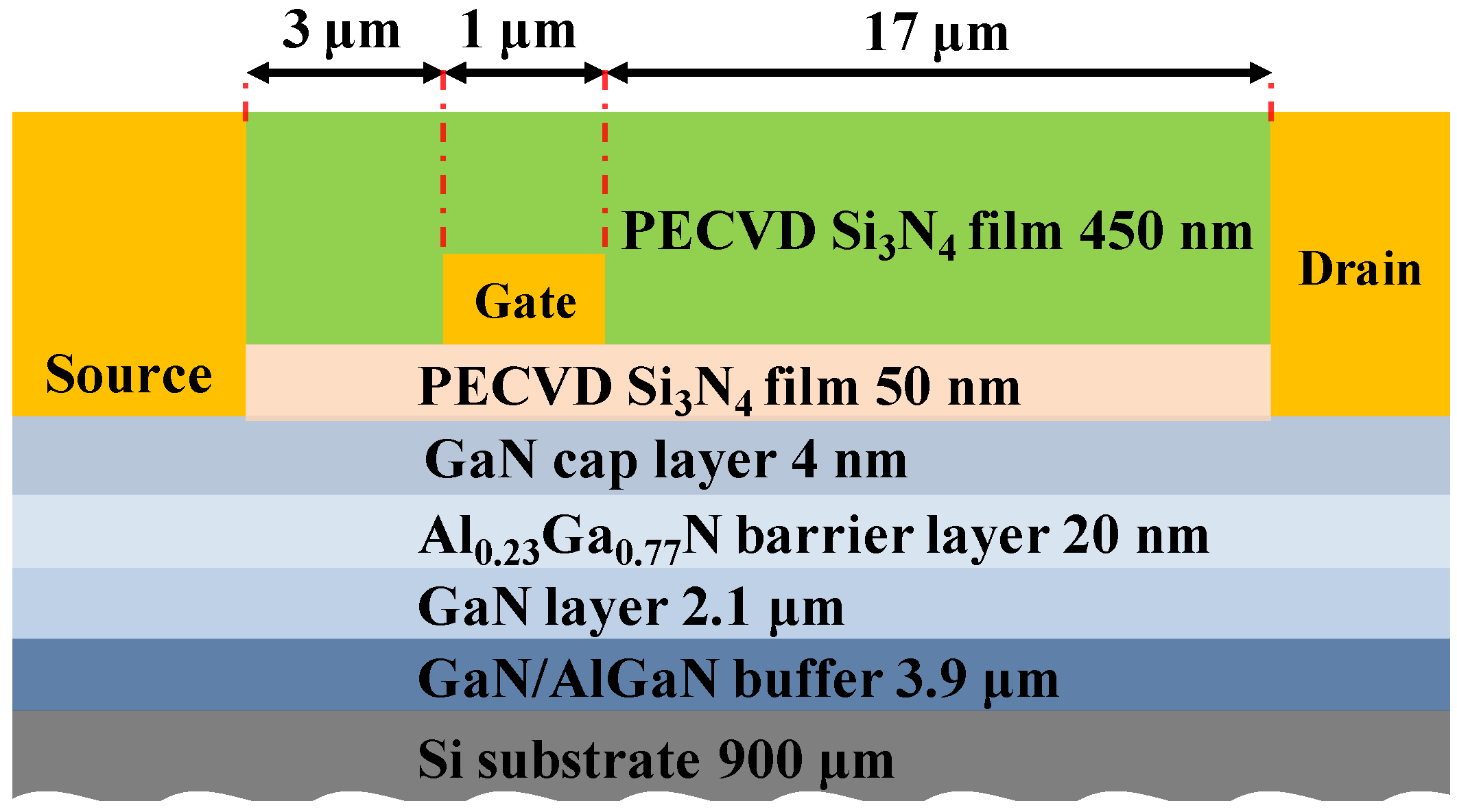
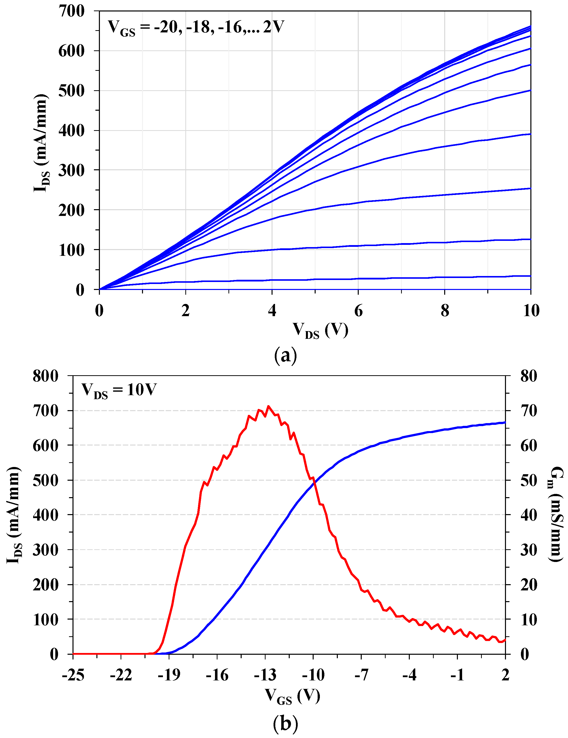
2. Device Structure and Experimental Setup

A schematic of the AlGaN/GaN MIS-HEMT is shown in Figure 2. This device was fabricated using a complete complementary metal oxide semiconductor (CMOS)-compatible process for GaN-based MIS-HEMTs on Silicon. The AlGaN/GaN heterostructure epilayer was grown on a silicon substrate (thickness, 900 μm) by metalorganic chemical vapour deposition (MOCVD). The epitaxial structure consisted of a 3.9 μm-thick GaN/AlGaN buffer layer, on which was deposited a 2.1 μm-thick GaN layer, a 20 nm-thick Al0.23Ga0.77N barrier layer and, finally, a 4 nm-thick GaN capping layer.
To fabricate this device, Mesa isolation was performed with an ICP-RIE system with Cl2 as the etching gas. Source/drain Ohmic contacts were formed with e-beam evaporation and lift-off of Ti/Al/Ni/Au (20 nm/120 nm/25 nm/100 nm) metal stack, followed by rapid thermal annealing at 800 °C in N2 for 60 s. After removing the photoresist and carrying out a surface cleaning process to remove impurities and reduce surface dangling bonds, a 50 nm-thick Si3N4 film was immediately grown by plasma-enhanced chemical vapor deposition (PECVD) and deployed as the gate insulator. The gate electrode was formed with Ni/Au (50 nm/450 nm) deposited upon the top of the dielectric stack. Finally, the device was covered with a 450 nm-thick PECVD Si3N4 film. The device geometry consists of LGD = 16 μm, LGS = 3 μm, gate length = 1 μm and gate width = 50 μm. Before starting with the step-stress experiments, the various static characteristics (Figure 3) such as IDS-VDS, IDS-VGS, Gm-VGS, and leakage current for both the devices were evaluated and sorted to obtain well matched degradation characteristics; we verified that devices belonging to the same wafer presented consistent and reproducible behavior. The devices belonging to the center region of a wafer were cut out and divided into three groups (n = 10/group) for this study; a total of approximately 40 devices were tested [28].
The devices are mounted on AlN substrate (180 W/m∙K) to ensure that no electrons diffuse into channels. All the experiments are performed in a probe station with a thermally controlled stage, and Fluorinert™ (FC-40) is applied on the device surface to avoid arcing and water-assisted electrochemical reactions caused by environmental conditions. For devices that are soldered into the substrate, a thin attachment layer of sintered nano-silver is applied to the bottom of the substrate to ensure that the least amount of contact resistance exists between the substrate and the lead-frame. Thermal grease is also used at the interface between the ceramic-attached lead-frame and the stage.
This study focuses on the impact of gate leakage current in reverse bias IGoff, the degradation of the on-resistance Ron, the bias gate current IG_stress obtained at the 29th second (step-stress on gate and source) or 179th second (step-stress on drain) for each stress cycle, and the shift in threshold voltage Vth. However, the degradation in IDmax is found to be recoverable and related to thermally-assisted electron de-trapping. This has been suggested to be resulting from the device reaching a new steady-state as trapping and de-trapping reach equilibrium. Using step-stress methods of the terminals of gate, drain and source terminal; a detailed study is performed to observe device degradation that limits safe operation in the off-state.

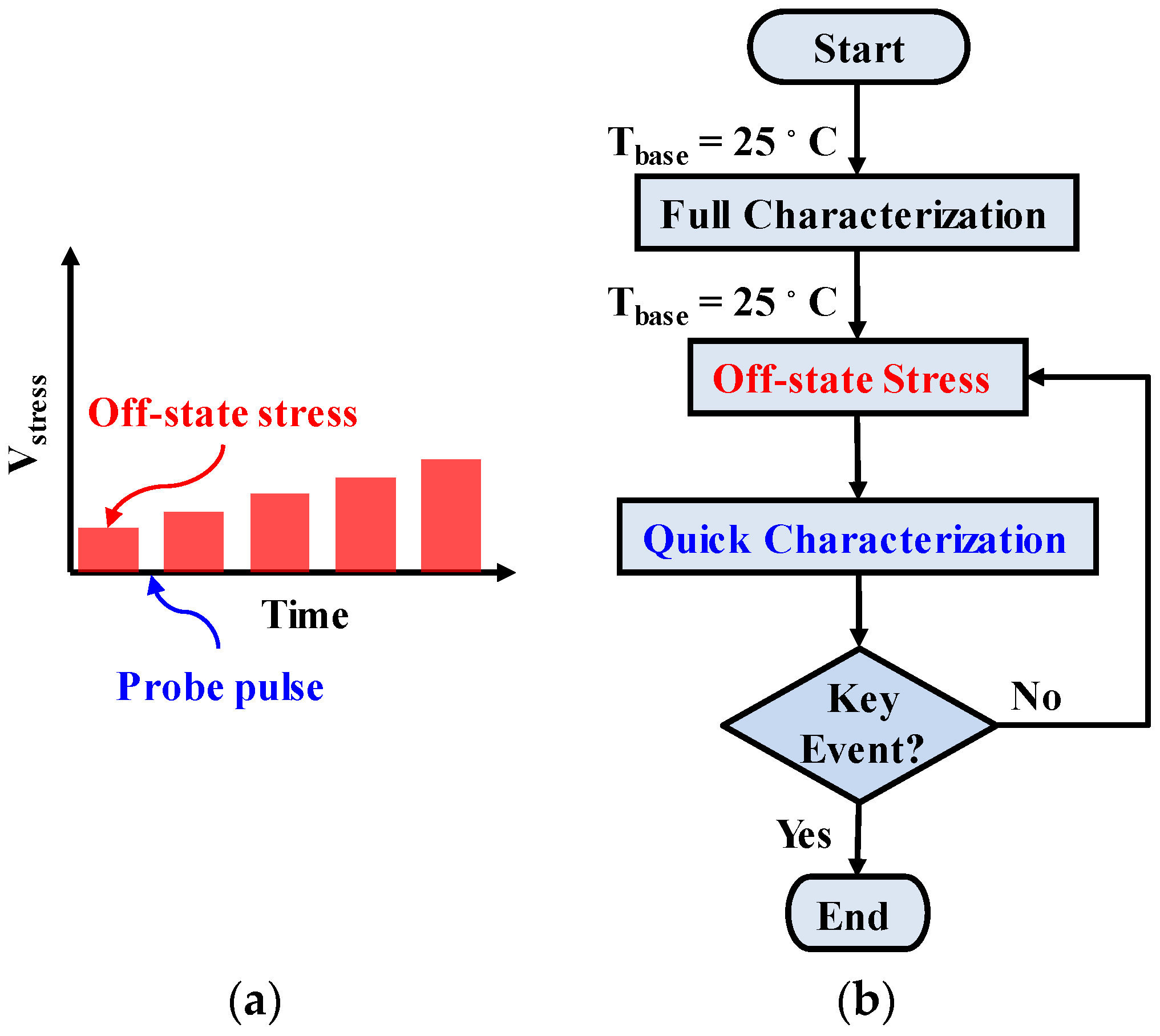
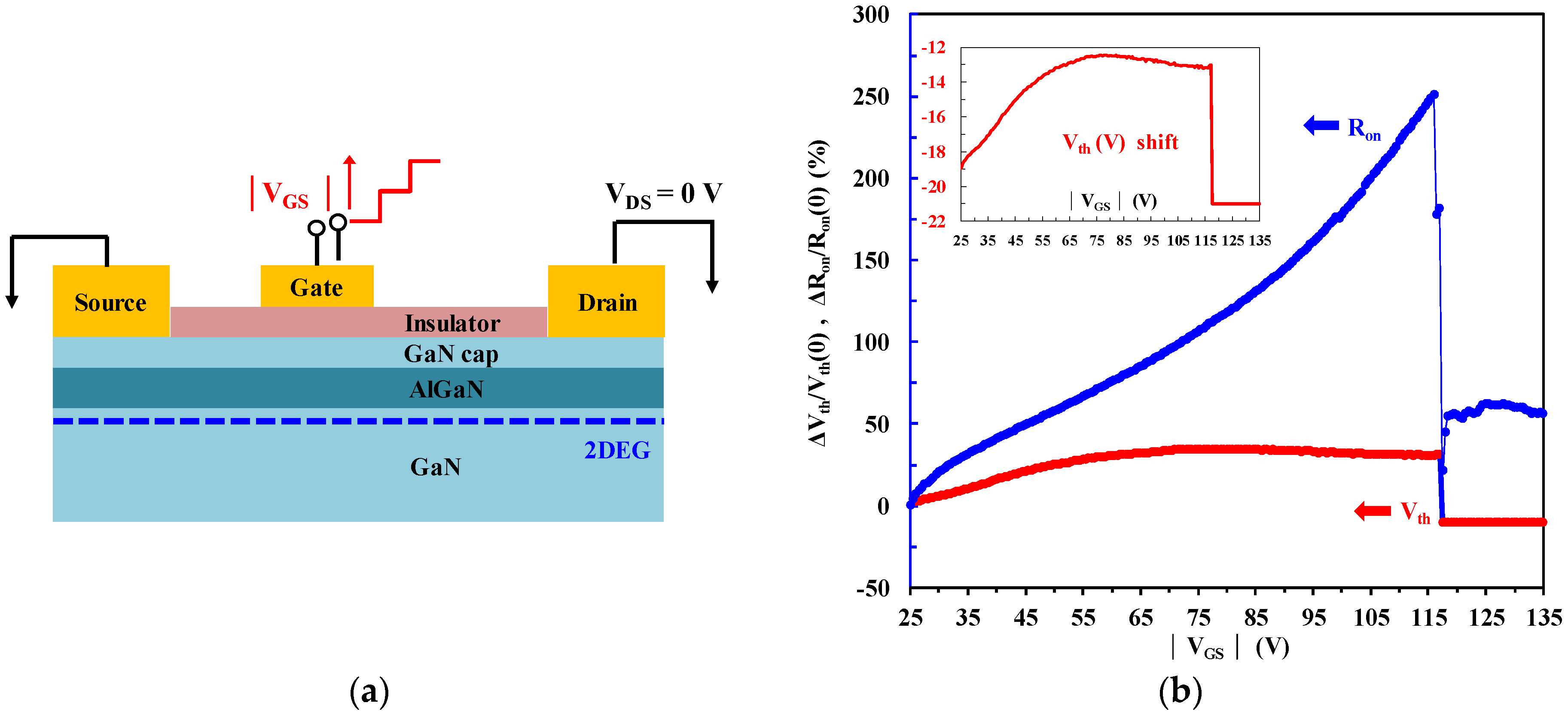
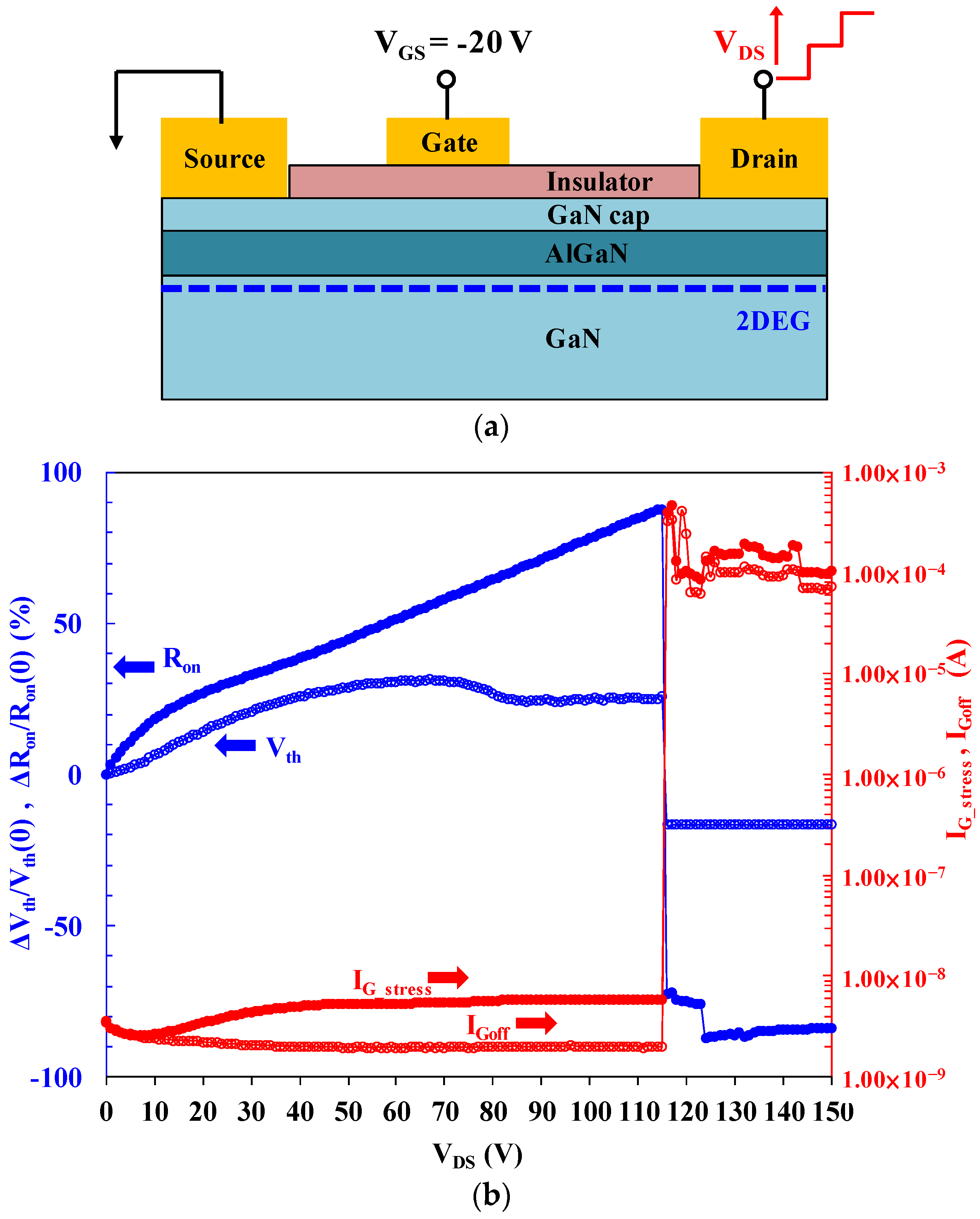
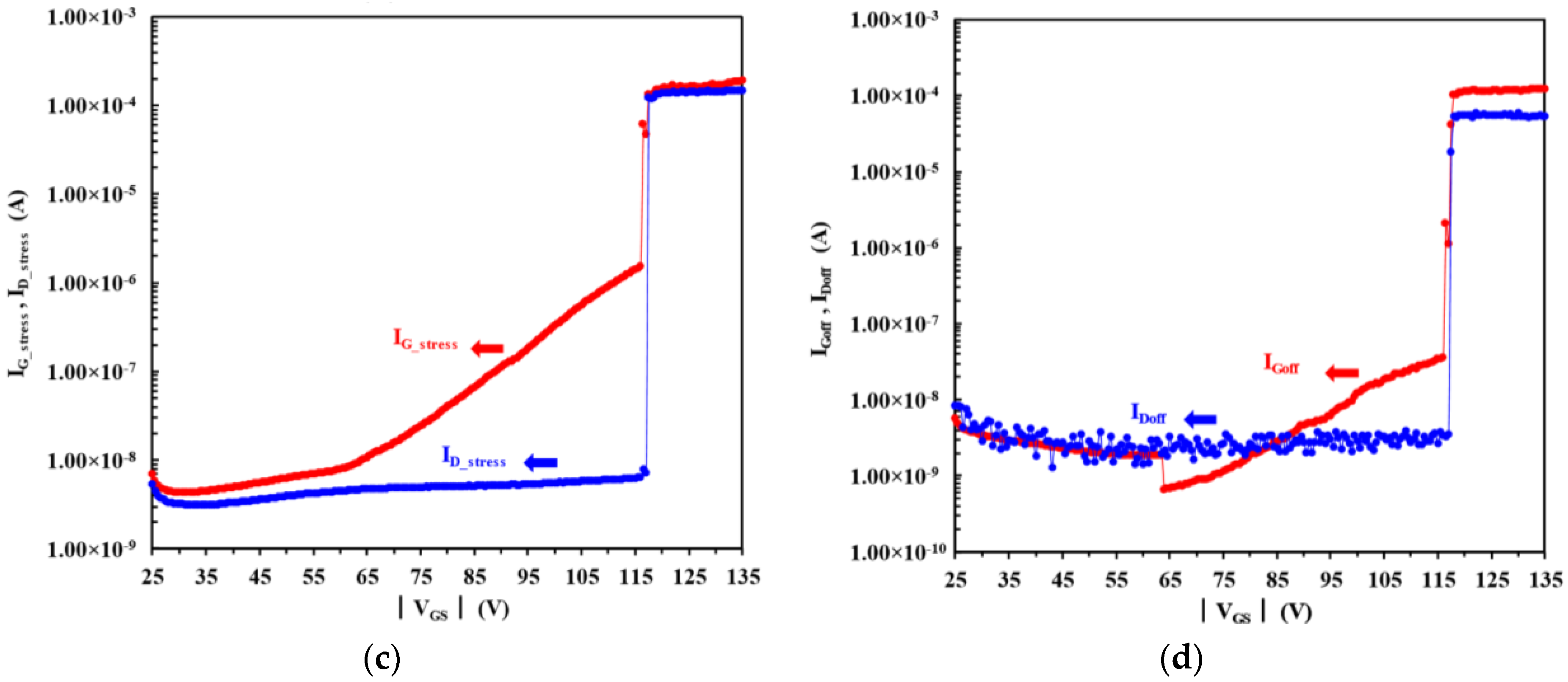
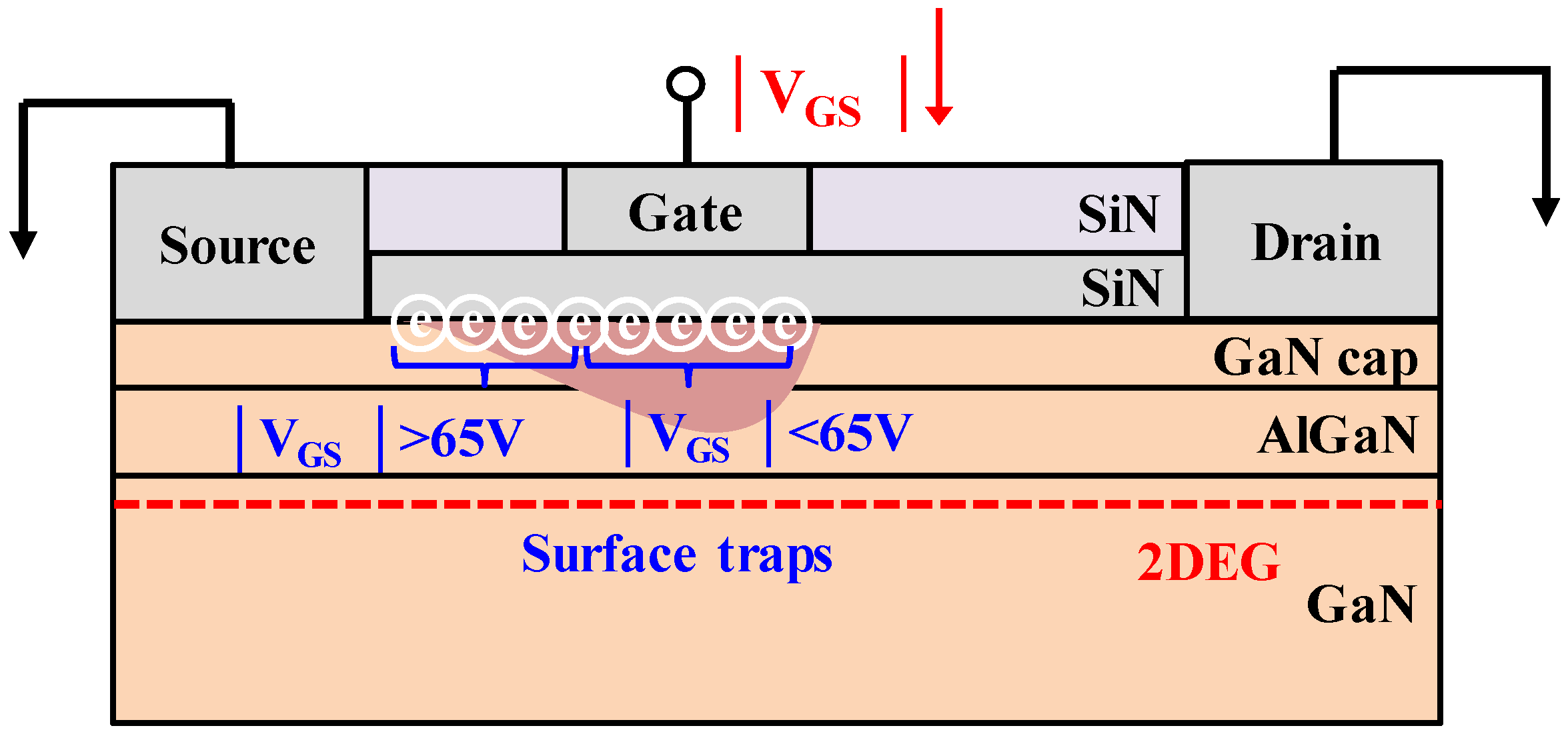
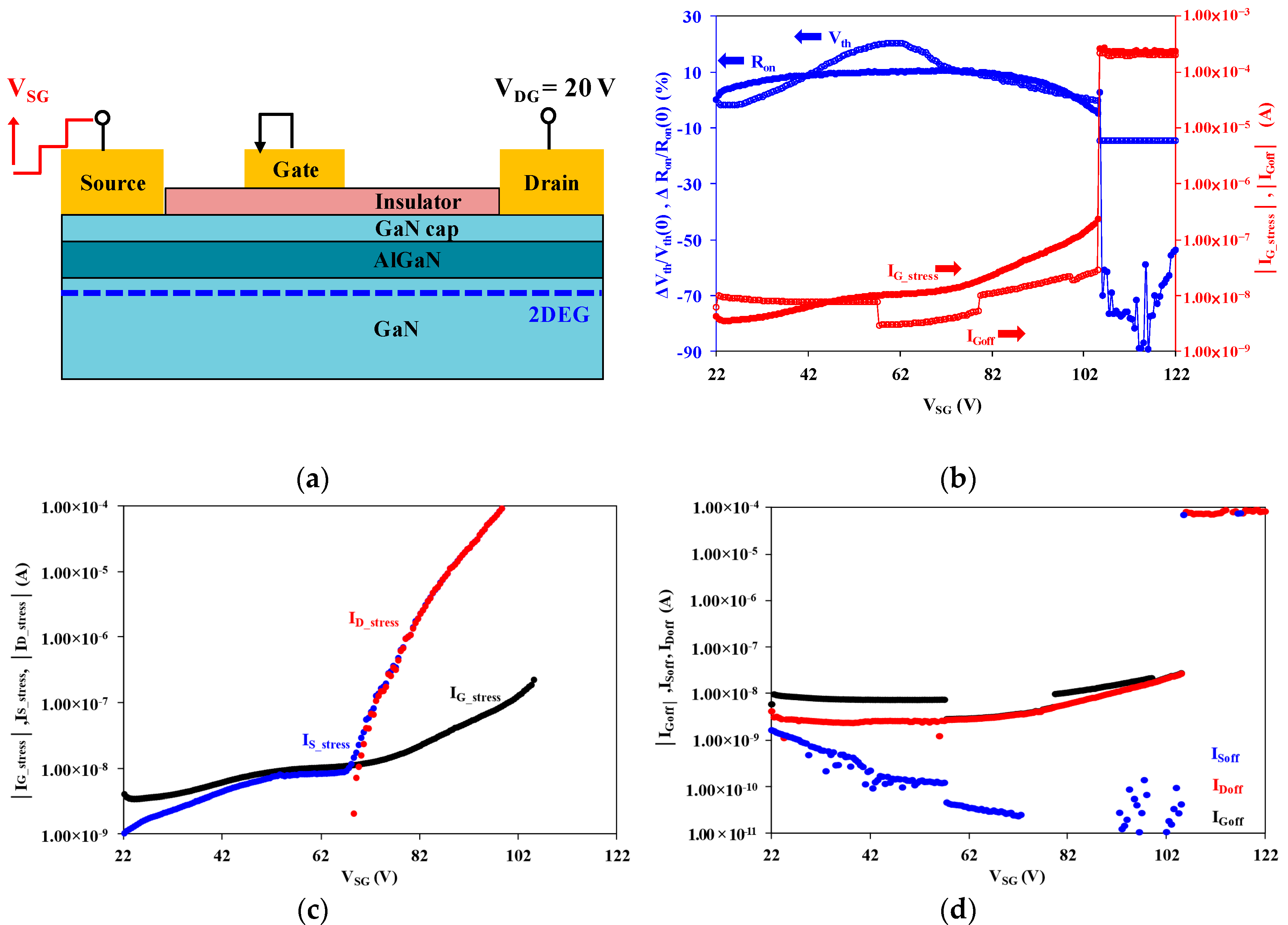
3. Short-Term Step-Stress Experiment

Under high reverse gate bias conditions, crystallographic defects and even cracking occur as a result of the inverse piezoelectric effect [29,30]. The presence of a strong electric field in the piezoelectric GaN and AlGaN leads to additional mechanical stress that is concentrated at the gate edge across the AlGaN barrier [31]. The change in AlGaN elastic energy can produce dislocations (extended defects). By inserting an insulator under the gate metal such as ALD Al2O3 and PECVD Si3N4, MIS-gate HEMTs are highly preferred over Schottky-gate HEMTs for high-voltage power switches. The MIS-gate structure is effective for suppressing the gate leakage current and thus improving long-term reliability. However, this MIS-gate technology still remains challenging in terms of obtaining low and stable gate leakage characteristics and achieving sufficient long-term robustness simultaneously.
To study the impact of negative gate-bias (VGS) stress on the performance of Si3N4 gate dielectric, the device is step-stressed at VDS = 0 V (shorted source and drain) with increasing values of |VGS| from 25 V to 135 V for harsh bias condition, as shown in Figure 4a. At each step, the device is stressed for 30 s. Since the voltage across the drain and source is constant throughout the experiment, both the drain and source sides of the gate are stressed with increasing electric fields over time.
Figure 4b–d shows a positive shift in threshold voltage Vth (up to 30%), a corresponding increase in dynamic Ron (up to 200%), and an increase in gate current (IG_stress, and IGoff) observed in a representative sample during the step-stress experiment with VDS = 0 V. Starting with the step at 116 V, a sudden increase in IG_stress is observed, as well as a permanent increase in both gate currents several orders of magnitude at the end of the 118 V step (burnout failure). Gate current (IG_stress) first increases, following the increase in IGoff, and then increases due to the creation of gate-edge degradation. In an experiment of this kind, the evolution of IGoff during stress reveals that for low values of |VGS|, IGoff tends to drop with a given stress step. This can be attributed to trapping associated with defects at the gate edges, where the electric field is highest [32]. The defects promote the injection of electrons from the gate into the Si3N4 insulating layer and at the Si3N4/GaN interface. In the degraded device where localized vertical leakage paths exist under the gate electrode, a significant number of electrons is injected from the gate electrode to the Si3N4 insulating layer and the insulating layer is eventually driven into breakdown (from |VGS| = 65 V), due to tunneling and subsequent trapping within the dielectric over layer.
It is interesting to see evidence of stress-induced gate current (IG_stress and IGoff) at high gate voltage and a critical gate voltage (|VGS| = 65 V) beyond which IGoff degrades suddenly. Figure 5 shows the trapping and degradation mechanisms in GaN-Based MIS-HEMTs [33]. The injection of electrons towards the AlGaN layer under the gate electrode induces an increase in Ron and a positive shift in threshold voltage Vth until the critical voltage is reached. The accumulation of negative charge in the AlGaN layer forms a virtual gate that depletes part of the channel. During the stress period (from |VGS|= 25 to 65 V), ∆Vth increases with |VGS| and eventually saturates. Stressing beyond the critical gate voltage creates interface traps at the SiN/AlGaN interface in the gate-source access region, while no significant changes are observed for both drain currents (IDoff and ID_stres), as shown in Figure 4c,d. The injection of electrons induces an increase in Ron and no obvious change in threshold voltage Vth. These traps become a pathway for electrons to flow from the gate to the source. During stress, when electrons refill the interface traps, both IGoff and IG_stress sharply increase. This indicated that the traps are mainly located at the SiN/AlGaN interface.
Also of interest is the fact that IG_stress exhibits different degradation behavior before and after biasing to the critical gate voltage. To verify the origin of the observed degradation caused by high electric field, two possible off-state failure mechanisms are investigated. One is a vertical injection of electrons from the gate into the Si3N4 insulating layer, due to trap assisted tunneling, and the other is a lateral component, also due to tunneling, which involves injecting electrons directly into trap states at the SiN/AlGaN interface. The injection of electrons from the gate electrode into interface states present in the gate-source region extends laterally toward the source contact with increasing gate voltage. Degradation is detected as a non-recoverable increase in the gate current (step at |VGS| = 116 V and beyond). These results also indicated that electrons injected into surface states near the gate terminal form an extended virtual gate near the gate terminal edge extending the depletion region of the device channel. This is consistent with the positive Vth shift and corresponding increase in Ron.
Figure 6a shows the off-state step-stress experiments carried out under normal use conditions. Identical devices are also step-stressed at VGS = −20 V (off-state) with increasing values of VDS from 1 to 150 V, with a step size of 1 V (3 min at each step). To obtain enough degradation for a reasonable analysis of device reliability, limited by the instrument’s capabilities (voltage rating 200 V), accelerated life testing involves applying the VDS bias stress for an extended period of time (3 min). In this approach, the voltage across the gate and source (VGS) is constant throughout the experiment and a high electric field peak appears at the drain side edge of the gate with the field penetrating deeply into the buffer.
Referring to Figure 6b, significant degradation takes place in Vth and Ron while a minor increase in IG_stress is observed until the applied bias voltage (VDS) exceeds 114 V. As the drain bias voltage (VDS) increases, a significant increase of Vth and RON indicates that the applied electric field increases the probability for the trapped electrons both at the surface (high electric field between gate and drain) and in the buffer (high vertical field from the drain directed towards the substrate); these trap effects are due to the increased injection of electrons from the gate electrode toward the gate–drain surface (lateral trapping) and from the substrate to the buffer (vertical trapping) simultaneously [34]. In-situ passivation combined with buffer optimization is a necessary step toward the reduction of off-state stress-induced change in Vth and RON ratio. There is a significant degradation up to around VDS = 114 V. At this critical degradation voltage, change in all figures of merit starts sharply and degradation increases as the stress experiment proceeds. Similar to a degradation mechanism in traditional Schottky gate HEMTs, a sharp increase of IG_stress and IGoff at a certain voltage has been observed in MIS-HEMTs.
The previous measurements were carried out starting from a negative gate voltage or from a high VDG quiescent point; thus, it is possible to induce strong trapping both under the gate and in the gate-drain access region, observing the onset of electric field-induced degradation of selected DC figures of merit. Also of interest is the behavior of the GaN cascoded structure which needs to be considered during the high current turn-off condition. With this configuration, the gate-to-source voltage of GaN MIS-HEMT is equal to the source-to-drain voltage of Si MOSFET. The interaction between the two discrete devices (Si MOSFET and GaN MIS-HEMT) may result in instability due to the unavoidable package parasitic inductance. The package influence during high current turn-off could be a significant internal parasitic ringing which may cause GaN device failure [35]. The gate isolation barrier of GaN MIS-HEMT will usually break before Si MOSFET reaches avalanche. This leads to an immediate damage of the GaN cascode. Considering the dynamic avalanche generation, the gate isolation barrier will easily break due to high voltage peaks on the GaN source-gate access region. The issue of avalanche robustness deserves special mention.
In this work, a novel step-stress methodology is presented to study the potential failure mode of the cascode GaN device as shown in Figure 7a. To show that the gate degradation occurs solely in regions with high electric field, the devices are stressed by reversing the source/drain terminals. The gate terminal is grounded in this configuration. In this experiment, the VSG is stepped in 0.5 V increments for 30 s per step from 22 V to 122 V while keeping VDG = 20 V under pinched-off condition. In Figure 7b, failure occurred at a low voltage of 105 V. MIS devices are functional throughout the stress. At VSG = 105 V, the IG_stress and IGoff suddenly increase and Vth rapidly becomes more negative causing the device to turn-on. The Vth shift changes from positive to negative direction with off-state stress beyond a certain critical voltage of VSG = 63 V.
Figure 7c shows the degradation evolution of 3-terminal I–V characteristics of ID_stress, IG_stress, and IS_stress during this stress experiment. It is interesting to show that both ID_stress and IS_stress exhibit a sharp rise around the same critical voltage denoted in Figure 7b, while IG_stress presents a negligible change. This phenomenon implies that degradation takes place at dielectric/III-N barrier interface in the access region between the gate and source. Furthermore, 3-terminal I–V characteristics (IDoff, IGoff, and ISoff), described in Figure 7d, show negligible change, which suggest SiN/AlGaN interface state generation early in the stress experiment in addition to electron trapping in the SiN passivation or the AlGaN barrier. The findings may explain by potential failure modes of the cascode GaN-based switch from internal parasitic ringing under hard-switching turn-off condition. Short-term stress is enough to produce significant structural degradation if the stress voltage (VSG) is higher than the critical voltage (VCRI). This reliability issue needs to be taken into consideration while D-mode MIS HEMTs are used in cascode-switch application.

4. Conclusions

Leakage-current reduction and breakdown voltage increase in GaN HEMTs are achieved by the incorporation of a suitable SiN gate dielectric layer. This paper reports on an extensive analysis of the reliability of experimental MIS-HEMTs submitted to off-state stress. A synchronized stress-characterization technique has been developed to investigate the degradation modes and mechanisms under three off-state quiescent voltage stress conditions. Results provide information on the origin of the changes in key figures of merit occurring during stress time and on the critical stress voltage for the onset of prominent degradation, which is ascribed to a defect percolation process. The step-stress strategies provide some valuable insights for future design optimization of both depletion-mode and cascode configuration GaN-based power switches. A comprehensive investigation on the origin and underlying physical mechanisms of bulk and interface traps needs to be further carried out.

Acknowledgments

This work was supported by the National Chung-Shan Institute of Science & Technology, Taiwan, under Grant No. NCSIST-103-V312 (106). The authors would like to thank Compound Semiconductor Device Laboratory of National Chiao Tung University for their technical support on AlGaN/GaN MISHEMTs devices.

Author Contributions

Stone Cheng and Po-Chien Chou conceived and designed the experiments; Ting-En Hsieh performed the experiments and analyzed the data; Po-Chien Chou and Szu-Hao Chen developed analytical tools and analyzed the data; Po-Chien Chou and Stone Cheng discussed the results, wrote the paper, and revised the manuscript at all stages; Jesús A. del Alamo provided original concept advice, and commented on the manuscript; Edward Yi Chang contributed materials and devices, and supervised the project.

Conflicts of Interest

The authors declare no conflict of interest.

References

  1. Baliga, B.J. Gallium nitride devices for power electronic applications. Semicond. Sci. Technol. 2013, 28, 074011. [Google Scholar] [CrossRef]
  2. Mitova, R.; Ghosh, R.; Mhaskar, U.; Klikic, D.; Miao-Xin, W.; Dentella, A. Investigations of 600-V GaN HEMT and GaN diode for power converter applications. IEEE Trans. Power Electron. 2014, 29, 2441–2452. [Google Scholar] [CrossRef]
  3. Mishra, U.K.; Shen, L.; Kazior, T.E.; Wu, Y. GaN-Based RF Power Devices and Amplifiers. Proc. IEEE 2008, 96, 287–305. [Google Scholar] [CrossRef]
  4. Endoh, A.; Yamashita, Y.; Ikeda, K.; Higashiwaki, M.; Hikosaka, K.; Matsui, T.; Hiyamizu, S.; Mimura, T. Non-Recessed-Gate enhancement-mode AlGaN/GaN high electron mobility transistors with high RF performance. Jpn. J. Appl. Phys. 2004, 43, 2255–2258. [Google Scholar] [CrossRef]
  5. Lu, W.; Wang, L.; Gu, S.; Aplin, D.P.R.; Estrada, D.M.; Yu, P.K.L.; Asbeck, P.M. Analysis of reverse leakage current and breakdown voltage in GaN and InGaN/GaN Schottky barriers. IEEE Trans. Electron Devices 2011, 58, 1986–1994. [Google Scholar] [CrossRef]
  6. Saito, W.; Kuraguchi, M.; Takada, Y.; Tsuda, K.; Omura, I.; Omura, T. Influence of surface defect charge at AlGaN/GaN-HEMT upon Schottky gate leakage current and breakdown voltage. IEEE Trans. Electron Devices 2005, 52, 159–164. [Google Scholar] [CrossRef]
  7. Wuertl, J.; Bahat-Treidel, E.; Brunner, F.; Cho, E.; Hilt, O.; Ivo, P.; Knauer, A.; Kurpas, P.; Lossy, R.; Schulz, M.; et al. Reliability issues of GaN based high voltage power devices. J. Microelectron. Reliab. 2011, 51, 1710–1716. [Google Scholar]
  8. Meneghesso, G.; Verzellesi, G.; Danesin, F.; Rampazzo, F.; Zanon, F.; Tazzoli, A.; Meneghini, M.; Zanoni, E. Reliability of GaN high-electron-mobility transistors: State of the art and perspectives. IEEE Trans. Device Mater. Reliab. 2008, 8, 332–343. [Google Scholar] [CrossRef]
  9. Joh, J.; del Alamo, J.A. Impact of electrical degradation on trapping characteristics of GaN high electron mobility transistors. In Proceedings of the IEEE International Electron Devices Meeting, San Francisco, CA, USA, 15–17 December 2008; pp. 461–464.
  10. Meneghesso, G.; Meneghini, M.; Rossetto, I.; Bisi, D.; Stoffels, S.; Van Hove, M.; Decoutere, S.; Zanoni, E. Reliability and parasitic issues in GaN-based power HEMTs: A review. Semicond. Sci. Technol. 2016, 31, 093004. [Google Scholar] [CrossRef]
  11. Zanoni, E.; Meneghini, M.; Meneghesso, G.; Bisi, D.; Rossetto, I.; Stocco, A. Reliability and failure physics of GaN HEMT, MISHEMT and p-gate HEMTs for power switching applications: Parasitic effects and degradation due to deep level effects and timedependent breakdown phenomena. In Proceedings of the IEEE 3rd Workshop on Wide Bandgap Power Devices and Applications (WiPDA), Blacksburg, VA, USA, 2–4 November 2015; p. 75.
  12. Zanoni, E.; Meneghini, M.; Chini, A.; Marcon, D.; Meneghesso, G. AlGaN/GaN-Based HEMTS failure physics and reliability: Mechanisms affecting gate edge and Schottky junction. IEEE Trans. Electron Devices 2013, 60, 3119–3131. [Google Scholar] [CrossRef]
  13. Lossy, R.; Gargouri, H.; Arens, M.; Würfl, J. Gallium nitride MIS-HEMT using atomic layer deposited Al2O3 as gate dielectricas gate dielectric. J. Vac. Sci. Technol. A 2013, 31. [Google Scholar] [CrossRef]
  14. Liu, S.-C.; Chen, B.-Y.; Lin, Y.-C.; Hsieh, T.-E.; Wang, H.-C.; Chang, E.Y. GaN MIS-HEMTs with nitrogen passivation for power device applications. IEEE Electron Device Lett. 2014, 35, 1001–1003. [Google Scholar]
  15. Hsieh, T.E.; Yi-Chang, E.; Song, Y.Z.; Lin, Y.C.; Wang, H.C.; Liu, S.C.; Salahuddin, S.; Hu, C.C. Gate Recessed Quasi-normally OFF Al2O3/AlGaN/GaN MIS-HEMT with Low Threshold Voltage Hysteresis using PEALD AlN Interfacial Passivation Layer. IEEE Electron Device Lett. 2014, 35, 732–734. [Google Scholar]
  16. Hsieh, T.-E.; Lin, Y.-C.; Liao, J.-T.; Lan, W.-C.; Chin, P.-T.; Yi-Chang, E. Effect of high voltage stress on the DC performance of the Al2O3/AlN GaN metal–insulator–semiconductor high-electron mobility transistor for power applications. Appl. Phys. Express 2015, 8, 104102. [Google Scholar] [CrossRef]
  17. Bahl, S.R.; van Hove, M.; Kang, X.; Marcon, D.; Zahid, M.; Decoutere, S. New source-side breakdown mechanism in AlGaN/GaN insulated-gate HEMTs. In Proceedings of the 25th International Symposium on Power Semiconductor Devices and ICs (ISPSD), Kanazawa, Japan, 26–30 May 2013; pp. 419–422.
  18. Lu, Y.Y.; Li, B.K.; Tang, X.; Jiang, Q.M.; Yang, S.; Tang, Z.K.; Chen, K.J. Normally OFF Al2O3-AlGaN/GaN MIS-HEMT with Transparent Gate Electrode for Gate Degradation Investigation. IEEE Trans. Electron Devices 2015, 62, 821–827. [Google Scholar] [CrossRef]
  19. Chou, P.C.; Cheng, S. Performance characterization of gallium nitride HEMT cascode switch for power conditioning applications. Mater. Sci. Eng. B 2015, 198, 43–50. [Google Scholar] [CrossRef]
  20. Huang, X.; Liu, Z.; Li, Q.; Lee, F.C. Evaluation and application of 600 V GaN HEMT in cascode structure. In Proceedings of the 2013 Twenty-Eighth Annual IEEE Applied Power Electronics Conference and Exposition (APEC), Long Beach, CA, USA, 17–21 March 2013; pp. 1279–1286.
  21. Kikkawa, T.; Hosoda, T.; Imanishi, K.; Shono, K.; Itabashi, K.; Ogino, T.; Miyazaki, Y.; Mochizuki, A.; Kiuchi, K.; Kanamura, M.; et al. 600 V JEDEC-Qualified Highly Reliable GaN HEMTs on Si Substrates. In Proceedings of the IEEE International Electron Devices Meeting (IEDM), San Francisco, CA, USA, 15–17 December 2014; pp. 40–43.
  22. Wong, K.-Y.; Lin, Y.S.; Hsiung, C.W.; Lansbergen, G.P.; Lin, M.C.; Yao, F.W.; Yu, C.J.; Chen, P.C.; Su, R.Y.; Yu, J.L.; et al. AlGaN/GaN MIS-HFET with Improvement in High Temperature Gate Bias Stress-induced Reliability. In Proceedings of the IEEE 26th International Symposium on Power Semiconductor Devices & IC’s (ISPSD), Waikoloa, HI, USA, 15–19 June 2014; pp. 370–373.
  23. Meneghini, M.; Bisi, D.; Marcon, D.; Stoffels, S.; van Hove, M.; Wu, T.; Decoutere, S.; Meneghesso, G.; Zanoni, E. Trapping and Reliability Assessment in D-Mode GaN-Based MIS-HEMTs for Power Applications. IEEE Trans. Power Electron. 2014, 29, 2199–2207. [Google Scholar] [CrossRef]
  24. Wu, T.; Marcon, D.; Zahid, M.; van Hove, M.; Decoutere, S.; Groeseneken, G. Comprehensive investigation of on-state stress on d-mode AlGaN/GaN MIS-HEMTs. In Proceedings of the IEEE International Reliability Physics Symposium (IRPS), Monterey, CA, USA, 14–18 April 2013; pp. 3C.5.1–3C.5.7.
  25. Del Alamo, J.A.; Joh, J. GaN HEMT reliability. Microelectron. Reliab. 2009, 49, 1200–1206. [Google Scholar] [CrossRef]
  26. Joh, J.; del Alamo, J.A. Critical Voltage for Electrical Degradation of GaN High Electron Mobility Transistors. IEEE Electron Device Lett. 2008, 29, 287–289. [Google Scholar] [CrossRef]
  27. Joh, J.; del Alamo, J.A.; Langworthy, K.; Xie, S.; Zheleva, T. Role of stress voltage on structural degradation of GaN high-electron-mobility transistors. Microelectron. Reliab. 2011, 51, 201–206. [Google Scholar] [CrossRef]
  28. Gao, F.; Tan, S.; del Alamo, J.; Thomson, C.; Palacios, T. Impact of water-assisted electrochemical reactions on the OFF-state degradation of AlGaN/GaN HEMTs. IEEE Trans. Electron Device. 2014, 61, 437–444. [Google Scholar] [CrossRef]
  29. Marcon, D.; Meneghesso, G.; Wu, T.-L.; Stoffels, S.; Meneghini, M.; Zanoni, E.; Decoutere, S. Reliability analysis of permanent degradations on AlGaN/GaN HEMTs. IEEE Trans. Electron Devices 2013, 60, 3132–3141. [Google Scholar] [CrossRef]
  30. Chowdhury, U.; Jimenez, J.L.; Lee, C.; Beam, E.; Saunier, P.; Balistreri, T.; Park, S.-Y.; Lee, T.; Wang, J.; Kim, M.J.; et al. TEM Observation of Crack- and Pit-Shaped Defects in Electrically Degraded GaN HEMTs. IEEE Electron Device Lett. 2008, 29, 1098–1100. [Google Scholar] [CrossRef]
  31. Joh, J.; Gao, F.; Palacios, T.; del Alamo, J.A. A model for the critical voltage for electrical degradation of GaN high electron mobility transistors. Microelectron. Reliab. 2010, 50, 767–773. [Google Scholar] [CrossRef]
  32. Demirtas, S.; del Alamo, J.A. Critical voltage for electrical reliability of GaN High Electron Mobility Transistors on Si Substrate. Microelectron. Reliab. 2010, 50, 758–762. [Google Scholar] [CrossRef]
  33. Meneghini, M.; Bisi, D.; Marcon, D.; Stoffels, S.; van Hove, M.; Wu, T.-L.; Decoutere, S.; Meneghesso, G.; Zanoni, E. Trapping in GaN-based metal-insulator-semiconductor transistors: Role of high drain bias and hot electrons. Appl. Phys. Lett. 2014, 104, 143505. [Google Scholar] [CrossRef]
  34. Jin, D.; Joh, J.; Krishnan, S.; Tipirneni, N.; Pendharkar, S.; del Alamo, J.A. Total current collapse in High-Voltage GaN MIS-HEMTs induced by Zener trapping. In Proceedings of the IEEE International Electron Devices Meeting, Washington, DC, USA, 9–11 December 2013; pp. 148–151.
  35. Liu, Z. Characterization and Failure Mode Analysis of Cascode GaN HEMT. Master’s Thesis, Virginia Polytechnic Institute and State University, Blacksburg, VA, USA, 2014. [Google Scholar]
Figure 1. (a) Control voltages for step-stress experiments performed in this study. The device is stressed for a length of time: step-stress on gate and source (30 s) and step-stress on drain (3 min); bias is repeatedly switched to the ON-state for short intervals to evaluate the change in DC figures of merit induced by the OFF-state bias; (b) flow chart of a typical experiment. The device is stressed and regularly characterized in the process. The measurement loop is executed before reaching the critical voltage (key event), wherein irreversible damage to the device occurs.
Energies 10 00233 g001
Figure 2. Schematic structure of the AlGaN/GaN high electron mobility transistors (HEMTs) grown on 4-inch Si substrate.
Energies 10 00233 g002
Figure 3. Representative device characteristics of AlGaN/GaN metal-insulator-semiconductor (MIS)–HEMTs used in this work. (a) Output characteristics (IDS-VDS) measured at VGS from −20 to 2 V; (b) Transfer and transconductance characteristics (IDS-VGS, Gm-VGS) measured at VDS = 10 V.
Energies 10 00233 g003
Figure 4. (a) Sketch of MIS-HEMT under step-stress of the gate reverse bias at VDS = 0 V from |VGS| = 25 to 135 V in 0.5 V. A high-field appears at the gate edges on both the drain and source sides; (b) Electrical figures of merit as a function of |VGS|: percent increase in dynamic Ron (drain current degradation) and percent positive shift in Vth (left scale). The inset in (b) depicts that a large positive Vth shift is induced during stress, changing it from −18.95 to −12.45 V; (c) 2-terminals I-V characteristics acquired during stress. A sudden increase of gate current (IG_stress) is measured at |VGS| = 65 V; (d) 2-terminals leakage currents acquired after stress.
Energies 10 00233 g004aEnergies 10 00233 g004b
Figure 5. Schematic diagram of a device illustrates possible electron trapping that mainly depletes 2DEG in the channel under high voltage off-state gate stress and causes Ron degradation.
Energies 10 00233 g005
Figure 6. (a) Sketch of MIS-HEMT under drain voltage step-stress at off-state from VDS = 1 V to 150 V in 1 V step (3 min per step). A high-field appears at the drain-side edge of the gate electrode; (b) Change in normalized Ron, Vth, IG_stress, and IGoff as a function of stress voltage. There is a negligible degradation up to around VDS = 114 V. At this critical voltage, degradation in all figures of merit starts sharply and increases as the stress experiment proceeds.
Energies 10 00233 g006
Figure 7. (a) Sketch of MIS-HEMTs under source voltage step-stressing at off-state from VSG = 22 V to 122 V in 0.5 V step (measured at VDG = 20 V); (b) Normalized Vth, Ron (left axis), IG_stress and IGoff (right axis) as a function of VSG in a VDG = 20 V step–stress experiment; (c) 3-terminals I-V characteristics acquired during stress. A sudden increase of drain (ID_stress) and source (IS_stress) current is measured at VSG = 67 V; (d) 3-terminals leakage currents acquired after stress.
Energies 10 00233 g007
Table 1. Device electrical parameters monitored during characterization.
ParametersDefinition
IGoffGate leakage current. Measured at VGS = −20 V and VDS = 0 V.
IDoffDrain leakage current. Measured at VGS = −20 V and VDS = 0 V.
ISoffSource leakage current. Measured at VGS = −20 V and VDS = 0 V.
IG_stressGate stress current.
Measured at the 29th second (step-stress on gate and source) or 179th second (step-stress on drain).
ID_stressDrain stress current.
Measured at the 29th second (step-stress on gate and source) or 179th second (step-stress on drain).
IS_stressSource stress current.
Measured at the 29th second (step-stress on gate and source) or 179th second (step-stress on drain).
IDlinLinear-regime drain current. Measured at VGS = 0 V and VDS = 1 V.
IDmaxMaximum drain current. Measured at VGS = 0 V and VDS = 10 V.
VthThreshold voltage. Defined as VGS at IDS = 1 mA/mm for VDS = 1 V.
RonDevice’s on-resistance. Defined as the inverse of IDlin.

