Article

Highly-Efficient and Compact 6 kW/4 × 125 kHz Interleaved DC-DC Boost Converter with SiC Devices and Low-Capacitive Inductors

Institute of Control and Industrial Electronics, Warsaw University of Technology, Koszykowa 75 street, 00-662 Warsaw, Poland
*
Author to whom correspondence should be addressed.
Energies 2017, 10(3), 363; https://doi.org/10.3390/en10030363
Submission received: 3 February 2017 / Revised: 8 March 2017 / Accepted: 10 March 2017 / Published: 14 March 2017
(This article belongs to the Section F: Electrical Engineering)

Abstract

:
This paper describes a four-leg interleaved DC-DC boost converter built on the basis of Silicon Carbide (SiC) devices (Metal-Oxide Semiconductor Field-Effect Transistors—MOSFETs and Schottky diodes) and improved, low-capacitive magnetic components. A combination of wide-bandgap semiconductors capable of operating at elevated switching frequencies and an interleaving technique brings substantial benefits, such as a cancellation of the input/output current ripples, a reduction of weight, dimensions and increase of power density. The 4 × 125 kHz DC-DC boost converter characterized by a volume of 0.75 dm3 reaches an efficiency above 98.7% at nominal power of 6 kW. A special effort has been made to develop and test inductors with low parasitic capacitance. It is clearly proven that an improved design has an impact on the converter performance, especially on power losses. Reduction of the power losses is higher than 25% in reference to a standard design of the inductors and the efficiency is in excess of 99%.

1. Introduction

New technologies of power devices based on wide-bandgap materials, Silicon Carbide (SiC) and Gallium Nitride have significantly extended available spaces in a design process of power electronic converter design [1,2,3,4,5,6]. Lower on-state resistances and an ability to switch faster are key features of the new devices that definitely outperform Silicon transistors. Thus, the performance of the systems designed with new power devices, may be pushed outside Silicon limits in terms of efficiency [7], switching frequency [8] and power density [9]. Selection of a DC-DC (Direct Current-to-Direct Current) converter topology from a variety of solutions presented in current literature is it not an easy task. A very interesting proposition to obtain a high step-up ratio DC-DC converter is by using topology of modular converter [10,11], which can be an alternative solution to typical boost converters in the future. Authors decided to verify properties of SiC (Silicon Carbide) devices and interleaving technique commonly used in the industry application of boost converters. In the area of DC-DC converters, a possibility to increase switching frequency is an especially interesting option [3,5]. Short switching times of wide-bandgap elements lead to low switching energy losses and, therefore, frequency may be elevated in order to decrease size and weight of the passive elements—inductors and capacitors. This approach is very beneficial, as passive elements greatly contribute to volume and weight of the system and, in consequence, the power density may be noticeably increased [6,12,13]. On the other hand, a hard-switching operation at hundreds of kHz, even with newest SiC or GaN (Gallium Nitride) transistors, reduces an efficiency of the DC-DC converter. However, some additional measures may be taken; for instance, a parallel connection of the devices (in other words—increased chip size), which results in lower on-state power losses. Further increase of the system performance, when the DC-DC converter is taken into consideration, may be achieved by an interleaving of the converter legs (or phases) [14,15,16,17,18,19,20,21,22,23,24,25]. Instead of a direct parallel connection, the devices operate with suitable delays. As a consequence, an additional reduction of the size of the passive elements due to a well-known cancellation/reduction of the high-frequency ripples of voltages and currents is obtained. All in all, the power devices applied in parallel interleaved legs cause an increase of the power density by means of semiconductor power losses reduction and a decrease of size and volume of the passive elements [14,16,21]. This approach has been initially discussed by the authors on the base of a 6 kW interleaved DC-DC boost converter in [25]. Similar issues have been also discussed in [17,18,24] where wide-bandgap devices are applied as components of multiphase converters to operate at high switching frequency.
This paper is focused on further improvement of the 6 kW DC-DC converter performance by means of reduction of parasitic capacitance of the magnetic elements. Fast slopes of the currents and voltages through and across SiC power devices, a fundamental condition to obtain low switching losses, also has negative effects when combined with self-capacitance of the inductors. As has been shown for a standard boost converter, it greatly contributes to the switching performance of the SiC transistors [26,27] and may also cause high-frequency oscillations in the circuit.
The discussed boost interleaved converter is briefly characterized in Section 2 and, afterwards, Section 3 is focused on self-capacitance and improved design of the boost inductor. Section 4 shows description of the laboratory model, and, in Section 5, a number of experiments with the standard and the low-capacitive inductors, operating as parts of a high-frequency DC-DC converter, have been presented. Finally, the paper is concluded in Section 6.

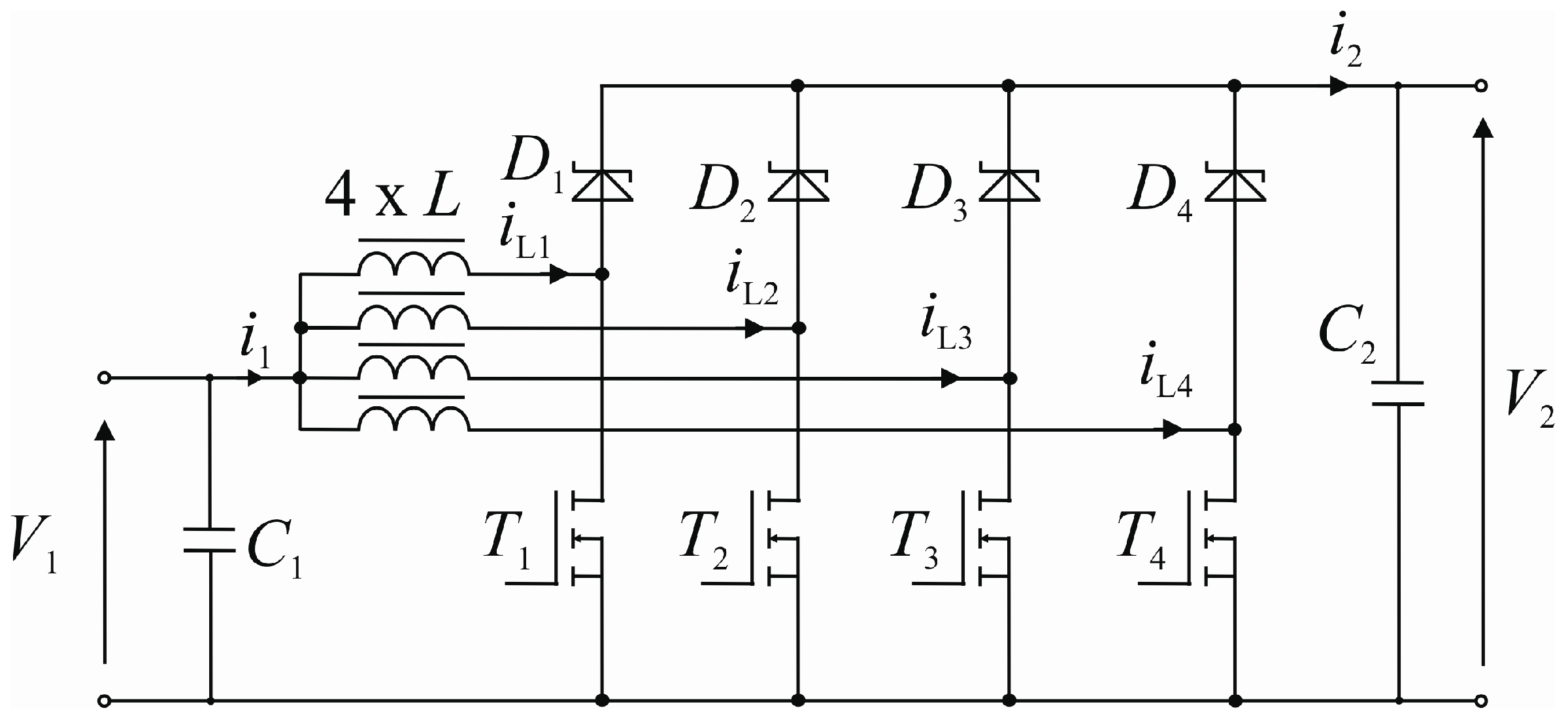
2. Description of the System

This section delivers a set of basic information, relationships and parameters regarding the discussed interleaved DC-DC boost converter (Figure 1). The authors assume that the 6 kW-rated converter is expected to operate as an interface between a DC source (set of the PV panels), where voltage V1 is changing from 290 to 485 V and a DC-input of the Voltage Source Inverter (voltage range V2 = 650–700 V). These values determined operation of the converter with duty cycle from D = 0.25 to D = 0.55.
Then, in the case of the multi-leg topology, ripples of the input current depend on output voltage V2, inductances of inductors L, switching frequency fs = 1/Ts, duty cycle D and, finally, number of legs m. Peak-to-peak value of the ripples in the input current is described by [14]:
i 1 ( p p ) = V 2 ( m O N m D ) d f s L m
where d is the rising coefficient of the current defined as d = tr/τ (tr and τ are the rise time and the period of the input current, respectively), and mON is the number of ON switches during τ.
Taking into account the expected high efficiency and necessary reduction of the size and weight of the inductors, a converter with four legs (m = 4) has been chosen. This number of legs offers a significant cancellation of the current ripples—as can be seen in Figure 2. Calculations which are carried out show superior performance of the four-leg boost converter. In the expected operation range, two points with no ripples can be observed (D = 0.25 and D = 0.5), which refers to 100% reduction in Figure 2b. On the other hand, a single local peak at D = 0.37, which can be observed in Figure 2a, results in reduction by 73% in reference to single-leg boost converter. This means that the inductance of each inductor may be reduced by a factor of 4. An inductance of each of the input inductors has been selected to be equal to 220 µH, taking into account the switching frequency, the duty ratio and the input voltage range. This value is a trade-off between a wide area of the continuous conduction mode operation and small size and weight of the four inductors (4 × 220 µH). On the basis of initial experiences, four separate inductors without coupling were selected as the best trade-offs between low losses and small dimensions, but using coupled inductors will be analyzed in future work. In the first version of the converter, non-optimized inductors were applied. Then, a new set of inductors was designed to improve a system performance. Special attention was paid to an issue of parasitic capacitance, which is recognized as a serious problem. This issue is discussed in the next section.
An increased number of legs and power devices is, on the other hand, accompanied by an increase in the system cost. Therefore, relatively inexpensive SiC power devices have been selected to operate in the designed converter: 1200 V/80 mΩ SiC Metal-Oxide Semiconductor Field-Effect Transistors (MOSFETs) (C2M0080120D) [28] and 1200 V/10 A SiC Schottky diodes (IDH10S120) [29]. Initial calculations prepared on the base of datasheet values suggested that the power losses in semiconductors should not be higher than 1% of the nominal power in the switching frequency range of up to 130 kHz. Obviously, this result is due to an increased chip size of the four 80 mΩ SiC MOSFETs, which seriously reduces the on-state power losses and decreases current stress in these devices.

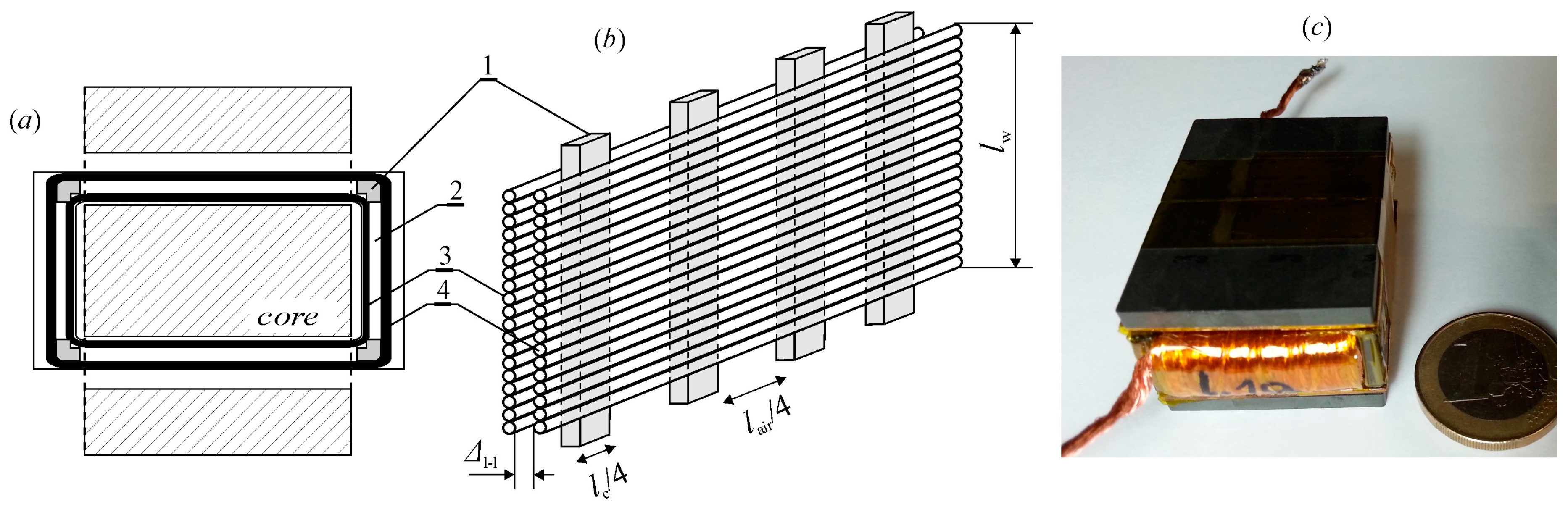
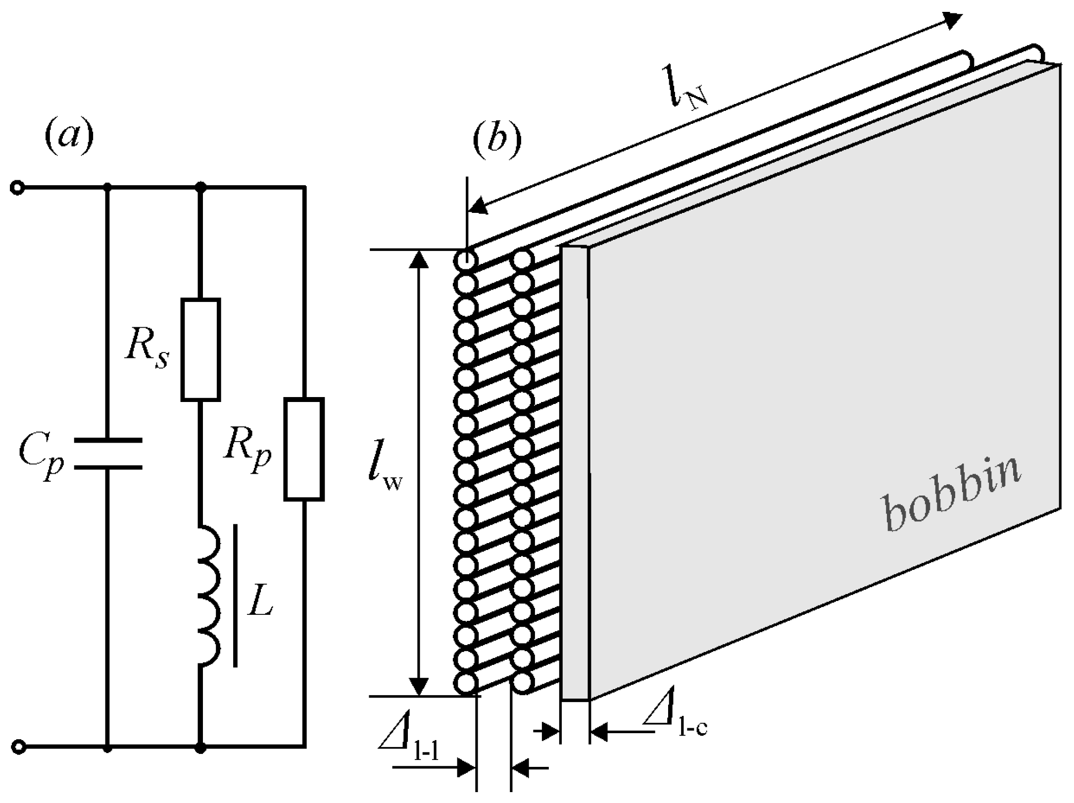
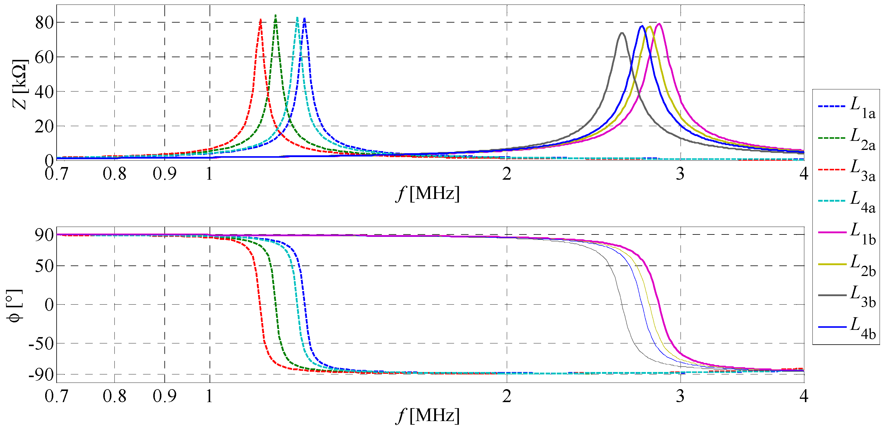
3. Low-Capacitive Inductors

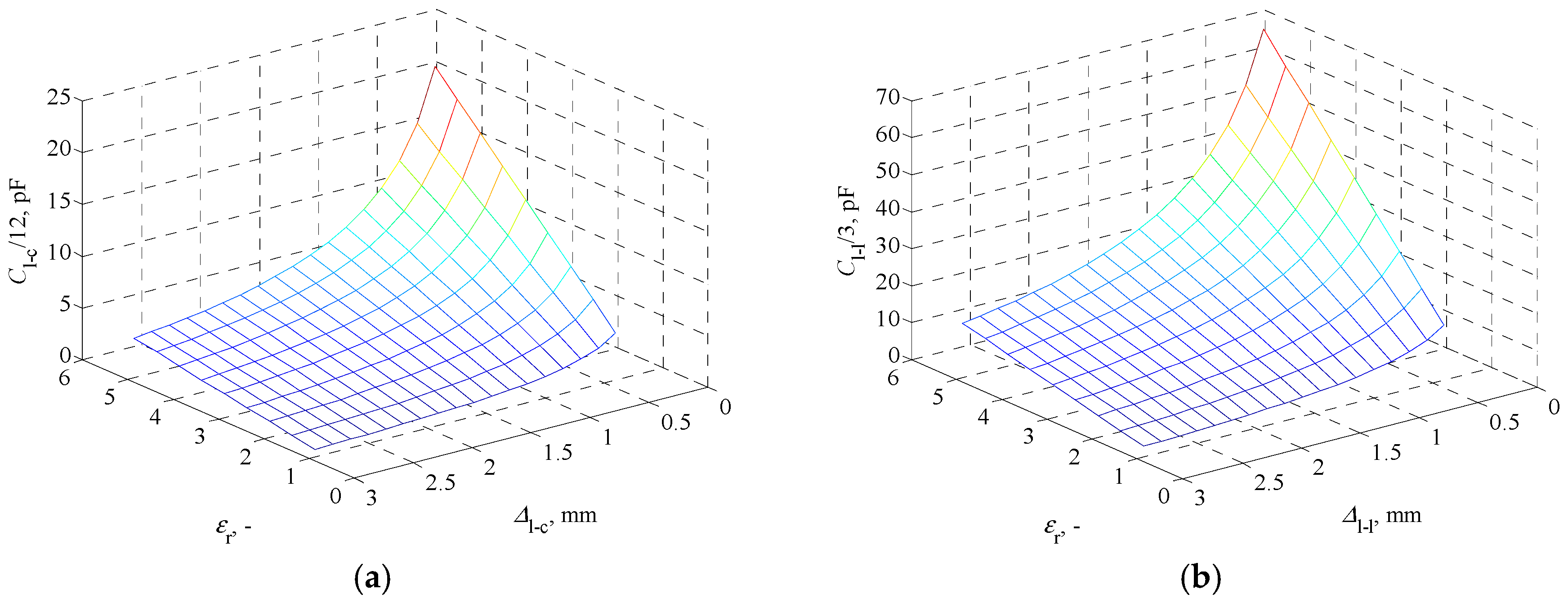
3.1. Parasitic Capacitance of Windings

An equivalent parasitic capacitance (EPC) of an inductor’s windings may be presented as a lumped capacitance Cp marked as the equivalent circuit in Figure 3a. This capacitance is connected in parallel with two branches: resistor Rp, which represents a resistance of the core, and an inductance L in series with resistance of windings Rs. Parasitic capacitance of inductor is basically distributed among wires, layers and the core. It consists of the following capacitances: layer-to-core (Cl-c), turn-to-turn (Ct-t), layer-to-layer (Cl-l) and, in the case of shielded inductors, layer-to-shield (Cl-s) capacitance also appears. The values of Cl-c and Cl-s depend on the distance, permittivity, and, possibly, the grounding of the core and the shield (if applied). A bobbin usually provides a significant distance between the winding and the core, which reduces Cl-c. On the other hand, all components of the Cl-c appear in the parallel leg and the total layer-to-core capacitance may be an important contributor to the EPC. The same can be said about layer-to-layer capacitance Cl-l.
Both capacitances Cl-c and Cl-l can be obtained with the use of the dimensions of the standard inductor winding (Figure 3b):
C l c = ε 0 ε r A l l c
C l l = ε 0 ε r A l l l
where ε0 = 8.85 × 10⁻¹² F/m is the vacuum permittivity; εr is the permittivity of material between layer and core or between layers; A is area of capacitor plate (A = lw lN); ll-c, ll-l are the substitute thickness values of dielectric areas, which can be estimated with the of use simplified equations [30]:
l l c = Δ l c + 1.26 d 0 1.15 ( d 0 2 s ) 2
l l l = Δ l l + 1.26 d 0 1.15 ( d 0 2 s )
where Δl-c, Δl-l are distances between the first layer and the core and between the layers (Figure 3b); d0, s—diameter and insulation thickness of the applied wire, respectively.
The resultant capacitance for double-layer inductor can be estimated according to [31]:
C p = C l c + 4 C l l 12
Based on Equations (2)–(6), the main components (Cl-c and Cl-l) of the resultant winding capacitance (Cp) are plotted in Figure 4 versus permittivity of material εr and versus, respectively, distance between first layer and core Δl-c (Figure 4a) and between layers Δl-l (Figure 4b). As can be seen, reduction of the interlayer capacitance has a significant impact on decrease of the total winding capacitance.

3.2. Low-Capacitive Design

In order to reduce the interlayer capacitance, the authors propose a new method of the winding implementation. The aim is to increase the distance between the layers (Δl-l) and decrease the permittivity value of the dielectric distance between layers, which creates the capacitor between surfaces (see Figure 5a). The authors propose an execution of the windings, which introduces an air gap between layers and provides the smallest possible value of electric permittivity εr (close to unity). The capacitance between layers of winding is formed in a such way that the end of the second layer is at the top of the first one, and a new equation may be introduced:
C l l = 1 l l l ε 0 ( ε a i r A a i r + ε c A c )
where εair—permittivity of the air distance, εc—permittivity of corners distance, and Aair and Ac are surface areas between air distance and corners distances, respectively (see Figure 5b), which can be calculated as follows:
A a i r = l a i r ( a v ) l w
A c = l c ( a v ) l w
where lw is the window length, lair(av) and lc(av) are average values of plates of air and the corners distance, respectively.
Finally, two groups of 220 µH inductors have been designed to operate in the 6 kW DC–DC boost converter. The first group (L1aL4a) was constructed in a classic way, and the second one (L1bL4b) was prepared with the use of 1.5 mm distance between layers (Figure 5c), based on the proposed method. To make a comparison fair, all inductors use the same core type (planar E32/6/20) and material (ferrite 3F3). As the aim is to have four inductors with the same inductance (L = 220 μH) and current rating (IL,p = 9 A), a number of turns were calculated from:
N = L I L , p B p A e
where Bp = 0.25 T is the peak flux density, and Ae = 260 mm2, the effective cross sectional area of the core. The result from (10) is rounded up to N = 30, which is the number of turns of all four inductors. Consideration of high switching frequencies of SiC transistors in a DC-DC converter (up to 130 kHz) skin and proximity effects in the wires must be taken into account. The skin depth δ was calculated from:
δ = 2 ρ c μ ω
where ρc = 23 × 10−9 Ωm is the resistivity of copper at 100 °C, µµ0 is its permeability, and ω is the angular frequency. From Equation (11), the skin depth of a copper wire at 125 kHz is 0.21 mm, and, therefore, a Litz wire with 0.1 mm strands offers a good current distribution in this case.
The parasitic capacitance of all inductors was measured an LCR-8105G impedance analyzer manufactured by GW Instek (New Taipei City, Taiwan). During tests, frequency characteristics were observed (Figure 6) to find the resonance frequencies. Then, parasitic capacitances were calculated using the known value of inductance. According to obtained results, an application of the proposed method offers a reduction of the parasitic capacitance from nearly 80 pF (measured for the classic method, L1aL4a) to 15 pF for optimized inductors (L1bL4b).

4. Laboratory Model of the Four-Leg, 6 kW Interleaved DC-DC Boost Converter
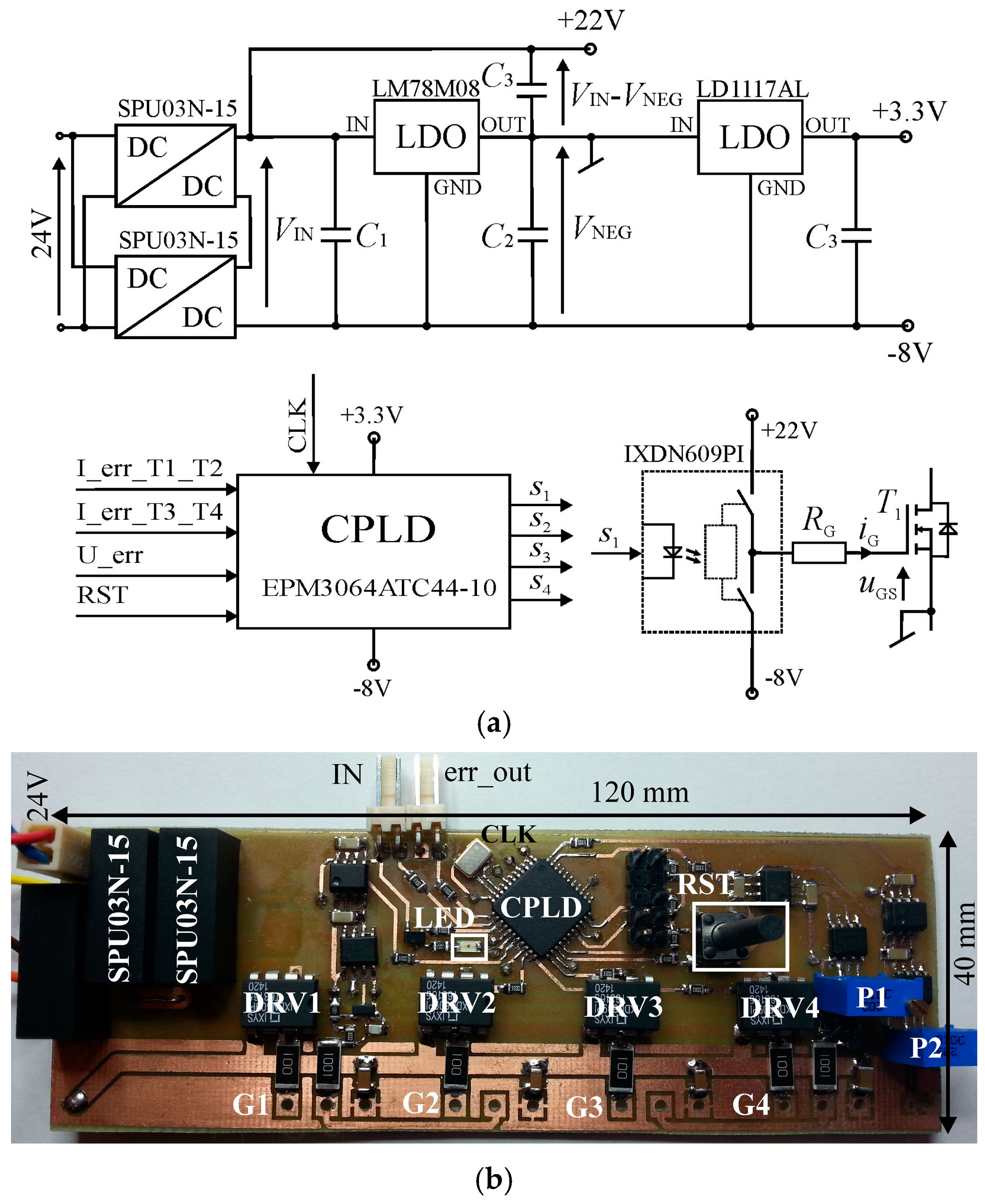
Performance of the magnetic components was verified in the four-leg interleaved boost converter (Figure 1 and Figure 7). It consists of four C2M0080120D SiC MOSFETs (T1–T4) and four IDH10S120 SiC Schottky diodes (D1–D4). Each leg of the converter uses a magnetically independent (without coupling) inductor connected between the positive input pole and middle point of the phase leg. All electrical parameters of semiconductors, inductors and other elements are listed in Table 1.

4.1. System Layout

Power loss estimation leads to the selection of two separate heatsinks (type LAM4-100-SA, Fischer Elektronik, Lüdenscheid, Germany) with dimensions 40 mm × 40 mm × 100 mm. Due to special design of the fins inside, the heatsinks have relatively low thermal resistance value Rth, which is at the level of 0.75 K/W per piece (air-forced cooling with air speed of 24 m3/min provided by an ebm-papst 414 JHH fan). Shape of the heatsink allows for mounting semiconductors or other heat sources on each of the four side walls. With this in mind, a visualization and, then, an experimental model of the DC-DC converter were prepared (Figure 7). All semiconductor elements have been divided into two groups (diodes and transistors) assigned to separate heatsinks to improve electromagnetic interference (EMI) performance.
An additional source of power losses in the system are input inductors (associated with the windings resistances and the equivalent resistance of magnetic cores). Losses of components depend mainly on the current and switching frequency values. In order to avoid an additional cooling system, the inductors were mounted between two heatsinks. Thus, the heat from the inductors is expected to be removed from the converter in the same way as from the semiconductors. The proposed solution is also advantageous for minimizing the length of the connections between middle points of each leg of the converter and the terminals of the magnetic elements. Based on the previously conducted circuit simulation of the converter, the input and output capacitors were also placed in the circuit, respectively (C1 = 220 nF/1000 V and C2 = 6 μF/700 V), and DC decoupling capacitors (4 × 47 nF/1000 V) were connected near the semiconductor terminals. Finally, the size of the converter is 125 mm × 100 mm × 60 mm (Figure 7b), which results in a volume value of the main circuit below 1 dm3 (power density 8 kW/dm3).

4.2. Gate Driver and Protection
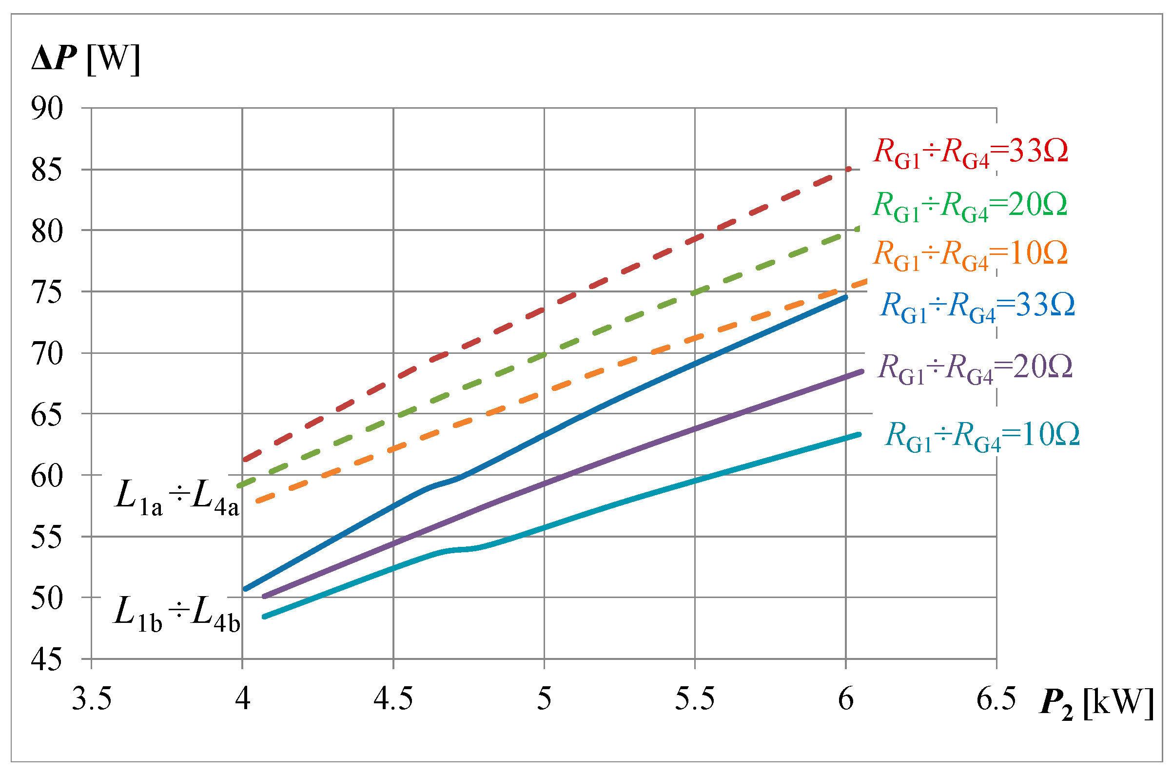
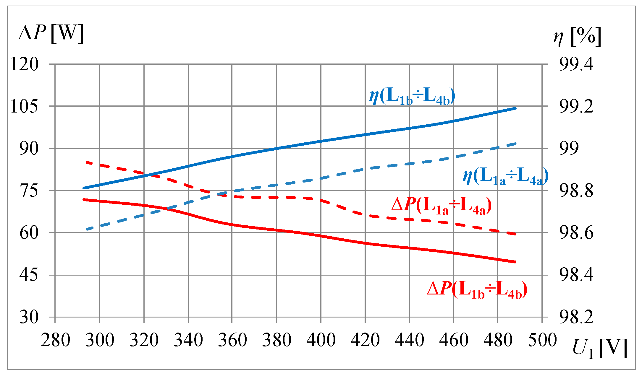
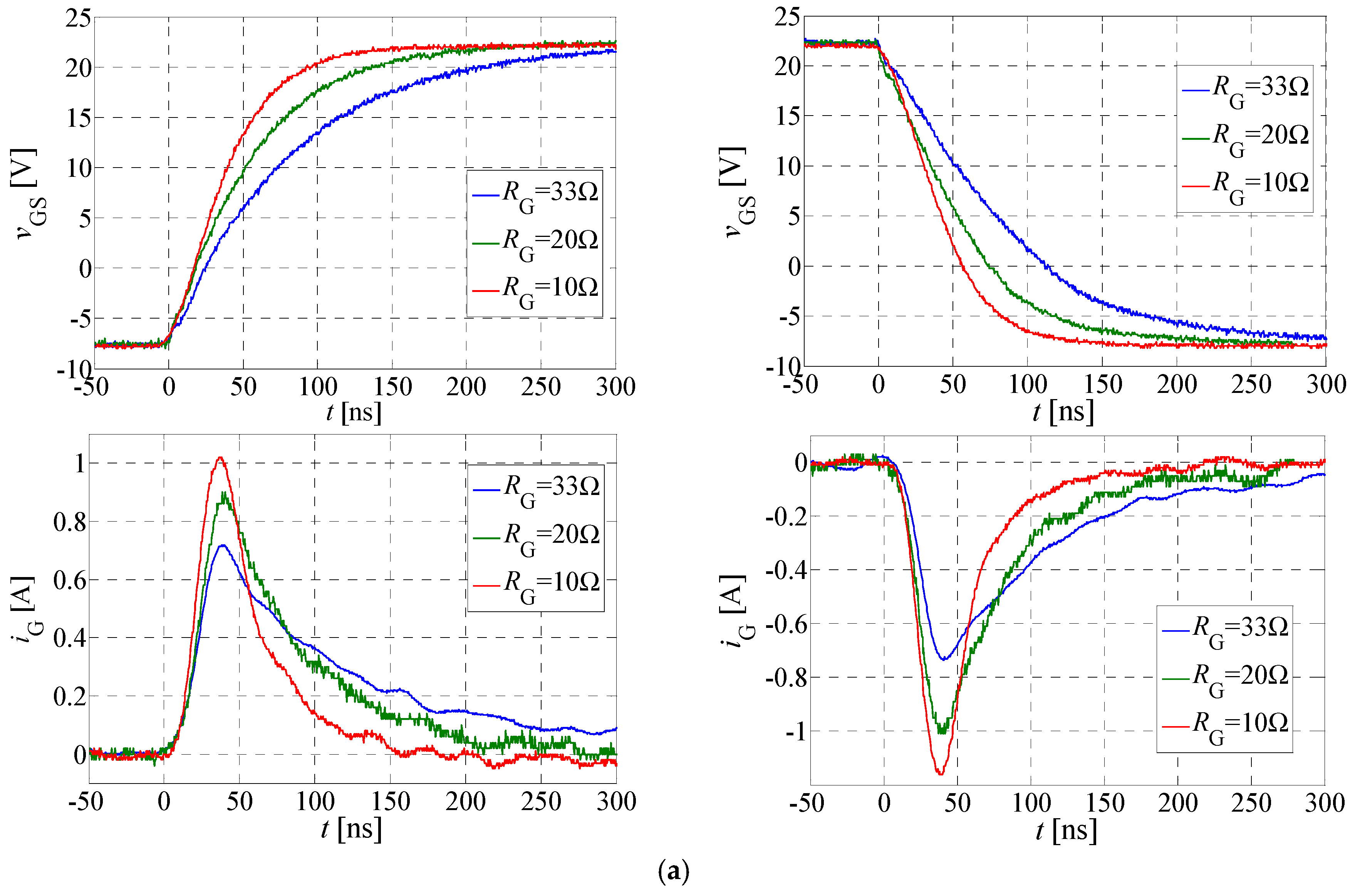
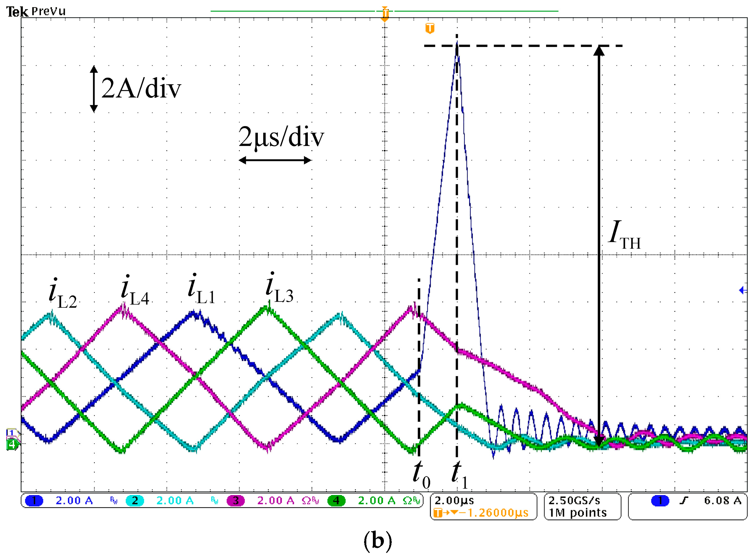
A special design of the gate drivers with protection circuits was developed in order to control and protect semiconductor devices used in the considered converter (Figure 8a). The same control pulse with an identical duty ratio should be provided to all four SiC MOSFETs with suitable phase shift and, therefore, dedicated logic circuits are applied. The gate driver, which is presented in Figure 8, consists of a Complex Programmable Logic Device (CPLD) EPM3064ATC44-10N from MAX 3000A series made by ALTERA (San Jose, CA, USA) as a main control unit with a 100 MHz oscillator as a global clock (CLK) (Figure 8b). To generate four output signals (s1s4) at frequencies of up to 130 kHz, 10-bit up counter was used. Additionally, a reset (RST) signal was also implemented as an input signal of ALTERA to manually reset the errors when, for example, short circuit or overvoltage protection system would be activated. The CPLD output signals are connected to the gate driver units controlling four SiC MOSFETs.
According to manufacturer recommendations, the positive supply voltage of the gate drivers is set to 22 V, while negative bias equals −8 V. In order to ensure asymmetric division of the 30 V supply voltage, a special circuit with a Low-Dropout (LDO) regulator was designed. Outputs of the DC-DC converters (two SPU03N-15 (MEAN WELL, New Taipei City, Taiwan) from Mean Well connected in series) are connected to the voltage regulator (LM78M08) (STMicroelectronics, Switzerland, Geneva), which provides VNEG = 8 V in reference to the negative pole of the converter. Due to the use of capacitors C2 and C3 (4.7 μF/50 V), it is possible to obtain the voltage of the upper capacitor (C3), which is a difference between the output voltage of the DC-DC converter (VIN) and the regulated voltage at C2. This voltage is close to 22 V and is applied as a positive supply voltage for a fast totem-pole driver IXDN609PI (IXYS Corporation, Milpitas, CA, USA).
The gate driver was tested before the application in the DC-DC converter. Firstly, the gate-source voltage vGS and gate current iG were observed for different values of gate resistance RG. Obtained records (see Figure 9a) show a proper operation of the gate driver and indicate an impact of the gate resistance value on dynamic properties of the driving process (dvGS/dt and diG/dt). Protection circuits (over-current and over-voltage), included in the gate driver, were also tested. Selected results from those tests have been presented in Figure 9b. During the steady-state operation of the converter, inductor from one of the legs (L1) was shorted (time t0), which led to an increase of the current iL1 value and, finally, to an activation of the protection system (an assumed threshold current was equal to ITH at time t1). Presented waveforms are a little unbalanced, which may be related to the short-circuit state and an additional switch, which was necessary to trigger the short-circuit condition. The lack of balance is not visible under steady-state operation of converter.

5. Experiments

The experimental model discussed above was connected to the DC supply and loaded with a resistor. Transistors were operating with a phase shift of 90° and a switching frequency fs = 125 kHz, while the rated power of the converter was Pn = 6 kW at the input voltage V1 changing in the range of from 290 to 485 V. In the first test, the converter contained two standard inductors (L1a, L2a) and two low-capacitive inductors (L1b, L2b) built with the described method. Oscilloscope records have been saved in order to verify the presented considerations regarding the impact of the parasitic capacitance of the magnetic components on the quality of the current waveforms in the DC-DC converter. Waveforms of the inductor currents presented in Figure 10 show that iL1a and iL2a are characterized by high-frequency oscillations (in the range of 1 MHz) during each switching process. This effect is almost invisible in two legs containing the inductors with low parasitic capacitance (L1b, L2b), where initial spikes are very small and the oscillations decay very quickly. Thus, a decrease of EPC and an increase in the SRF (Self-Resonant Frequency) of the applied inductors have a huge impact on the performance of the boost converter.
In the next step, an impact of the parasitic capacitance of the inductors was tested by means of power loss measurement. The precision power analyzer Yokogawa 1800 (Tokyo, Japan) was applied to determine power losses (ΔP) and efficiency (η) of the tested converter. At first, the system was tested with four inductors made in a classic way—L1aL4a and with three values of the gate resistors (RG1RG4 = 33 Ω, 20 Ω and 10 Ω). The power was varied from 4 to 6 kW (V2 = 650 V). Then, low-capacitive inductors (L1bL4b) were applied and the same test was repeated—see Figure 11. It is clearly visible that the system with new, low-capacitive inductors shows lower power loss values, from 10.4 to 12.5 W at 6 kW. Obviously, lower gate resistance increases switching speed in both cases, but an impact of the RG reduction from 33 Ω to 10 Ω is more evident for low-capacitive inductors as high-frequency resonances are limited. Examples of screens obtained during power loss measurements for different inductors have been presented in Figure 12.
Another set of power loss measurements was performed according to changes in the input voltage V1, while the duty cycle range has been adjusted. Figure 13 contains the results obtained at the nominal power Pn = 6 kW and with assumed input voltage range V1 = 290–485 V (D = 0.25–0.55). The experiment was conducted with gate resistor values RG = 10 Ω and using two types of inductors again. The obtained results show that the efficiency is rising with the input voltage (lower input current) and for the standard inductors L1aL4a, is in the range from 98.6% to 99% (which corresponds to total power loss values between 84.8 W and 59.6 W). Low capacitive inductors L1bL4b increase efficiency to the range 98.8%–99.2%, which corresponds to the power loss values between 71.9 W and 49.4 W. The difference in the power loss values is 12.9 W for V1 = 290 V (D = 0.55) and 10.2 W for V1 = 485 V (D = 0.25).
In order to achieve electro-thermal steady state, the DC-DC converter was also tested under nominal conditions for 130 min (Figure 14). The results of the tests show that the converter is also characterized by high thermal stability. After approximately 30 min, the power losses remained constant. The reason is that, on the one hand, thermal capacitances are rather low (small dimensions of the SiC chips, inductors and heatsinks), and, on the other hand, the power losses in SiC devices have low temperature dependence.
Finally, selected results for fs = 125 kHz, Pn = 6 kW, V2 = 650 V and D = 0.45 have been compared with analytical calculations and presented in Figure 15. The calculations of power losses in semiconductor devices were based on the datasheet values and assumed electrical parameters (frequency, transistor and diode currents and voltages). Estimation of core losses (P_Fe) in the inductors have been prepared with the use of well-known Steinmetz equations (iGSE—improved Generalized Steinmetz Equation) for ferrite type material 3F3 [32,33]. The winding power losses (P_Cu) were calculated on the basis of effective value of the inductor current and winding resistance obtained for individual harmonics determined for non-sinusoidal winding current [34].

6. Conclusions

The highly-efficient and compact interleaved boost converter with SiC power devices rated at 6 kW is presented and investigated in this paper. In particular, two types of the input inductors with the same number of turns and the same type of cores in co-operation with fast switching semiconductor devices were compared. The converter with conventionally wound, non-optimized inductors suffered from oscillations of the current during each switching process. In the same conditions, low-capacitive inductors showed very limited amplitude of oscillations during switching processes and the power losses of the converters dropped by up to 25%. Aside from high efficiency recorded (above 99%), the developed system shows high power density of about 8 kW/dm3. It proves that the presented combination of wide bandgap semiconductors, the interleaving technique and the optimized parasitic capacitance of inductors bring noticeable performance improvement to the DC-DC boost converters.

Acknowledgments

This work was partially supported by the statutory fund of the Faculty of Electrical Engineering, the Warsaw University of Technology and by the project "The comprehensive power electronics system with Silicon Carbide (SiC) devices as applicable to renewable energy sources and improving their quality" which was realized within the Ventures programme of Foundation for Polish Science, co-financed by European Union, Regional Development Fund.

Author Contributions

Mariusz Zdanowski designed the prototype, performed the experiments and wrote this paper with Jacek Rabkowski and Roman Barlik who analyzed the data and help to prepare structure of paper. All authors read and approved the manuscript.

Conflicts of Interest

The authors declare no conflict of interest.

References

  1. Milan, J.; Gondignon, P.; Perpina, X.; Perez-Tomas, A.; Rebollo, J. A survey of wide bandgap power semiconductor devices. IEEE Trans. Power Electron. 2014, 29, 2155–2163. [Google Scholar] [CrossRef]
  2. Rabkowski, J.; Peftitsis, D.; Nee, H.P. SiC power transistors—A new era in power electronics is initiated. IEEE Ind. Electron. Mag. 2012, 6, 17–26. [Google Scholar] [CrossRef]
  3. Biela, J.; Schweizer, M.; Waffler, S.; Kolar, J.W. SiC vs. Si—Evaluation of potentials for performance improvement of inverter and DC-DC converter systems by SiC power semiconductors. IEEE Trans. Ind. Electron. 2011, 58, 2872–2882. [Google Scholar] [CrossRef]
  4. Zhao, C.; Trento, B.; Jiang, L.; Jones, E.A.; Liu, B.; Zhang, Z.; Costinett, D.; Wang, F.F.; Tolbert, L.M.; Jansen, J.F.; et al. Design and implementation of a GaN-based, 100 kHz, 102-W/In3 single-phase inverter. IEEE J. Emerg. Sel. Top. Power Electron. 2016, 4, 824–840. [Google Scholar] [CrossRef]
  5. Zhong, X.; Wu, X.; Zhou, W.; Cheng, S.; Cheng, K. Design and experimental analysis of a 1 kW, 800 kHz, all-SiC boost DC-DC converter. In Proceedings of the Twenty-Ninth Annual IEEE Applied Power Electronics Conference and Exposition (APEC), Fort Worth, TX, USA, 16–20 March 2014; pp. 488–492.
  6. Whitaker, B.; Barkley, A.; Cole, Z.; Passmore, B.; Martin, D.; McNutt, T.R.; Lostetter, A.B.; Lee, J.S.; Shiozaki, K. A high-density, high-efficiency, isolated on-board vehicle battery charger utilizing silicon carbide power devices. IEEE Trans. Power Electron. 2013, 29, 2606–2617. [Google Scholar] [CrossRef]
  7. Rabkowski, J.; Peftitsis, D.; Nee, H.-P. Design steps toward a 40-kVA SiC JFET inverter with natural-convection and an efficiency exceeding 99.5%. IEEE Trans. Ind. Appl. 2013, 49, 1589–1598. [Google Scholar] [CrossRef]
  8. Abou-Alfotouh, A.M.; Radun, A.V.; Chang, H.-R.; Winterhalter, C. A 1-MHz hard-switched silicon carbide DC-DC converter. IEEE Trans. Power Electron. 2006, 21, 880–889. [Google Scholar] [CrossRef]
  9. Bosshard, R.; Kolar Johann, W. All-SiC 9.5 kW/dm3 on-board power electronics for 50 kW/85 kHz automotive IPT system. IEEE J. Emerg. Sel. Top. Power Electron. 2016, 5, 419–431. [Google Scholar] [CrossRef]
  10. Hu, Y.; Cao, W.; Finney, S.J.; Xiao, W.; Zhang, F.; McLoone, S.F. New modular structure DC-DC converter without electrolytic capacitors for renewable energy applications. IEEE Trans. Sustain. Energy 2014, 5, 1184–1192. [Google Scholar] [CrossRef]
  11. Hu, Y.; Zeng, R.; Zhang, J.; Finney, S.J. Design of a modular, high step-up ratio DC-DC converter for HVDC applications integrating offshore wind power. IEEE Trans. Ind. Electron. 2016, 63, 2190–2202. [Google Scholar] [CrossRef]
  12. Agamy, M.S.; Chi, S.; Elasser, A.; Harfman-Todorovic, M.; Jiang, Y.; Mueller, F.; Tao, F. A high-power-density DC-DC converter for distributed PV architectures. IEEE J. Photovolt. 2013, 3, 791–798. [Google Scholar] [CrossRef]
  13. Huang, X.; Lee Fred, C.; Li, Q.; Du, W. High-frequency high-efficiency GaN-based interleaved CRM bidirectional buck/boost converter with inverse coupled inductor. IEEE Trans. Power Electron. 2016, 31, 4343–4352. [Google Scholar] [CrossRef]
  14. Choe, G.-Y.; Kim, J.-S.; Kang, H.-S.; Lee, B.-K. An optimal design methodology of an interleaved boost converter for fuel cell applications. J. Electr. Eng. Technol. 2010, 5, 319–328. [Google Scholar] [CrossRef]
  15. Hegazy, O.; Mierlo, J.V.; Lataire, P. Analysis, modeling, and implementation of a multidevice DC/DC converter for fuel cell hybrid electric vehicles. IEEE Trans. Power Electron. 2012, 27, 4445–4458. [Google Scholar] [CrossRef]
  16. Zhang, X.; Mattavelli, P.; Boroyevich, D. Impact of interleaving on input passive components of paralleled DC–DC converters for high power PV applications. In Proceedings of the 15th International Power Electronics and Motion Control Conference (EPE-PEMC), Novi Sad, Serbia, 4–6 September 2012; pp. LS7d.5-1–LS7d.5-6.
  17. Kosai, H.; Scofield, J.; McNeal, S.; Jordan, B.; Ray, B. Design and performance evaluation of a 200 °C interleaved boost converter. IEEE Trans. Power Electron. 2013, 28, 1691–1699. [Google Scholar] [CrossRef]
  18. Liu, J.; Wong, K.L.; Allen, S.; Mookken, J. Performance evaluations of hard-switching interleaved DC/DC boost converter with new generation silicon carbide MOSFETs. In Proceedings of the Annual Conference of the IEEE Industrial Electronics Society (IECON), Vienna, Austria, 10–13 November 2013; pp. 1157–1162.
  19. Gu, Y.; Zhang, D. Interleaved boost converter with ripple cancellation network. IEEE Trans. Power Electron. 2013, 28, 3860–3869. [Google Scholar] [CrossRef]
  20. Magne, P.; Liu, P.; Bilgin, B.; Emadi, A. Investigation of impact of number of phases in interleaved DC-DC boost converter. In Proceedings of the IEEE Transportation Electrification Conference and Expo (ITEC), Metro Detroit, MI, USA, 14–17 June 2015; pp. 1–6.
  21. Martinez, W.; Kimura, S.; Imaoka, J.; Yamamoto, M.; Cortes, C.A. Volume comparison of DC-DC converters for electric vehicles. In Proceedings of the IEEE Workshop on Power Electronics and Power Quality Applications (PEPQA), Bogota, Colombia, 2–4 June 2015; pp. 1–6.
  22. Mouli, G.R.C.; Schijffelen, J.; Bauer, P.; Zeman, M. Design and comparison of a 10kW interleaved boost converter for PV application using Si and SiC devices. IEEE J. Emerg. Sel. Top. Power Electron. 2016, PP. [Google Scholar] [CrossRef]
  23. Velandia, F.; Martinez, W.; Cortes, C.A.; Noah, M.; Yamamoto, M. Power loss analysis of multi-phase and modular interleaved boost DC-DC converters with coupled inductor for electric vehicles. In Proceedings of the 18th European Conference on Power Electronics and Applications (EPE’16 ECCE Europe), Karlsruhe, Germany, 5–9 September 2016; pp. 1–10.
  24. Jang, J.; Pidaparthy, S.K.; Lee, S.; Choi, B. Performance of an interleaved boundary conduction mode boost PFC converter with wide band-gap switching devices. In Proceedings of the IEEE 2nd International Future Energy Electronics Conference (IFEEC), Taipei, Taiwan, 1–4 November 2015.
  25. Zdanowski, M.; Rabkowski, J.; Barlik, R. Design issues of the high-frequency interleaved DC/DC boost converter with silicon carbide MOSFETs. In Proceedings of the 16th European Conference on Power Electronics and Applications (EPE’14-ECCE Europe), Lappeenranta, Finland, 26–28 August 2014; pp. 1–10.
  26. Zdanowski, M.; Kostov, K.; Rabkowski, J.; Nee, H.P. The role of the parasitic capacitance in boost converters with normally-on SiC JFETs. In Proceedings of the 7th International Power Electronics and Motion Control Conference (IPEMC), Harbin, China, 2–5 June 2012; pp. 1842–1847.
  27. Zdanowski, M.; Kostov, K.; Rabkowski, J.; Barlik, R.; Nee, H.P. Design and evaluation of reduced self-capacitance inductor in DC/DC converters with fast-switching SiC transistors. IEEE Trans. Power Electron. 2014, 29, 2492–2499. [Google Scholar] [CrossRef]
  28. C2M0080120D Datasheet from Cree Inc. Available online: www.cree.com (accessed on 10 February 2017).
  29. IDH10S120 Datasheet from Infineon Technologies AG. Available online: www.infineon.com (accessed on 10 February 2017).
  30. Snelling, E.C. Soft Ferrities—Properties and Applications; Chemical Rubber Company (CRC): Boca Raton, FL, USA, 1969. [Google Scholar]
  31. Weber, S.; Schinkel, M.; Guttowski, S.; John, W.; Reichl, H. Calculating parasitics capacitance of three-phase common-mode chokes. In Proceedings of the Power Conversion Intelligent Motion (PCIM), Nuremberg, Germany, 20–25 May 2005; pp. 1–6.
  32. Venkatachalani, K.; Sullivan, C.R.; Abdallah, T.; Tacca, H. Accurate prediction of ferrite core loss with nonsinusoidal waveforms using only Steinmetz parameters. In Proceedings of the IEEE Workshop on Computers in Power Electronics, Mayaguez, Puerto Rico, 3–4 June 2002; pp. 36–41.
  33. Hurley, W.G.; Wölfle, W.H. Transformers and Inductors for Power Electronics: Theory, Design and Applications; John Wiley & Sons: Hoboken, NJ, USA, 2013. [Google Scholar]
  34. Kondrath, N.; Kazimierczuk, M.K. Inductor winding loss owing to skin and proximity effects including harmonics in non-isolated pulse-width modulated DC-DC converters operating in continuous conduction mode. IET Power Electron. 2010, 3, 989–1000. [Google Scholar] [CrossRef]
Figure 1. Scheme of the four-leg interleaved boost converter.
Energies 10 00363 g001
Figure 2. (a) Percentage of the input current ripples for the single-, two- and four-leg(s) configuration of converter and (b) percentage reduction of current ripples due to interleaving of converter legs relative to one-leg converter.
Energies 10 00363 g002
Figure 3. (a) Equivalent circuit with lumped parameters of winding and (b) graphical presentation of two-layers standard wound inductor.
Energies 10 00363 g003
Figure 4. (a) Dependence of material permittivity (εr) and distance between core and first layer Δl-c and (b) two layers Δl-l on parasitic capacitance of designed inductors.
Energies 10 00363 g004
Figure 5. (a,b) Graphical representation of two-layer inductor constructed using the proposed method, where: 1—corners, 2—air distance between layers, 3 and 4—first and second layer and (c) inductor’s picture compared with 1 euro coin.
Energies 10 00363 g005
Figure 6. Impedance characteristics of two sets of four inductors.
Energies 10 00363 g006
Figure 7. (a) A visualization and (b) a picture of the four-leg interleaved boost converter prototype.
Energies 10 00363 g007
Figure 8. The gate driver for the interleaved DC-DC converter: (a) scheme and (b) photo of the prototype.
Energies 10 00363 g008
Figure 9. The gate driver for the interleaved DC-DC converter: measured waveforms of the gate-source voltages vGS and gate currents iG in case of different gate resistance values: (a) 33 Ω (blue), 20 Ω (green) and 10 Ω (red) and (b) waveforms of inductors current iL1 during the short-circuit state.
Energies 10 00363 g009aEnergies 10 00363 g009b
Figure 10. Waveforms of the inductor currents in the DC-DC converter operating with inductors made in a classic way (L1a, L2a) and with inductors made with the proposed method (L1b, L2b).
Energies 10 00363 g010
Figure 11. Power losses (ΔP) of the converter obtained at various output power P2 values and gate resistance values (RG1RG4 = 33 Ω; = 20 Ω; = 10 Ω) and different types of input inductors (L1aL4a; L1bL4b); fs = 125 kHz, D = 0.45.
Energies 10 00363 g011
Figure 12. Power losses (ΔP) of the converter obtained at different output power P2 and gate resistance values (RG1RG4 = 33 Ω; = 20 Ω; = 10 Ω) and type of input inductors (L1aL4a; L1bL4b); fs = 125 kHz, D = 0.45.
Energies 10 00363 g012
Figure 13. Power losses (ΔP) and efficiency (η) versus input voltage (duty cycle) obtained at fs = 125 kHz, Pn = 6 kW, with use of different types of input inductors: L1aL4a (dotted lines) or L1bL4b (solid lines).
Energies 10 00363 g013
Figure 14. Power losses (ΔP) and efficiency (η) versus time of steady-state operating, obtained at fs = 125 kHz, Pn = 6 kW, D = 0.45 with use of different types of input inductors: L1aL4a (dotted lines) or L1bL4b (solid lines).
Energies 10 00363 g014
Figure 15. Comparison of power losses (ΔP) at different types of input inductors: L1aL4a or L1bL4b and gate resistors (RG1RG4 = 33 Ω; = 20 Ω; = 10 Ω).
Energies 10 00363 g015
Table 1. Converter parameters.
SymbolQuantityValue
V1input voltage range290–485 V
V2output voltage range650–700 V
Pnnominal power6 kW
Dduty cycle range0.25–0.55
fsswitching frequency4 × 125 kHz
L1L4inductance of input inductors220 μH
IL_minductor maximum current9 A
C1input capacitor220 nF/1 kV
C2output capacitor6 μF/700 V + 4 × 47 nF/1 kV
T1T4SiC transistors1.2 kV/80 mΩ (C2M0080120D)
D1D4SiC diodes1.2 kV/10 A (IDH10S120)

