Article

A Novel High Step-Up DC-DC Converter with Coupled Inductor and Switched Clamp Capacitor Techniques for Photovoltaic Systems

1
Department of Electrical Engineering, National Cheng Kung University, No. 1 University Road, Tainan 701, Taiwan
2
Power Supply Group, National Synchrotron Radiation Research Center, 101, Hsin-Ann Road, Hsinchu 300, Taiwan
3
Mission Critical Infrastructure Solutions Business Unit, Delta Electronics INC, 39 Section 2, Huan-dong Road, Shanhua Township, Tainan 741, Taiwan
*
Author to whom correspondence should be addressed.
Energies 2017, 10(3), 378; https://doi.org/10.3390/en10030378
Submission received: 9 September 2016 / Revised: 7 March 2017 / Accepted: 10 March 2017 / Published: 16 March 2017

Abstract

:
In this study, a novel high step-up DC-DC converter was successfully integrated using coupled inductor and switched capacitor techniques. High step-up DC-DC gain was achieved using a coupled inductor when capacitors charged and discharged energy, respectively. In addition, energy was recovered from the leakage inductance of the coupled inductor by using a passive clamp circuit. Therefore, the voltage stress of the main power switch was almost reduced to 1/7 Vo (output voltage). Moreover, the coupled inductor alleviated the reverse-recovery problem of the diode. The proposed circuit efficiency can be further improved and high voltage gain can be achieved. The operation principle and steady-state analysis of the proposed converter were discussed. Finally, a hardware prototype circuit with input voltage of 24 V, output voltage of up to 400 V, and maximum power of 150 W was constructed in a laboratory; the maximum efficiency was almost 96.2%.

1. Introduction

In recent years, air pollution and energy shortage have become major national concerns. When the global temperature increases by 1 °C, the sea level will increase by 2.3 m [1]. This phenomenon will considerably affect human life and safety. Therefore, previous studies have attempted to find a solution, hoping to solve the problems of air pollution, global warming, and energy shortage by using highly efficient renewable energy systems. The current more mature and widely used renewable energy sources include solar, wind, and tidal energy sources [2,3,4]. Often these renewable energy sources have low-voltage output and must pass through a set of high boost converter circuits to increase the voltage, and then through a DC-AC inverter to convert AC voltage from the main supply in parallel. Therefore, a DC-DC high boost ratio circuit affects the overall efficiency of the system [5,6,7,8].
The conventional DC-DC boost circuit is not applied in high boost ratio applications. In an ideal scenario, when the duty cycle in a conventional boost circuit increases to 1 (unity), the boost conversion ratio reaches infinity. However, high step-up gain is limited by the capacitor, inductor main power switch, and resistance, because electromagnetic interference and reverse-recovery issues are encountered at extreme duty cycles. Moreover, the leakage inductance of the transformer will cause high power dissipation and high voltage spikes on the main power switch. Therefore, a main power switch with high stress voltage must be selected because of excessive cost and space issues. Therefore, many studies have developed a new architecture to overcome the shortcomings of a conventional boost circuit. In particular, switch capacitor [9,10,11,12,13], coupled inductor [14,15,16,17,18,19,20,21], and voltage lift [22,23] techniques have been proposed. A coupled inductor step-up circuit with a simple inductive winding structure was used to achieve low voltage stress of the main switch and a high voltage conversion ratio. Therefore, this architecture is commonly used. However, the main drawback of this architecture is that the coupled inductor has a considerable leakage inductance; this leakage inductance and parasitic capacitance on the switch will resonate and cause voltage spikes. To solve the problems caused by leakage inductance, capacitors, resistors, and diodes comprising a snubber circuit can be used; however, the energy is consumed in the resistance, thus reducing circuit efficiency. Switched capacitor and voltage lift technology can achieve a high boost ratio function but the main switch suffers a high transient current, and the conduction loss is increased. A switched-clamp capacitor can store energy when the switch is turned on. When the power is switched off afterwards, the energy in the capacitor is delivered to the output loading. However, the electric system prevents current flow and no direct conduction path is permitted. The voltage lift technique is similar the Cuk converter or the single-ended primary inductor converter (SEPIC) converter, the energy transfer from one inductor via the intermediate capacitor and then to the other inductor. Therefore, the transferred energy is mainly determined by the capacitance, thus causing the current stress on the capacitor to be serious. The coupled-inductor technique can achieve high step-up gain by adjusting the turn ratio. However, the inductor leakage issue relates to the voltage spike on the power switch. Therefore, this study used a coupled inductor step-up circuit with a clamp circuit, which absorbed energy from the leakage inductor of the coupled inductor and supply the energy back to the output terminal of the capacitor during the next period [24,25]. Using a clamp circuit prevents spikes on the switch, and the main switch voltage stress is clamped at a voltage of 1/7 Vo. Moreover, the booster-circuit integrates a boost-flyback converter with switched capacitor architecture to achieve a high step-up ratio. This circuit has boost and flyback type features. When the switch is turned on, the first boost stage is similar to a boost converter combined with a switched capacitor converter. Conversely, when the switch is turned off, the second boost stage is similar to the flyback and switched capacitor converters [26,27,28,29,30,31,32,33,34]. The new proposed converter architecture can achieve a high step-up ratio by adjusting the duty cycle; a clamp circuit is used for energy recovery by the leakage inductor of the coupled inductor to achieve high efficiency and step-up ratio.

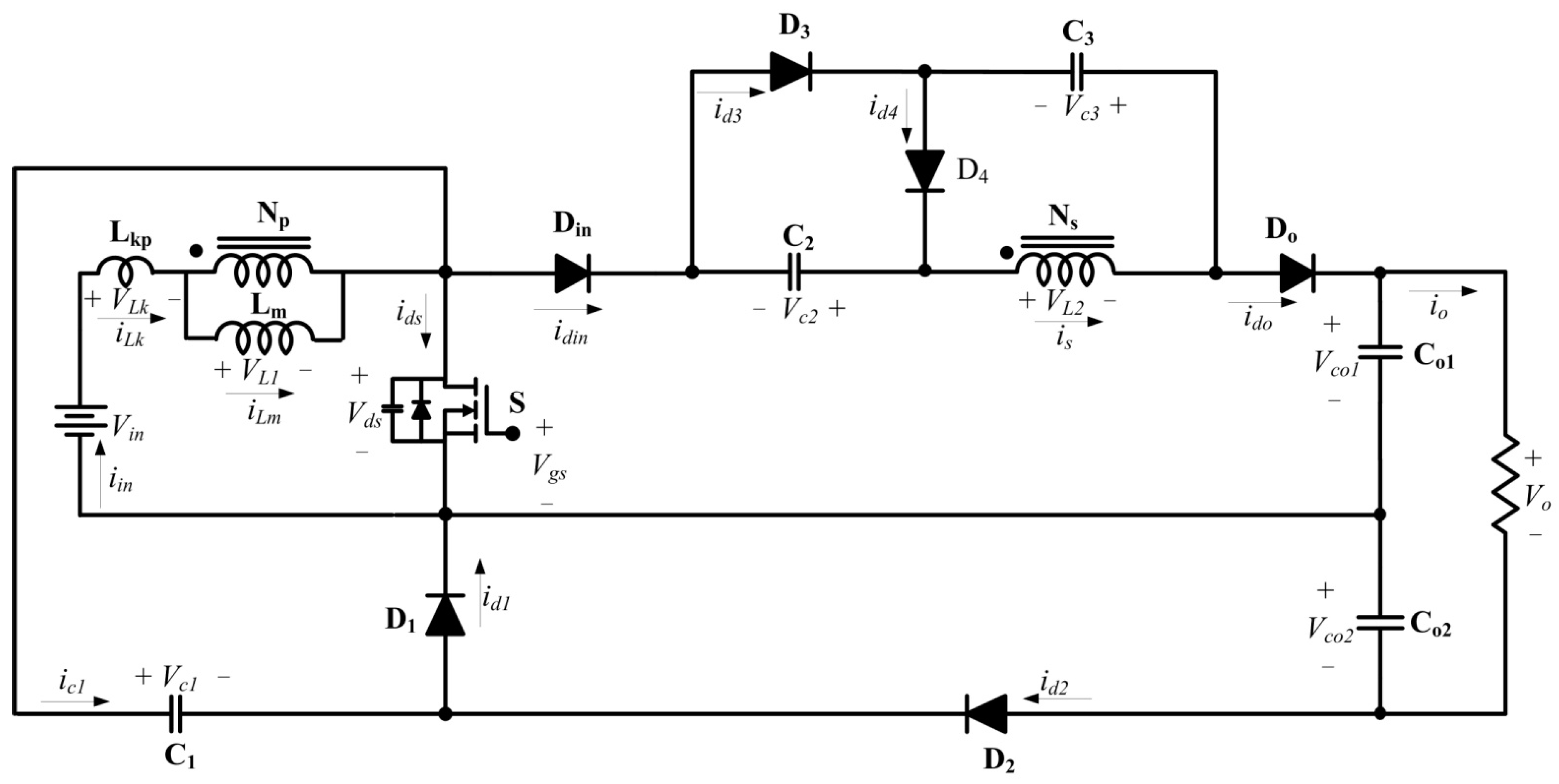
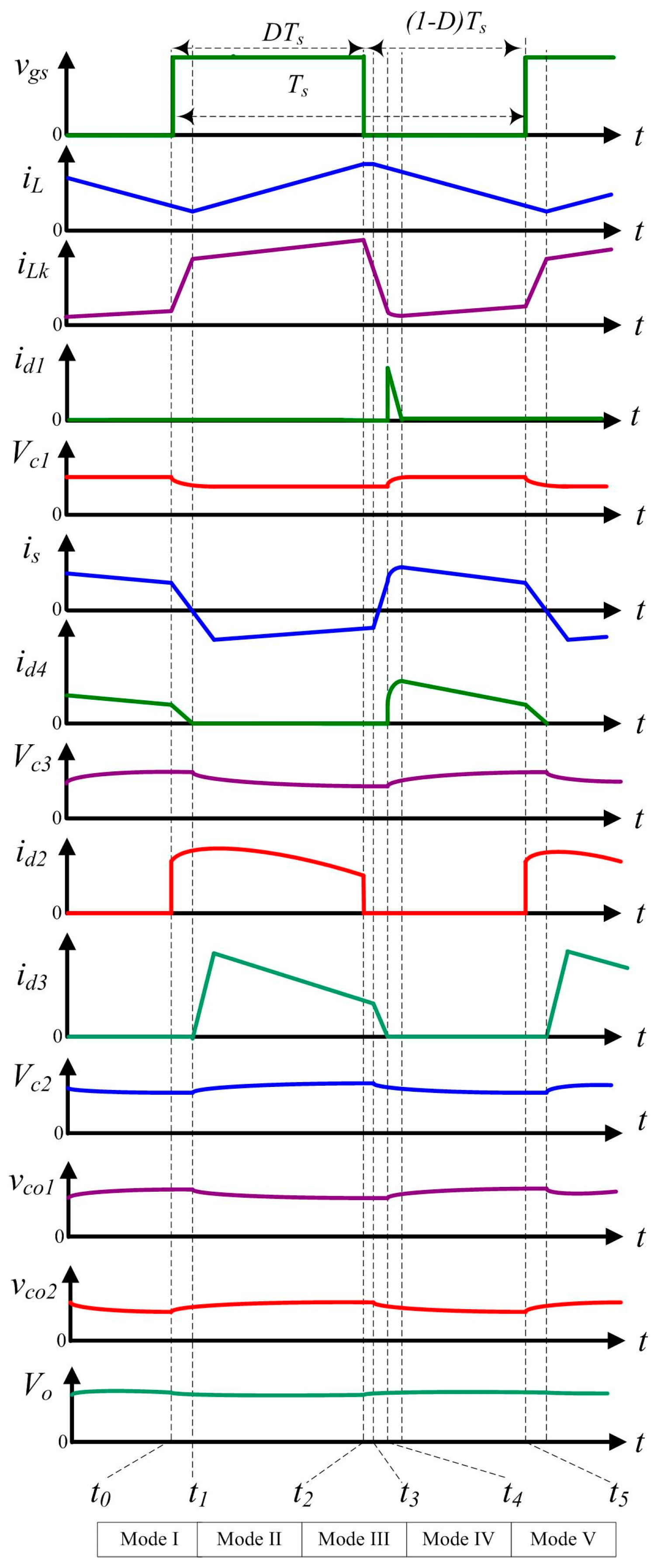
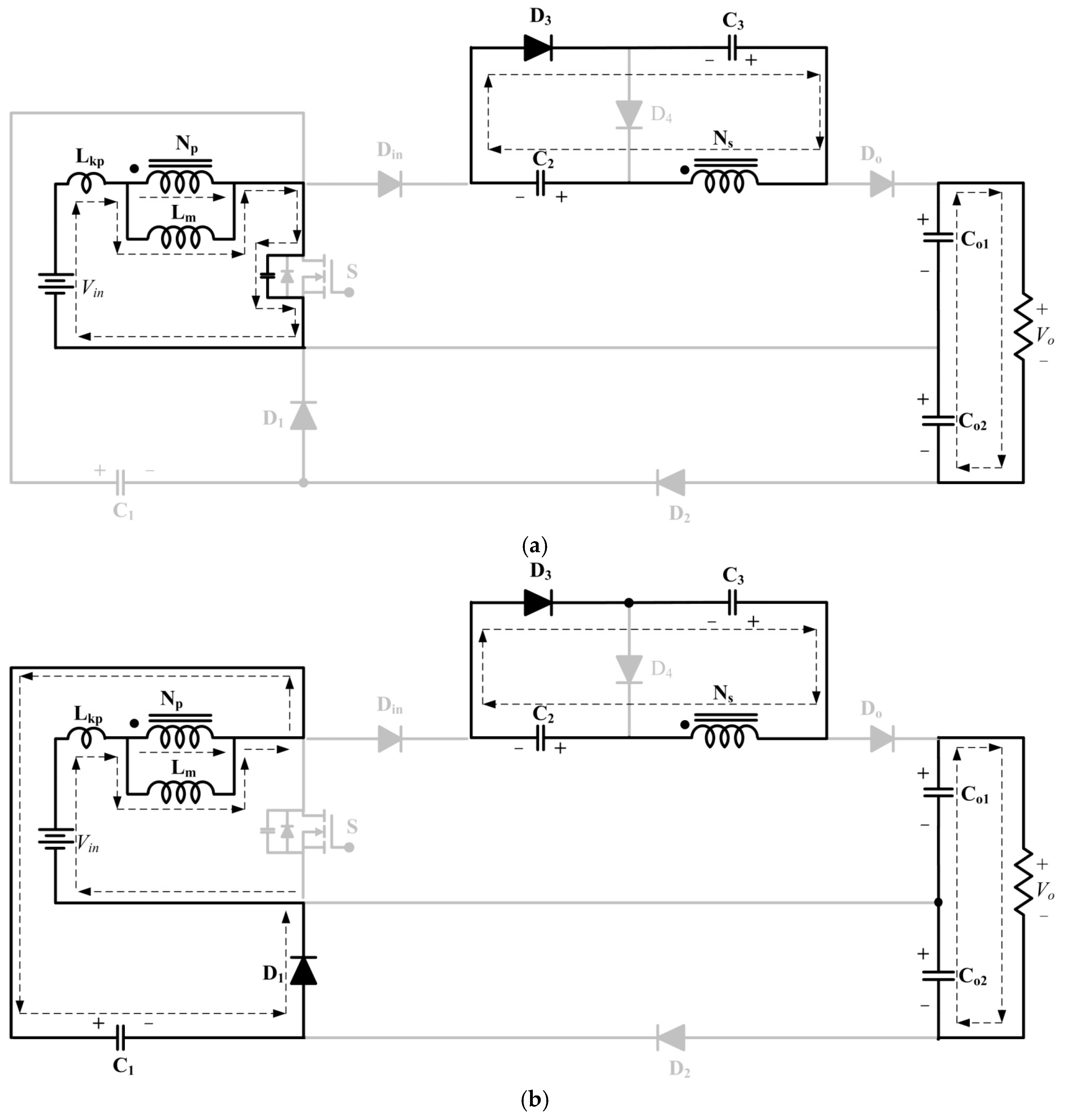
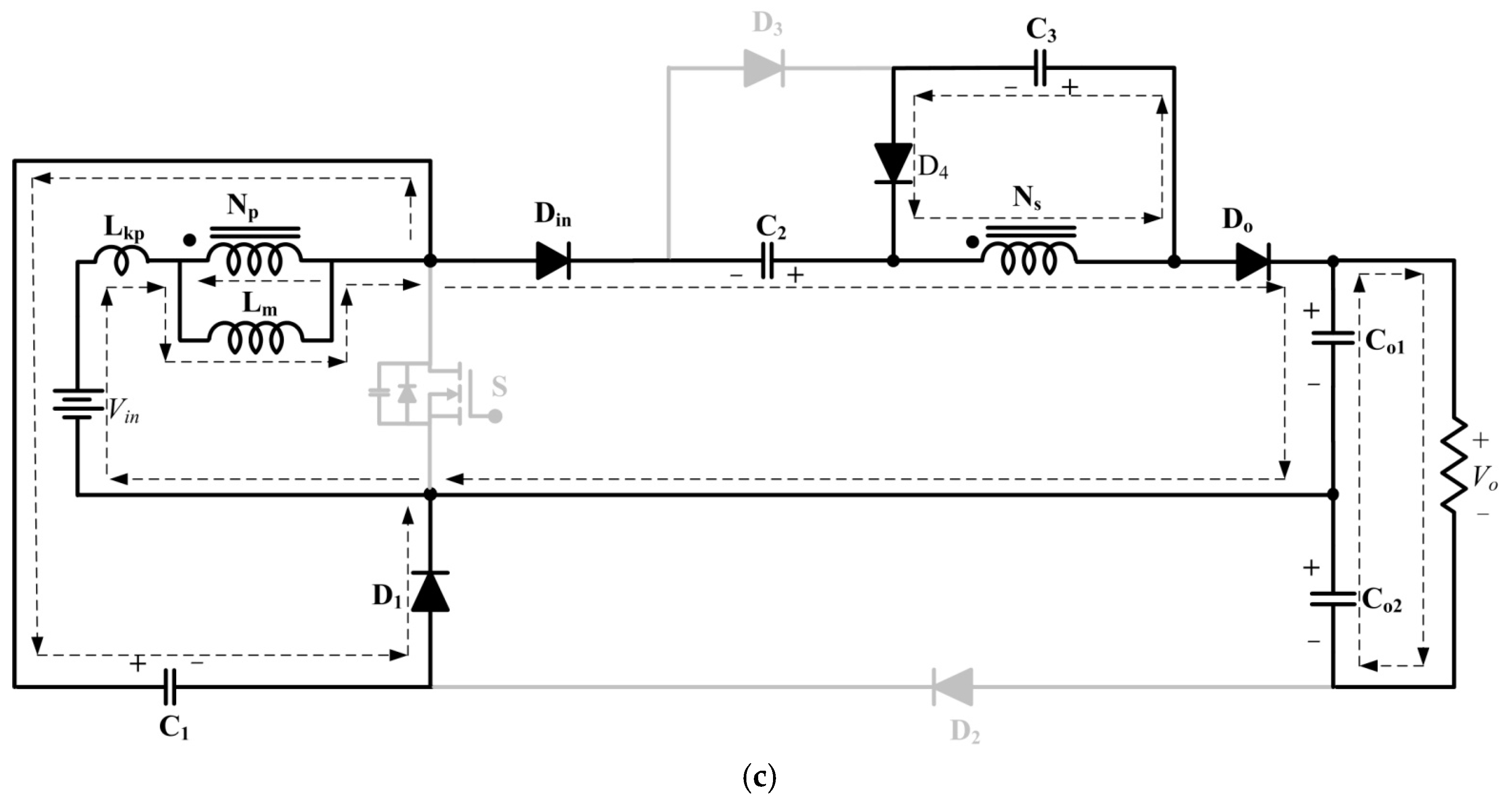
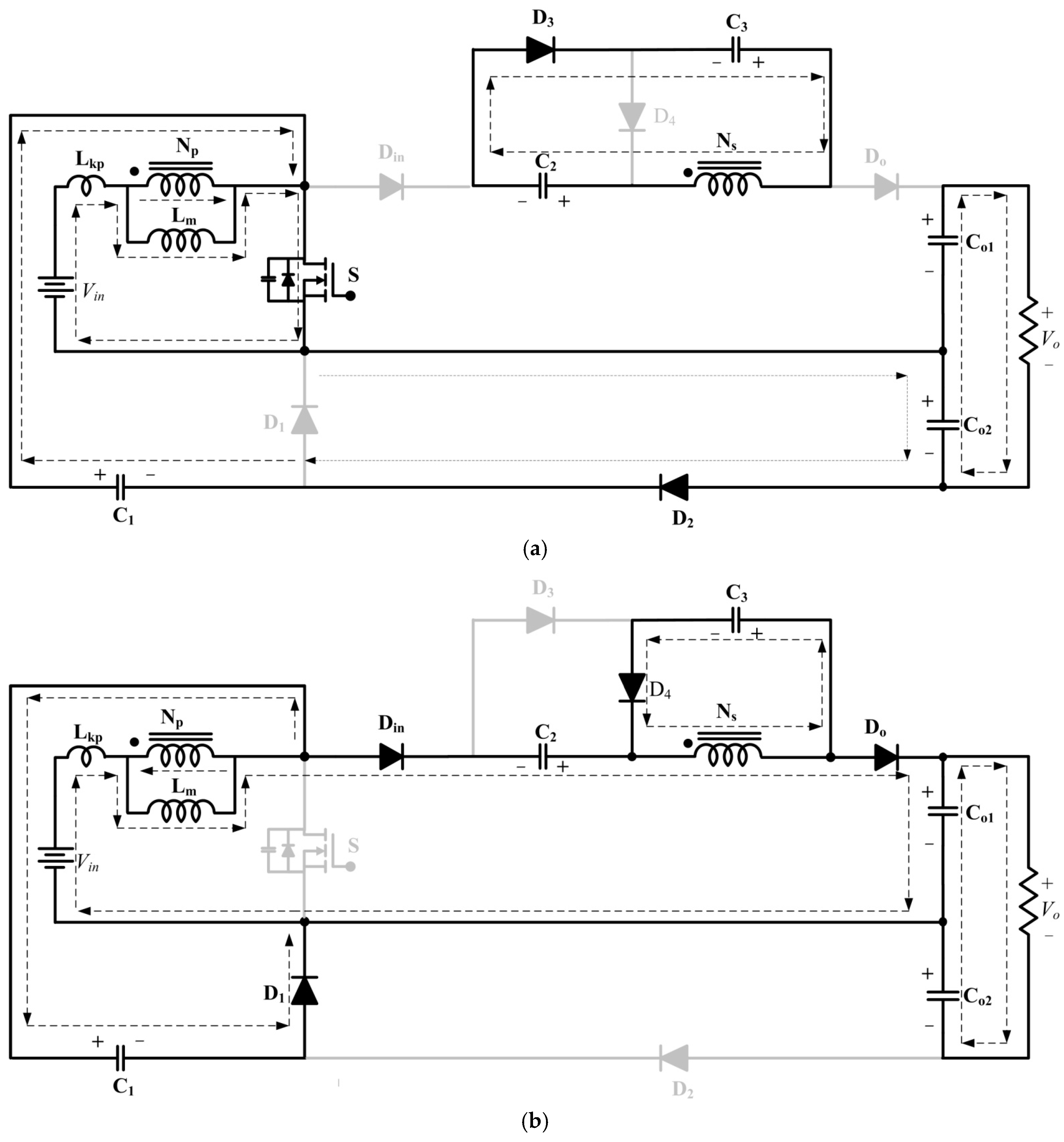
2. Operation Principle of the Proposed Converter

Figure 1 illustrates the proposed converter circuit topology, where the DC input voltage is Vin, main switch is S, and coupled inductors are Np and Ns.
The clamp circuit has two diodes D1 and D2 and a capacitor C1. The step-up circuit has two diodes D3 and D4 and two capacitors C2 and C3. The equivalent circuit of the coupled inductor comprises the leakage inductor Lk, magnetizing inductor Lm, and an ideal transformer with turn numbers Np and Ns of the primary and secondary windings, respectively. To simplify the analysis of the circuit operation principles, the following conditions were assumed:
  • Capacitors C1C3 and Co1Co2 are sufficiently large. Therefore, Vc1Vc3 and Vco1Vco2 are considered constant during an operation.
  • Power devices are ideal components, and the parasitic capacitors of power devices are not neglected.
  • The magnetizing inductance is Lm and leakage inductance is Lk; the coupling coefficient of the coupled inductor is k and is equal to Lm/(Lm+Lk).
  • The turn ratio n is equal to Ns/Np.
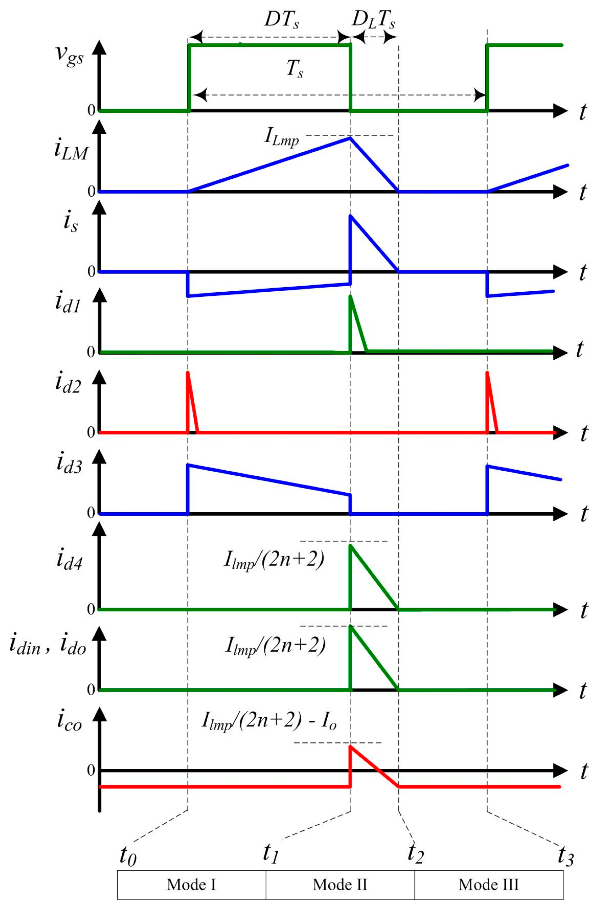
  • The proposed converter operation can be divided into the continuous conduction mode (CCM) and discontinuous conduction mode (DCM). The detail analysis is as follows:
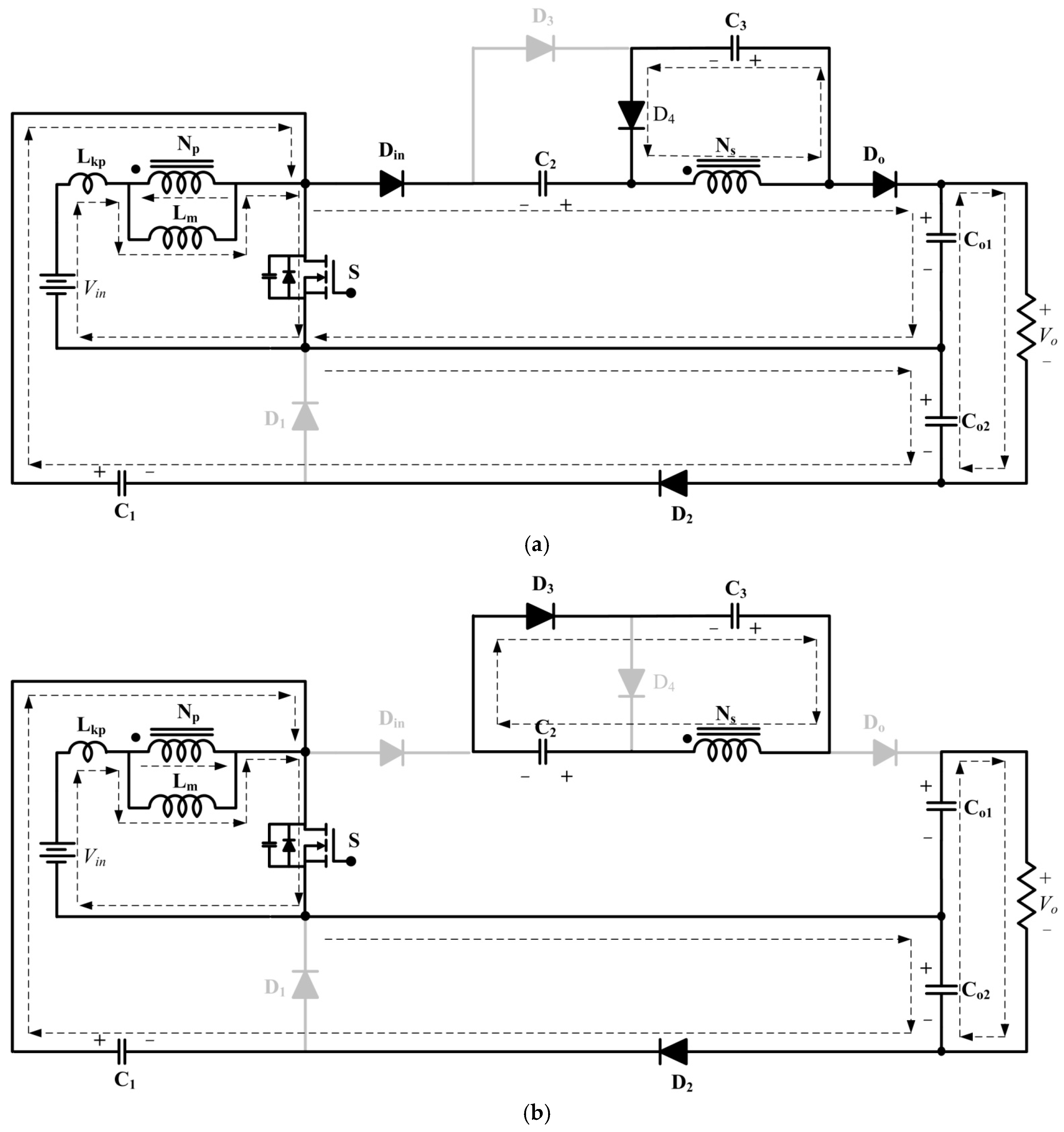
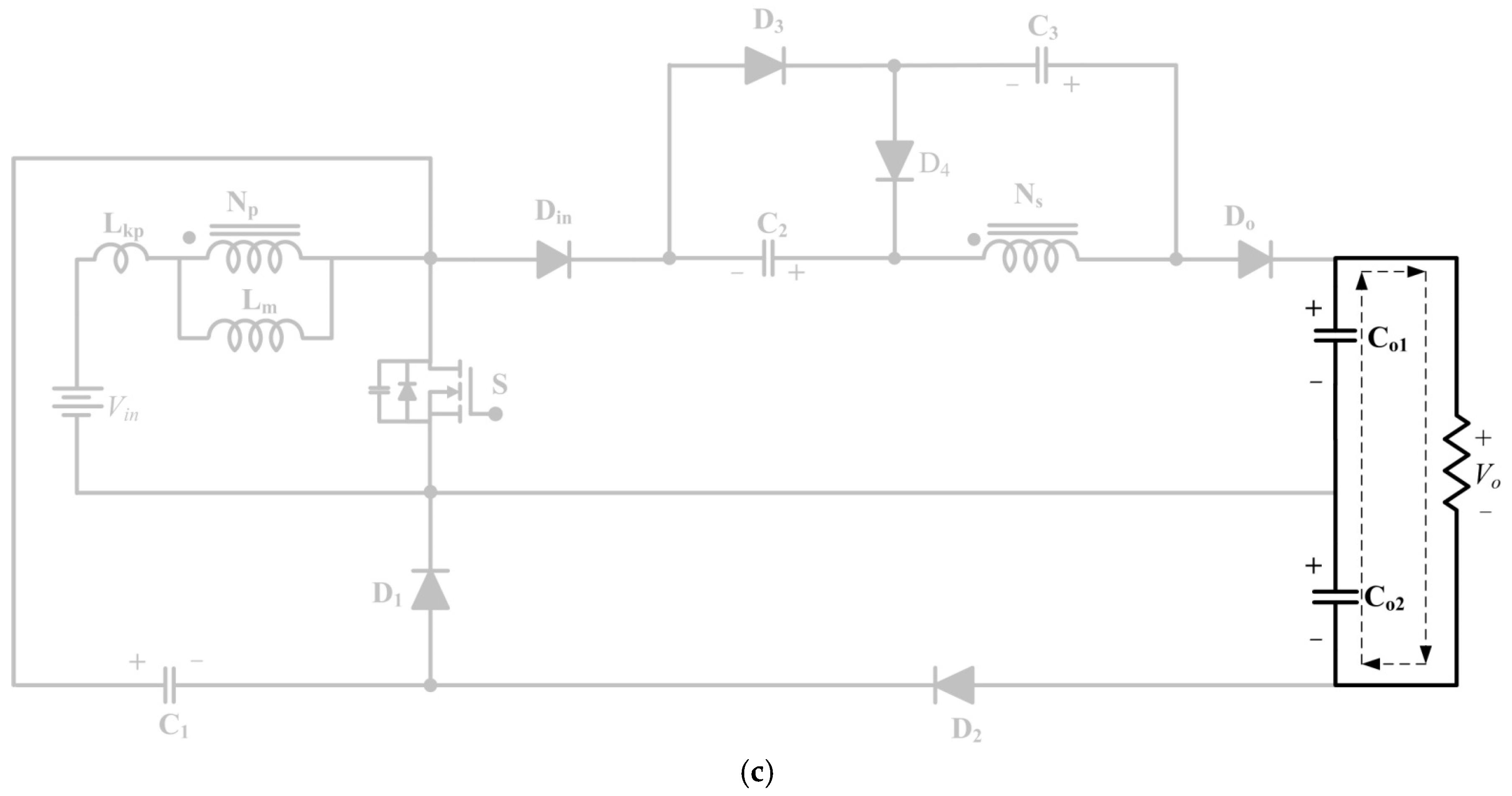
2.1. CCM Operation

Figure 2 shows the main component current and voltage waveforms of the proposed converter during CCM operation.
This CCM operation can be divided into five operating modes as follows:
Mode I [t0, t1]: During this time interval, the power switch S is turned on, and D2, D4, Din, and Do are forward-biased. The equivalent circuit is shown in Figure 3a. The primary-side leakage magnetizing current iLk increases linearly, and the DC source Vin supplies energy to the magnetizing inductor Lm. The secondary-side leakage inductor current is supplies energy to the capacitor C3, and Vc3 is approximately equal to nVL1. The clamp capacitor C1 supplies energy to the high voltage output capacitor Co2. When is equals zero at t = t1, this operation mode is terminated.
Mode II [t1, t2]: The switch S is still turned on, and D3 is forward-biased. The equivalent circuit is shown in Figure 3b. The DC source Vin supplies energy to the magnetizing inductor Lm. The secondary-side capacitor C2 is charged by the coupled inductor and capacitor C3. Vc3 is approximately equal to Vc2nVL1. The output capacitors Co1 and Co2 provide energy to the output load. This operating mode is terminated when the switch S is turned off at t = t2.
Mode III [t2, t3]: At t = t2, the switch S is turned off, and D3 is forward-biased. The equivalent circuit is shown in Figure 4a. The parasitic capacitor Cds of the main power switch S is charged rapidly by the leakage inductor Lk and magnetizing inductor Lm. The secondary-side capacitor C2 is charged by the coupled inductor and capacitor C3. The output capacitors Co1 and Co2 provide energy to the load.
Mode IV [t3, t4]: At t = t3, the switch S is turned off, and D1 and D3 are forward-biased. The equivalent circuit is shown in Figure 4b. The passive clamp capacitor C1 is charged by the leakage inductor Lk and magnetizing inductor Lm; the leakage inductor Lk is recovered and iLk decreases rapidly. The capacitor C2 is charged continuously by the coupled inductor and capacitor C3. This mode is terminated at t = t4 until the secondary-side current is equals zero. Therefore, D3 is turned off and D4, Din, and Do are turned on.
Mode V [t4, t5]: At t = t4, the switch S is turned off, and D1, D4, Din, and Do are forward-biased. The equivalent circuit is shown in Figure 4c. The coupled inductor, DC source Vin, and capacitor C2 are connected to supply energy to the high-output voltage side capacitor Co1 and load. This mode is terminated at t = t5, and the power switch S is turned on again during the next mode.

2.2. DCM Operation

Figure 5 shows the major component current and voltage waveforms of the proposed converter during the DCM operation. To simplify the analysis, the leakage inductor Lk of the coupled inductor is neglected during the DCM operation.
Figure 6 shows the modes I–III operating stages. The operating modes are explained as follows:
Mode I [t0, t1]: During this time interval, the power switch S is turned on, and D2 and D3 are forward-biased. The equivalent circuit is shown in Figure 6a. The primary current iLm increases linearly, and the DC source Vin supplies energy to the magnetizing inductor Lm. The secondary-side coupled inductor in series with the capacitor C3 supplies energy to the capacitor C2. The output capacitors Co1 and Co2 provide energy to the output load. The main switch S is turned off at t = t1, and this operation mode is terminated.
Mode II [t1, t2]: During this time interval, the main switch S is turned off, and D1, D4, Din, and Do are forward-biased. The equivalent circuit is shown in Figure 6b. The magnetizing inductor Lm, DC source Vin, and capacitor C2 are charged by Din and Do and supply energy to the output capacitor Co1. The magnetizing energy of Lm is transferred to capacitor C3 by coupled inductor. This operating mode is terminated when the energy stored in Lm is depleted at t = t2.
Mode III [t2, t3]: During this time interval, the main switch S is turned off. The equivalent circuit is shown in Figure 6c. The output capacitors Co1 and Co2 provide energy to the output load. This mode is terminated at t = t3, and the main switch S is turned on again during the next mode.

3. Steady-State Analysis of the Proposed Converter

3.1. CCM Operation

The turn ratio is defined as:
n = N s N p
The coupling coefficient k of the coupled inductor is defined as:
k = L m L m + L k
Modes I, III, and IV, which have considerably short time durations, are ignored to simplify the steady state analysis; only modes II and V of the CCM operation are considered.
The voltage stresses of VLk, VL1, and VL2 at mode II can be derived on the basis of Figure 3b.
V L k I I = L k 1 L m + L k 1 V i n = ( 1 k ) V i n
V L 1 I I = L m L m + L k 1 V i n = k V i n
V L 2 I I = n V L 1 I I = n k V i n
According to the volt–second balance principle and Lk, Np, and Ns, the following equations are obtained:
0 D T s V L k I I d t + D T s T s V L k V d t = 0
0 D T s V L 1 I I d t + D T s T s V L 1 V d t = 0
0 D T s V L 2 I I d t + D T s T s V L 2 V d t = 0
By substituting (3)–(5) into (6)–(8), the voltage stresses of VLk, VL1, VL2, and Vo at mode V can be expressed as:
V L k V = D ( 1 k ) ( 1 D ) V i n
V L 1 V = D k 1 D V i n
V L 2 V = n D k 1 D V i n
V o = 2 V c 1 + V c 2 V L 2 V
The capacitor C2 is charged in mode II, and the capacitors C1 and C3 are charged in mode V. The voltage stress across capacitors C1, C2, and C3 can be represented on the basis of Figure 3b and Figure 4c.
V c 3 = V L 2 V = n D k 1 D V i n
V c 2 = V L 2 I I + V c 3
By substituting (5) and (13) into (14), the voltage stresses of the capacitors C1 and C2 are expressed as:
V c 2 = n k 1 D V i n
V c 1 = V i n V L k V V L 1 V = ( 1 + D k ( 1 D ) + D ( 1 k ) ( 1 D ) ) V i n
By substituting (11), (15), and (16) into (12), the voltage gain is developed as:
M C C M = V o V i n = 2 + n k + n D k 1 D
Assume k is equal to 1 and neglect the leakage inductor of the coupled inductor. At k = 1, the ideal voltage gain can be derived as:
M CCM = 2 + n + n D 1 D
Table 1 and Figure 7 are shows the voltage gain of the proposed converter and those of previous converters during the CCM operation under coupling coefficient equal to 1. According to this Figure 7, the voltage gain of the proposed converter is higher than those of the previous converters with the same duty cycle. Proposed converter has achieved high step–up ratio and the efficiency of proposed converter is higher than those of the previous converter, except that the converters [9,29]. The converter [9] has high efficiency but voltage stress of the switch is high, the peak voltage of Vds is appropriately 71V during the switch-off period and large coupled inductor size is ETD-59. The low efficiency in converter [29] under 150w and maximum output voltage is 200 V lesser than proposed converter.

3.2. DCM Operation

The DCM operation can be divided into three modes. Figure 5 shows the main component current and voltage waveforms. Figure 6 shows the proposed converter during different modes of the DCM operation. The mode I operation is shown in Figure 6a; the main power switch S is turned on. Therefore, the voltage stresses VL1 and VL2 can be expressed as:
V L 1 I = V i n
V L 2 I = n V i n
The magnetizing inductor peak current can be expressed as:
I L m p = V i n L m D T s
Therefore, the voltage stresses of the capacitors C2, Co1, and Co2 can be expressed as:
V c 2 = V L 2 I + V c 3
V c o 2 = V c 1
V c o 1 = V o V c 1
Figure 6b illustrates the mode II operation; the main power switch S is turned off. Therefore, the voltage stresses during mode II can be expressed as:
V L 1 I I = V i n V c 1
V L 2 I I = 2 V c 1 + V c 2 V o
V L 2 I I = V c 3
Figure 6c illustrates the mode III operation; the main power switch S is turned off. The capacitors Co1 and Co2 supply energy to the load, and the voltage stresses of VL1 and VL2 are expressed as:
V L 1 I I I = V L 2 I I I = 0
By applying the volt–second balance principle to the coupled inductor, the following equations can be obtained:
0 D T s V L 1 I d t + D T s ( D + D L ) T s V L 1 I I d t + ( D + D L ) T s T s V L 1 I I I d t = 0
0 D T s V L 2 I d t + D T s ( D + D L ) T s V L 2 I I d t + ( D + D L ) T s T s V L 2 I I I d t = 0
By substituting (20), (27), and (28) into (30), the voltage across capacitor C3 can be expressed as:
V c 3 = n D D L V i n
Similarly, by substituting (19), (25), and (28) into (29) and (22), (27), and (28) into (30), the stress voltages of capacitors C1 and C2 can be expressed as:
V c 1 = D + D L D L V i n
V c 2 = ( n + n D D L ) V i n
By substituting (20), (26), (28), (32), and (33) into (30), the voltage gain of the proposed converter during the DCM can be expressed as:
V o = [ 2 D D L ( 1 + n ) + ( n + 2 ) ]   V i n
D L = 2 D ( 1 + n ) V i n V o ( 2 + n ) V i n
On the basis of Figure 5, the average current value ico1, can be expressed as:
i c o 1 = 1 2 D L I L m p 2 + 2 n I o
In the steady state, i c o 1 is equal to zero and (21), (35), and i c o 1 = 0 can be substituted into (36). Therefore, (37) can be obtained as:
D 2 ( n + 1 ) V i n 2 T s [ V o ( n + 2 ) V i n ] · ( 2 n + 2 ) · L m = V o R
The time constant of the magnetizing inductance is defined as:
τ L m = def L m R T s
By substituting (38) into (37), the voltage gain can be obtained as follows:
M DCM = V o V i n = 2 n + 2 2 + ( 2 n + 2 ) 2 4 + D 2 ( n + 1 ) ( 2 n + 2 ) · τ L m

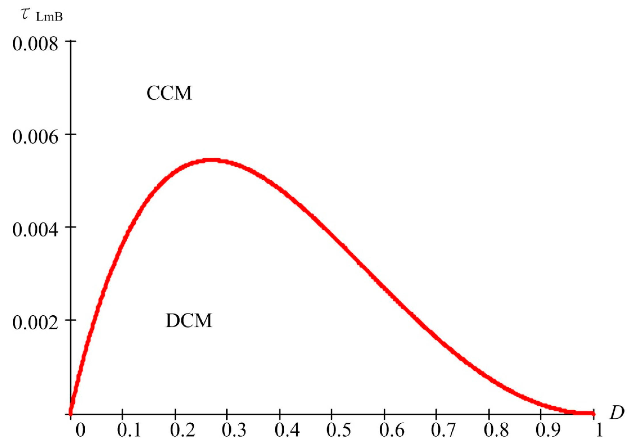
3.3. Boundary Operating Condition between the CCM and the DCM

While operating the proposed converter in boundary-condition mode the voltage gain is equal for CCM and DCM operations. Based on (18) and (39), the time constant τ L m B of the boundary normalized magnetizing inductor can be expressed as:
τ L m B = D 2 ( n + 1 ) 2 n + 2 [ ( 2 + n + n D 1 D ) 2 n + 2 2 ] 2 ( 2 n + 2 ) 2 4
Figure 8 shows the curve of τ . The proposed converter is operated in the CCM when τ is higher than i L m B . Otherwise, the proposed converter is operated in the DCM.

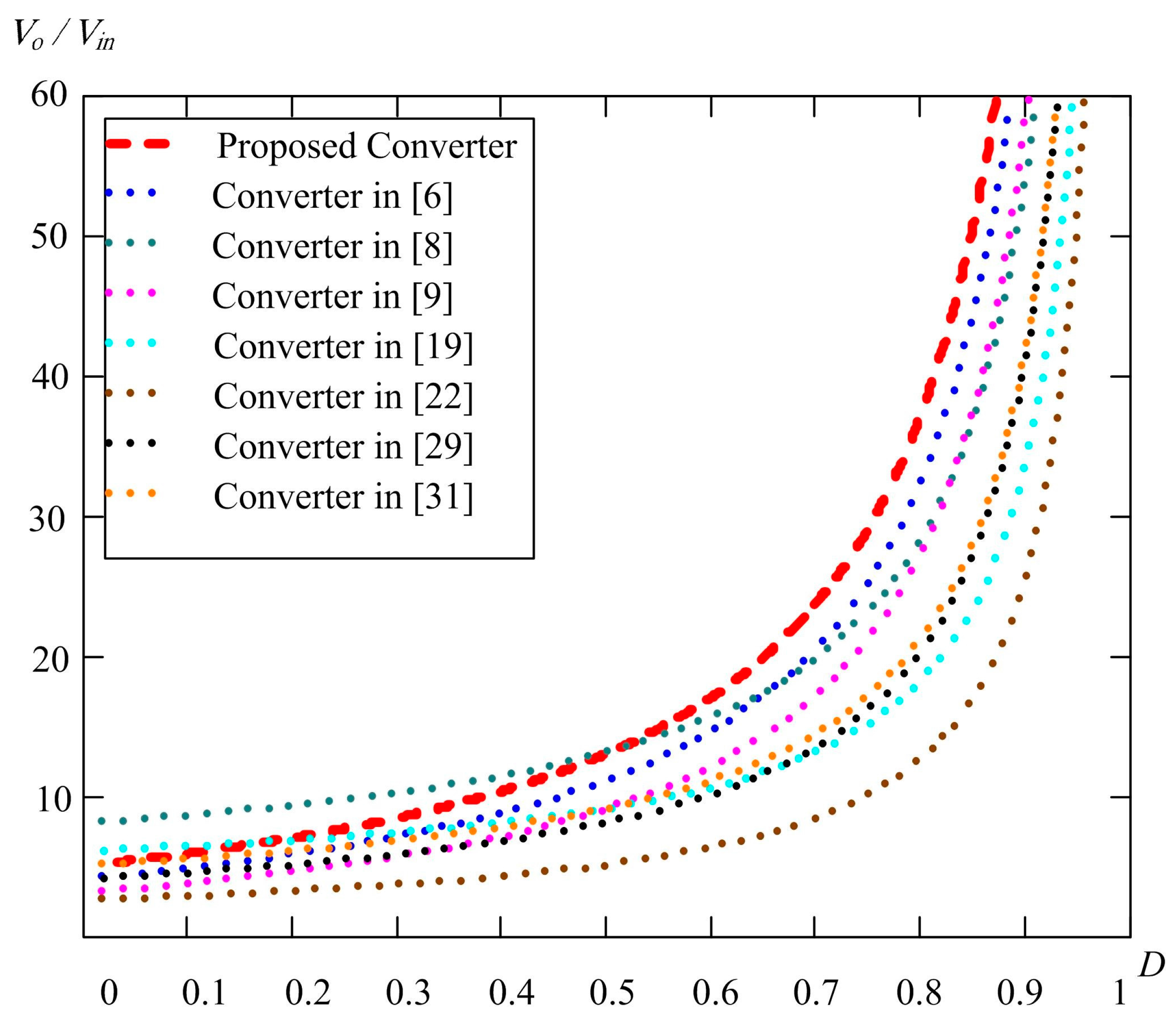
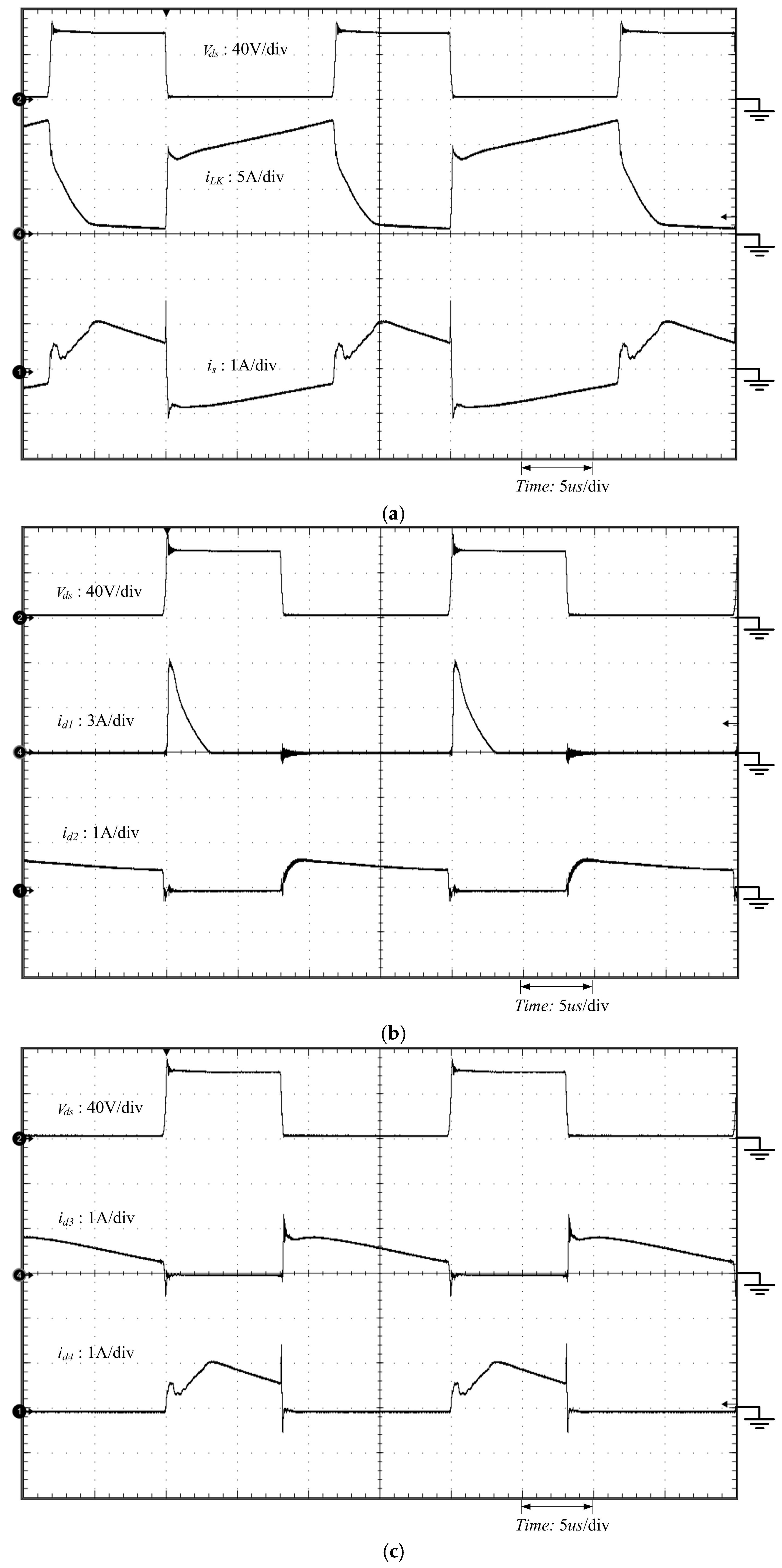
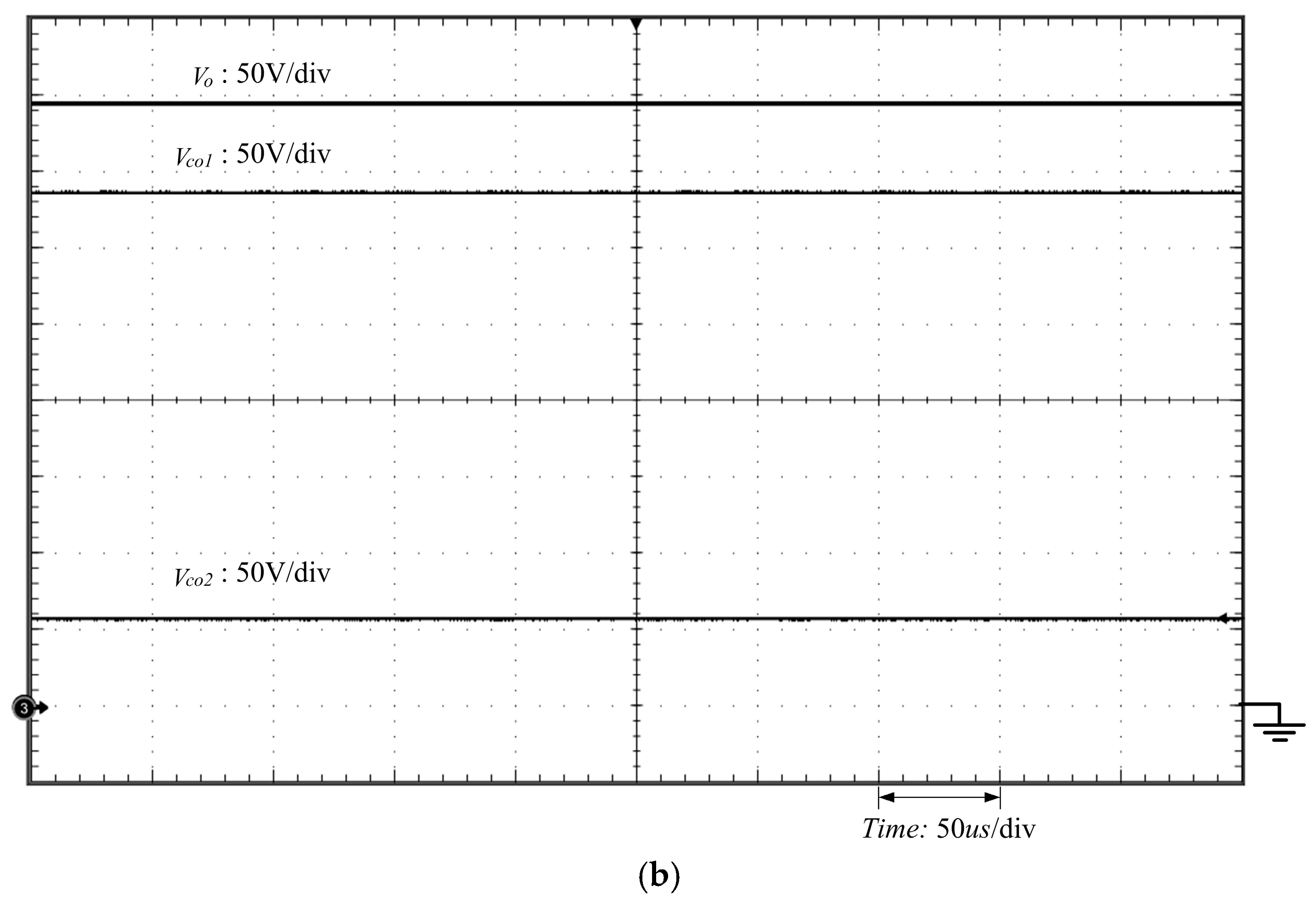
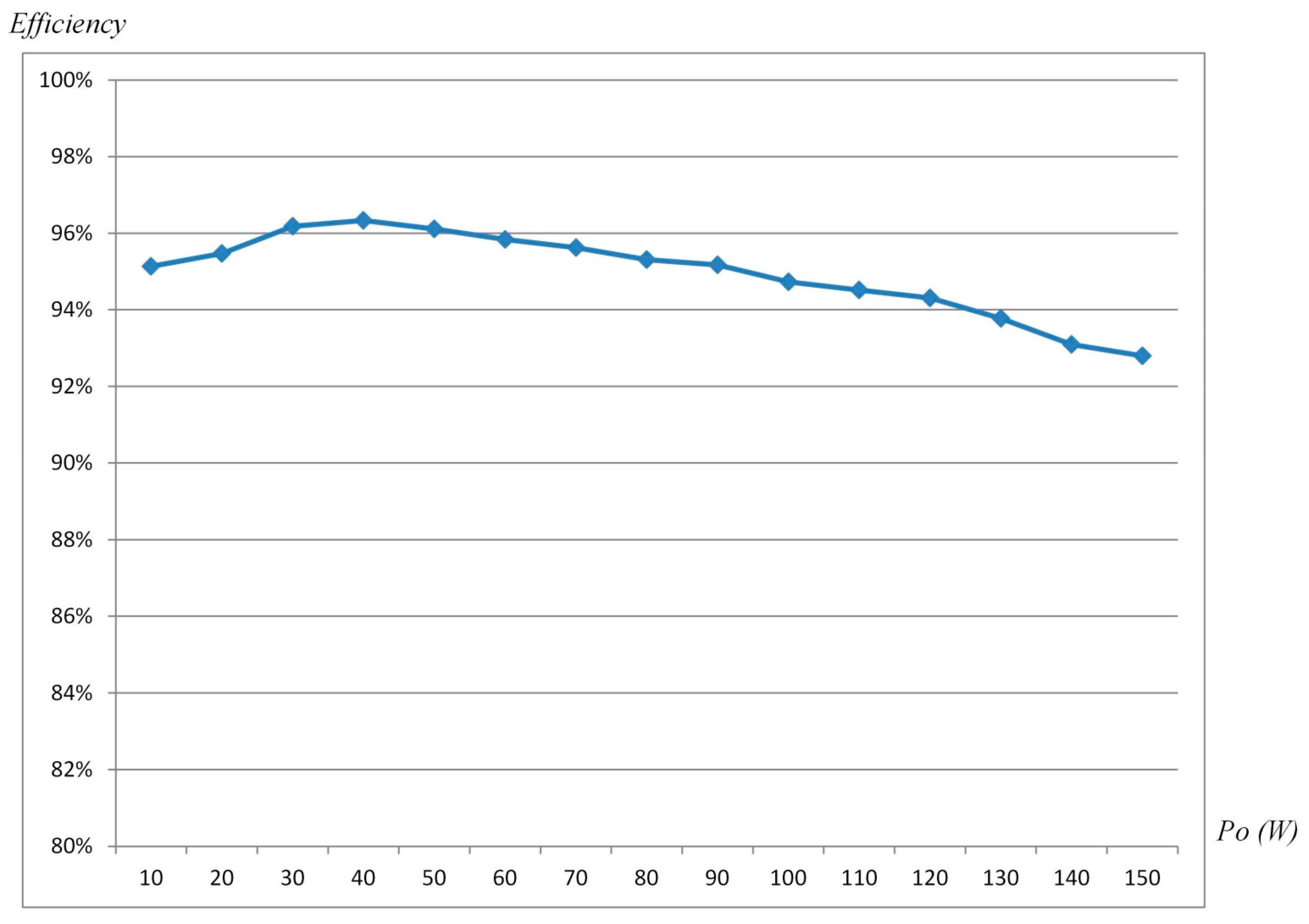
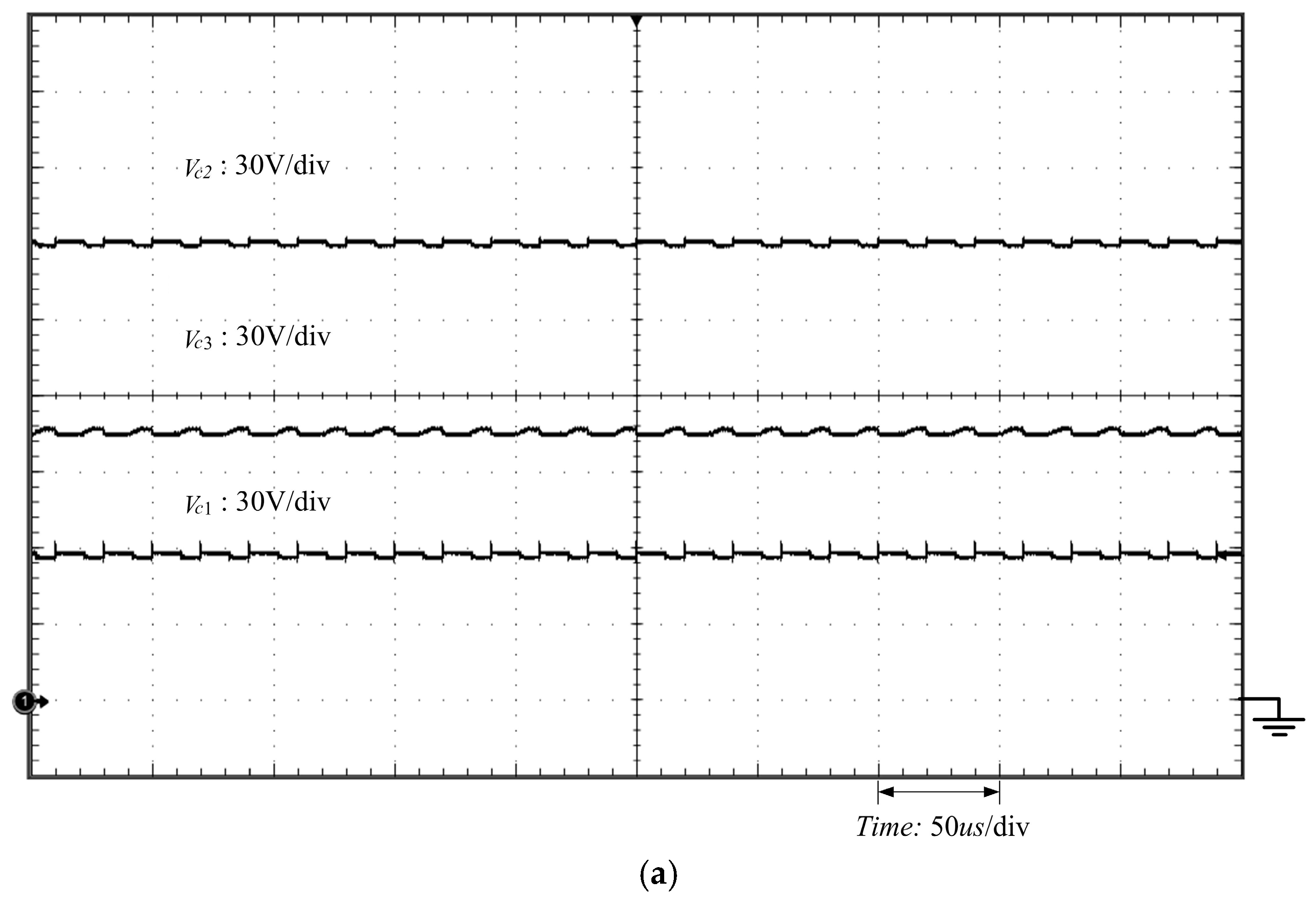
4. Design and Experiment of the Proposed Converter

To test and measure the proposed converter performance, a prototype circuit of the proposed converter at 150 W was constructed in the laboratory. The main specifications are as follows:
  • Input DC voltage V i n : 24 V.
  • Output DC voltage V o : 400   V .
  • Maximum output power: 150 W.
  • Switch frequency: 50 kHz.
  • Switch: IXTH130N10T.
  • Diodes: D1D3, Do: DSEI 30-10A; Din and D4: 25JPE40.
  • Capacitors: C1 and Cco2: 100 μ /100 V, C2: 100 μ /250 V, C3: 100 μ /100 V, and Co1: 220 μ /400 V aluminium capacitors.
  • Transformer: ETD-49 core PC-32, Np:Ns = 1:3, Lm = 32 μH and Lk = 0.22 μH; k = 0.993 .
Figure 9a illustrates the secondary current is, primary-side leakage magnetizing current iLk, and drain to source voltage of the main power switch at full load Po = 150 W and V i n = 24 V. The waveform of the secondary current is of the coupled inductor shows that the proposed circuit does not have zero current when the switch is turned on in the CCM. Figure 9b shows the waveforms of id1 and id2.
The current of the capacitor C1 flows to D2 and energy is transferred to the capacitor Co2 when the switch is turned on. The capacitor C1 absorbs energy from V i n and parasitic capacitor on the switch when the switch is turned off. Figure 9c shows the waveforms of id3 and id4; C2 and C3 are charged by the DC source V i n and secondary-side coupled inductor. Figure 9d shows the waveforms of idin and ido. The energy of V i n though Cin transfers to the step up circuit and current flow to Do and is released to output capacitors.
Figure 10a shows that Vc1, Vc2, and Vc3 satisfy (14), (15), and (17). Figure 10b shows the input and output voltages of capacitors Co1 and Co2. Figure 11 illustrates the efficiency of the proposed converter at 20150 W loads, and the maximum efficiency is 96.2% at 60 W.

5. Conclusions

This study successfully integrated the proposed converter by using the coupled inductor and high step-up circuit. High voltage gain was achieved using the coupled inductor when the capacitor charged and discharged energy. For this paper is integrated coupled inductor and switch capacitor to achieve a high step-up voltage gain without extreme duty cycle. In addition, energy was recovered from the leakage inductor of the coupled inductor by using a passive clamp circuit. The primary-leakage inductor recovered the energy function, and the switch clamp capacitor reduced the voltage spike of the switch. Therefore, when low conducting resistance Rds(on) and low voltage stresses component were selected, the main power switch loss was reduced. Finally, a prototype circuit of the proposed converter with an input voltage of 24 V converted to an output voltage of 400 V and maximum power 150 W was constructed in the laboratory. The experimental results proved the high efficiency and voltage gain of the proposed converter. Moreover, it was proved that the main switch stress voltage is clamped by the capacitor C1.

Acknowledgments

This work were supported in part by the National Synchrotron Radiation Research Center and Ministry of Science and Technology, China, through grant numbers MOST 105-2199-M-006-004 and MOST 104-2221-E-006-073-MY3.

Author Contributions

Yong-Seng Wong and Jiann-Fuh Chen conceived and designed the experiments; Yong-Seng Wong performed the experiments; Yong-Seng Wong, Yi-Ping Hsieh and Jiann-Fuh Chen analyzed the data; Kuo-Bin Liu contributed reagents/materials/analysis tools; Yong-Seng Wong wrote the paper.

Conflicts of Interest

The authors declare no conflict of interest.

References

  1. Anders, L.; Peter, U.C.; Ben, M.; Glenn, A.M.; David, P.; Valentina, R.; Alexander, R. The multimillennial sea-level commitment of global warming. Proc. IEEE Natl. Acad. Sci. USA 2016, 110, 13745–13750. [Google Scholar]
  2. Wei, C.L.; Shih, M.H. Design of a switched-capacitor DC-DC converter with a wide input voltage range. IEEE Trans. Circuits Syst. I 2013, 60, 1648–1656. [Google Scholar] [CrossRef]
  3. Chang, C.H.; Chang, E.C.; Cheng, H.L. A high-efficiency solar array simulator implemented by an LLC resonant DC-DC converter. IEEE Trans. Power Electron. 2013, 28, 3039–3046. [Google Scholar] [CrossRef]
  4. Shen, J.M.; Jou, H.L.; Wu, J.C. Novel transformerless grid-connected power converter with negative grounding for photovoltaic generation system. IEEE Trans. Power Electron. 2012, 27, 1819–1829. [Google Scholar] [CrossRef]
  5. Zhang, L.; Sun, K.; Feng, L.L.; Wu, H.F.; Xing, Y. A family of neutral point clamped full-bridge topologies for transformerless photovoltaic grid-tied inverters. IEEE Trans. Power Electron. 2013, 28, 730–739. [Google Scholar] [CrossRef]
  6. Baek, J.W.; Ryoo, M.H.; Kim, T.J.; Yoo, D.W.; Kim, J.S. High boost converter using voltage multiplier. In Proceedings of the 31st Annual Conference of IEEE Industrial Electronics Society (IECON 2005), Raleigh, NC, USA, 6–10 November 2005; pp. 567–572.
  7. Wai, R.J.; Duan, R.Y. High-efficiency power conversion for low power fuel cell generation system. IEEE Trans. Power Electron. 2005, 20, 847–856. [Google Scholar] [CrossRef]
  8. Hsieh, Y.P.; Chen, J.F.; Liang, T.J.; Yang, L.S. Novel high step-up DC-DC converter for distributed generation system. IEEE Trans. Ind. Electron. 2013, 60, 1473–1482. [Google Scholar] [CrossRef]
  9. Hsieh, Y.P.; Chen, J.F.; Liang, T.J.; Yang, L.S. Analysis and implementation of a novel single-switch high step-up DC-DC converter. IET Power Electron. 2012, 5, 11–21. [Google Scholar] [CrossRef]
  10. Ajami, A.; Ardi, H.; Farakhor, A. A novel high step-up DC/DC converter based on integrating coupled inductor and switched-capacitor techniques for renewable energy applications. IEEE Trans. Power Electron. 2015, 30, 4255–4263. [Google Scholar] [CrossRef]
  11. Luo, F.L.; Ye, H. Positive output multiple-lift push-pull switched-capacitor Luo-converters. IEEE Trans. Ind. Electron. 2004, 51, 594–602. [Google Scholar] [CrossRef]
  12. Abutbul, O.; Gherlitz, A.; Berkovih, Y.; Ioinovici, A. Step-up switching-mode converter with high voltage gain using a switched-capacitor circuit. IEEE Trans. Circuits Syst. I 2003, 50, 1098–1102. [Google Scholar] [CrossRef]
  13. Hsieh, Y.P.; Chen, J.F.; Liang, T.J.; Yang, L.S. Novel high step up DC-DC converter with coupled-inductor and switched-capacitor techniques. IEEE Trans. Ind. Electron. 2012, 59, 998–1007. [Google Scholar] [CrossRef]
  14. Axelrod, B.; Berkovich, Y. Switched coupled-inductor cell for DC-DC converters with very large conversion ratio. IET Power Electron. 2011, 4, 309–315. [Google Scholar]
  15. Duan, R.Y.; Lee, J.D. High-efficiency bidirectional DC-DC converter with coupled inductor. IET Power Electron. 2012, 5, 115–123. [Google Scholar] [CrossRef]
  16. Changchien, S.K.; Liang, T.J.; Chen, J.F.; Yang, L.S. Step-up DC-DC converter by coupled inductor and voltage-lift technique. IET Power Electron. 2013, 3, 369–378. [Google Scholar] [CrossRef]
  17. Hsieh, Y.P.; Chen, J.F.; Yang, L.S.; Wu, C.Y.; Liu, W.S. High-conversion-ratio bidirectional DC-DC converter with coupled inductor. IEEE Trans. Ind. Electron. 2014, 61, 210–222. [Google Scholar] [CrossRef]
  18. Zhao, Q.; Lee, F.C. High-efficiency, high Step-up DC-DC converters. IEEE Trans. Power Electron. 2003, 18, 65–73. [Google Scholar] [CrossRef]
  19. Lee, J.H.; Liang, T.L.; Chen, J.F. Isolated coupled-inductor-integrated DC-DC converter with nondissipative snubber for solar energy applications. IEEE Trans. Ind. Electron. 2014, 61, 3337–3348. [Google Scholar] [CrossRef]
  20. Hsieh, Y.P.; Chen, J.F.; Liang, T.J.; Yang, L.S. Novel high step-up DC-DC converter with coupled-inductor and switched-capacitor techniques for a sustainable energy system. IEEE Trans. Power Electron. 2011, 26, 3481–3490. [Google Scholar] [CrossRef]
  21. Siwakoti, Y.P.; Blaabjerg, F.; Loh, P.C. Ultra-step-up DC-DC converter with integrated autotransformer and coupled inductor. In Proceedings of the 2016 IEEE Applied Power Electronics Conference and Exposition (APEC), Long Beach, CA, USA, 20–24 March 2016; pp. 1872–1877.
  22. Liang, T.J.; Lee, J.H.; Chen, S.M.; Chen, J.F.; Yang, L.S. Novel isolated high step-up DC-DC converter with voltage lift. IEEE Trans. Power Electron. 2013, 60, 1483–1491. [Google Scholar] [CrossRef]
  23. Chen, Y.T.; Tsai, M.H.; Liang, R.H. DC-DC converter with high voltage gain and reduce switch stress. IET Power Electron. 2014, 7, 2564–2571. [Google Scholar] [CrossRef]
  24. Lin, B.R.; Dong, J.Y. Analysis and implementation of an active clamping zero-voltage turn-on switching/zero-current turn-off switching converter. IET Power Electron. 2010, 3, 429–437. [Google Scholar] [CrossRef]
  25. Zhao, Q.; Tao, F.; Hu, Y.; Lee, F.C. Active-clamp DC/DC converters using magnetic switches. In Proceedings of the Sixteenth Annual IEEE Applied Power Electronics Conference and Exposition (APEC 2001), Anaheim, CA, USA, 4–8 March 2002; pp. 946–952.
  26. Tseng, K.C.; Liang, T.J. Analysis of integrated boost-flyback step-up converter. IEEE Proc. Inst. Elect. Eng. Electric. Power Appl. 2005, 151, 217–225. [Google Scholar]
  27. Wai, R.J.; Duan, R.Y.; Jheng, K.H. High-efficiency bidirectional DC-DC converter with high-voltage gain. IET Power Electron. 2012, 5, 173–184. [Google Scholar] [CrossRef]
  28. Kuo, P.H.; Liang, T.J.; Tseng, K.C.; Chen, J.F.; Chen, S.M. An isolated high step-up forward/flyback active-clamp converter with output voltage lift. In Proceedings of the 2010 IEEE Energy Conversion Congress and Exposition (ECCE), Atlanta, GA, USA, 12–16 September 2010; pp. 542–548.
  29. Wai, R.J.; Liu, L.W.; Duan, R.Y. High-efficiency voltage-clamped DC-DC converter with reduced reverse-recovery current and switch-Voltage stress. IEEE Trans. Ind. Electron. 2006, 53, 272–280. [Google Scholar]
  30. Wu, T.F.; Lai, Y.S.; Hung, J.C.; Chen, Y.M. Boost converter with coupled inductors and buck-boost type of active clamp. IEEE Trans. Ind. Electron. 2008, 55, 154–162. [Google Scholar] [CrossRef]
  31. Wai, R.J.; Lin, C.Y.; Duan, R.Y.; Chang, Y.R. High-efficiency DC-DC converter with high voltage gain and reduced switch stress. IEEE Trans. Ind. Electron. 2007, 54, 354–364. [Google Scholar] [CrossRef]
  32. Muhammad, M.; Armstrong, M.; Elgendy, M.A. A nonisolated interleaved boost converter for high-voltage gain applications. IEEE J. Emerg. Sel. Top. Power Electron. 2016, 4, 352–362. [Google Scholar] [CrossRef]
  33. Muhammad, M.; Armstrong, M.; Elgendy, M. Non-isolated DC-DC converter for high-step-up ratio applications. In Proceedings of the 2015 17th European Conference on Power Electronics and Applications (EPE'15 ECCE-Europe), Geneva, Switzerland, 8–10 September 2015; pp. 1–10.
  34. Muhammad, M.; Armstrong, M.; Elgendy, M.A. Non-isolated, high gain, boost converter for power electronic applications. In Proceedings of the 8th IET International Conference on Power Electronics, Machines and Drives (PEMD 2016), Glasgow, UK, 19–21 April 2016.
Figure 1. Circuit configuration of the proposed converter.
Energies 10 00378 g001
Figure 2. Key components current and voltage waveforms of the proposed converter at CCM.
Energies 10 00378 g002
Figure 3. Operating modes at CCM during a switching period (Switch turn on). (a) Modes I; (b) Modes II.
Energies 10 00378 g003
Figure 4. Operating modes at CCM during a switching period (Switch turn off). (a) Modes III; (b) Modes IV; and (c) Modes V.
Energies 10 00378 g004aEnergies 10 00378 g004b
Figure 5. Key components current and voltage waveforms of the proposed converter at DCM operation.
Energies 10 00378 g005
Figure 6. Operating modes at DCM during a switching period. (a) Modes I; (b) Modes II; and (c) Modes III.
Energies 10 00378 g006aEnergies 10 00378 g006b
Figure 7. Duty ratio versus voltage gain of the proposed converter compared with previous converters, condition is CCM operation under k = 1 and n = 3 .
Energies 10 00378 g007
Figure 8. Duty ratio versus τ L m B at boundary condition of the proposed converter under n = 3.
Energies 10 00378 g008
Figure 9. Experiment waveform under full-load Po = 150 W. (a) Measured waveforms of Vds, iLk and is; (b) Measured waveforms of Vds, id1 and id2; (c) Measured waveforms of Vds, id3 and id4; and (d) Measured waveforms of Vds, idin and ido.
Energies 10 00378 g009aEnergies 10 00378 g009b
Figure 10. Experiment waveform under full-load Po = 150 W. (a) Measured waveforms of v1, v2 and v3; (b) Measured waveforms of Vco1, Vco2 and Vo.
Energies 10 00378 g010aEnergies 10 00378 g010b
Figure 11. Efficiency of proposed converter.
Energies 10 00378 g011
Table 1. Comparison of the proposed converter compared with some of the previous converters. NA: Not showing efficiency in reference paper.
ConvertersNo. of ComponentsEfficiencyVin/VoutVoltage Gain ( M CCM = Vo/Vin)
proposed converter6 diodes,96.20%Vin = 24 V, M CCM = 2 + n + n D 1 D
5 capacitorsVo = 400 V
[6]3 diodes,NAVin = 48 V, M CCM = 1 + n 1 D
3 capacitorsVo = 380 V
[8]4 diodes,95.88%Vin = 24 V, M CCM = 1 + n + n D 1 D
4 capacitorsVo = 400 V
[9]4 diodes,96.70%Vin = 24 V, M CCM = 2 + n 1 D + n
4 capacitorsVo = 400 V
[19]5 diodes,95.70%Vin = 24 V, M CCM = n 1 + D 1 D
4 capacitorsVo = 200 V
[22]5 diodes,96.20%Vin = 24 V, M CCM = n ( 2 D ) 1 D
3 capacitorsVo = 200 V
[29]5 diodes,96.50%Vin = 27–37.5 V, M CCM = 2 + n 2 ( 1 D )
3 capacitorsVo = 200 V
[31]3 diodes,95.20%Vin = 27–36.5 V, M CCM = ( 1 + n ) + 1 1 D + D 1 D n
3 capacitorsVo = 200 V

