
Space Vector Modulation for an Indirect Matrix Converter with Improved Input Power Factor

Faculty of Electrical and Electronics Engineering, Ho Chi Minh City University of Technology, VNU-HCM Ho Chi Minh City 700000, Vietnam
*
Author to whom correspondence should be addressed.
Energies 2017, 10(5), 588; https://doi.org/10.3390/en10050588
Submission received: 16 February 2017
/
Revised: 17 April 2017
/
Accepted: 19 April 2017
/
Published: 25 April 2017
(This article belongs to the Special Issue Power Electronics and Power Quality)
Abstract
:Pulse width modulation strategies have been developed for indirect matrix converters (IMCs) in order to improve their performance. In indirect matrix converters, the LC input filter is used to remove input current harmonics and electromagnetic interference problems. Unfortunately, due to the existence of the input filter, the input power factor is diminished, especially during operation at low voltage outputs. In this paper, a new space vector modulation (SVM) is proposed to compensate for the input power factor of the indirect matrix converter. Both computer simulation and experimental studies through hardware implementation were performed to verify the effectiveness of the proposed modulation strategy.
1. Introduction
Matrix converters (MCs) provide a number of advantages, including sinusoidal input and output currents, regeneration capability, and compact size with good power-to-weight ratio. The development of MCs began in the early 1980s when Alensia and Venturini introduced the basic principles of operation [1]. Afterwards, the MCs were applied to the adjustable motor speed drive, for renewable energy applications, power supplies, and many others application [2,3].
MCs are classified into direct matrix converters (DMCs) and indirect matrix converters (IMCs) [4]. Both converters are able to generate input/output waveforms with the same performance and the same voltage transfer ratio capability. The IMC is now preferable to the DMC because it has many extra advantages over the DMC, such as easy implementation, more secure computation, the possibility power switch number reduction, and the possibility of constructing AC-AC converters with multiple three-phase outputs and multiphase output voltages [5,6,7].
The modulation strategies for IMC have recently been discussed, and many researchers have developed various methods for IMC modulation. In [8], space vector modulation (SVM) methods were proposed for common mode voltage reduction. In order to reduce the harmonic level in the load side, a new modulation method based on the virtual DC-link voltage was applied [9]. However, the analysis of the input power factor of the IMC has not been presented in the literature.
Figure 1 shows the main circuit of the IMC. The IMC system consists of an input LC filter, a rectifier stage, and an inverter stage. In Figure 1, the LC input filter, which consists of three inductors and three capacitors, acts as an interface between the power supply and converter, so that it smoothens the input currents, and removes the electromagnetic interference (EMI) problems. However, it diminishes the power factor at the input power supply, and the input power factor cannot be unified anymore. Particularly, in the case of operation at low voltage output, the input power factor is greatly worsened. It is well known that the poor input power factor induces negative effects on AC power source utilization, as well as increasing the magnitude of the electric current more than is necessary.
In case of the conventional space vector modulation method for the IMC, the input sectors and the duty cycles of the modulated switches in the rectifier stage are determined by the input phase voltage magnitude and its phase angle [5,6,7,8,9]. Although there is much work required to ensure good performance on the output voltage and input current by the IMC with the conventional SVM, papers investigating the input power factor problem are rare.
In this paper, we propose a new SVM method for the IMC, which can easily compensate for the input power factor without IMC performance degradation. The compensation algorithm is based on the calculation of the optimal compensation angle, which depends on input filter parameters and the demanded output load.
This paper is organized as follows: The IMC operation and the conventional SVM method are presented in Section 2. The effects of the input filter in the input side and the proposed SVM method are described in Section 3. The simulation and experimental results are provided in Section 4 and Section 5, respectively. Some conclusions are given in the last section.
2. Operational Principles of IMC and Conventional SVM Method
2.1. Operational Principles of IMC
The power circuit of the IMC feeding a three-phase inductive load is shown in Figure 1. The voltages and currents at the power supply side are denoted by (va, vb, vc) and (ia, ib, ic), respectively, while those of the load side are denoted by (vA, vB, vC) and (iA, iB, iC). The IMC consists of two stages, i.e., rectifier stage and inverter stage, as shown in Figure 1. The purpose of the rectifier stage is to generate a sinusoidal input current, as well as the positive DC-link voltage. The rectifier stage successively connects the positive input voltage to the positive pole (p), and the negative voltage to the negative pole (n) of DC-link bus. Based on DC-link voltage, which is determined by segment of two positive line-to-line input voltages, the inverter stage is modulated to generate the three-phase output voltage with the desired magnitude and variable frequency.
2.2. Conventional SVM Method
In the conventional SVM approach for the IMC, the operation of the rectifier stage depends only on the phase angle and instantaneous value of the input voltage. The balanced three–phase input voltage is given in Equation (1).
where Vin is the input voltage magnitude and ωin is the input angular frequency.
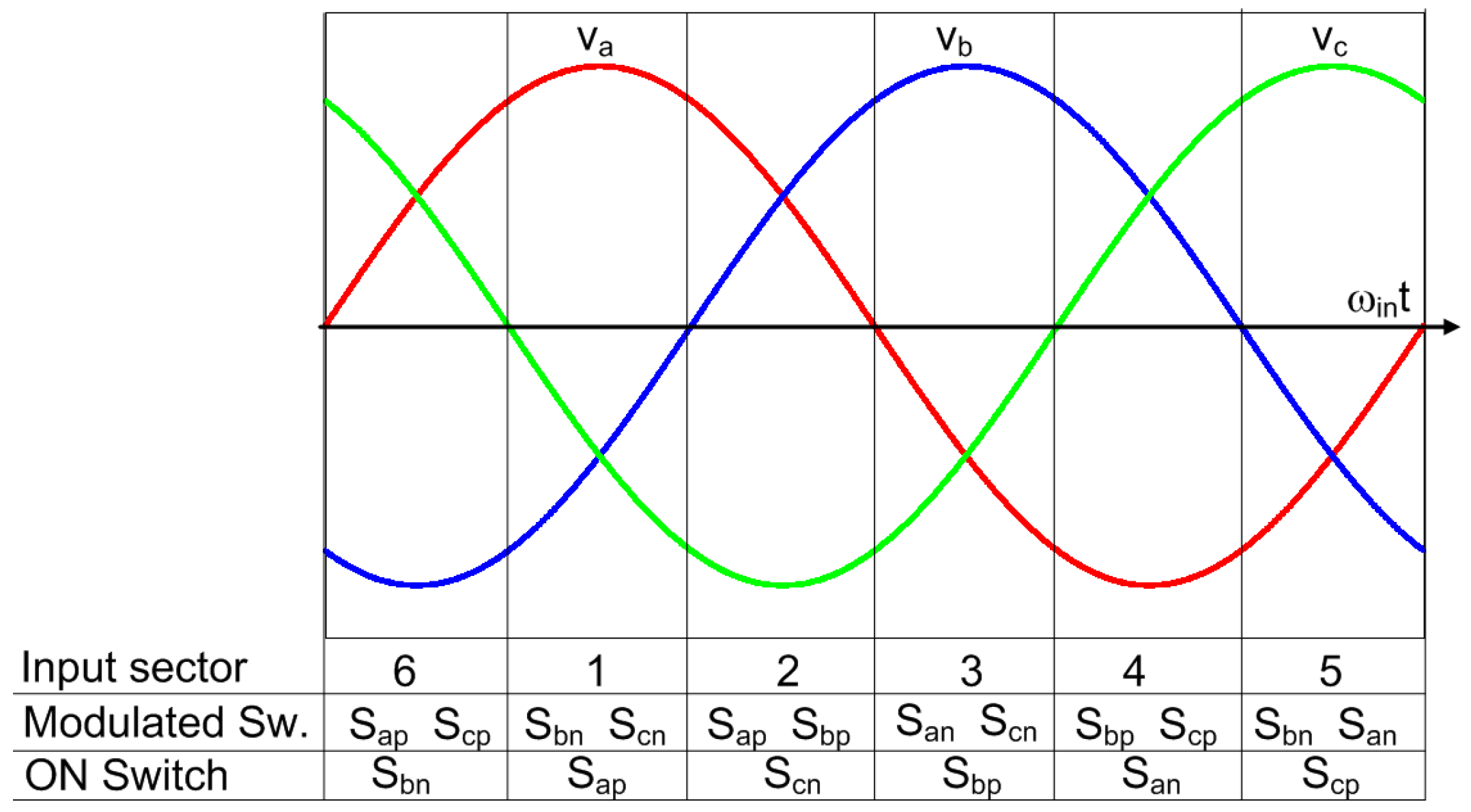
From the input voltage, the input sectors are defined as shown in Figure 2. The six input sectors shown in Figure 2 can be classified into two cases: In the first case, one input voltage is positive and two input voltages are negative (sectors 1, 3, 5). In the second case, two input voltages are positive and one input voltage is negative (sectors 2, 4, 6).
To explain easily how to find the duty cycle of all switches in the rectifier stage, for example, we assume that the rectifier stage operates in sector 1 without missing the generality of the analysis. In this sector, the instantaneous supply voltage va is positive, while vb and vc are negative. Under this condition, the switch Sap is always on while Sbn and Scn are modulated. Based on the analysis in [5,6,7,8,9], the duty cycle of two switches Sbn and Scn are given as:
During one sampling period, the DC-link voltage is modulated with two line-to-line input voltages; while Sbn is turned on, the DC-link voltage equals to vab, and while Scn is turned on, the DC-link voltage equals to vac.
The average DC-link voltage is obtained as follows:
From Equation (4), the minimum value of the average DC-link voltage is
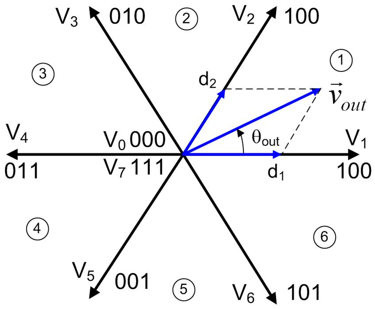
We can find the switching states, the corresponding DC-link voltage, and its average value for any other input sector, by utilizing the same approach, and the results are summarized in Table 1. Once the switching state of the rectifier stage is determined, the traditional space vector pulsewidth modulation (SVPWM) can be applied to control the inverter stage. For calculating the duty cycles of the active and zero vectors in the inverter stage, it is necessary to refer to the local average DC-link voltage value. The eight space vectors with the six active vectors (V1~V6) and the two zero vectors (V0, V7) are used in the SVPWM method.
For a reference output voltage vector, , with the magnitude, Vout, and the phase angle, θout, in sector 1 shown in Figure 3, the duty cycles of two active vectors V1, V2 and two zero vectors V0, V7 are given as follows:
where d0, d1, d2 and d7 are duty cycles of V0, V1, V2 and V7, respectively.
The voltage transfer ratio of the IMC, m, is defined as follows:
According to Equations (4)–(7), the voltage transfer ratio should be smaller than 0.866 in order to maintain all duty cycles positive.
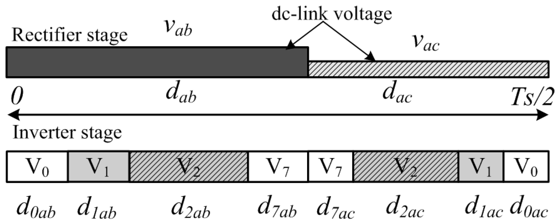
To obtain the balanced input current and output voltage, the switching patterns for the rectifier and the inverter stage should be combined effectively. As mentioned before, the DC-link voltage has two values, vab and vac, during one sampling period with the duty cycles dab and dac, respectively. Therefore, the switching states at the inverter stage are divided into two groups, as shown in Figure 4. The duty cycles of two active and two zero vectors in each group are calculated as follows:
3. SVM to Compensate Input Power Factor
3.1. Input Filter Analysis
Figure 5 shows the equivalent circuit of the input filter per phase: va and ia are the voltage and current of the power supply, vai, and iai are the rectifier input voltage and current after the filter. The equivalent single-phase model in Figure 5 can be used to derive the displacement angle between the source line current ia and the input voltage va [10].
From Figure 5, it follows:
Therefore, the input current and voltage can be rewritten as:
Hence, the input filter causes the phase angle difference between the voltage and current of the power source, which is given as:
where Vin, Iin are the input voltage and the current amplitude of the power supply, respectively. L and C are the inductance and capacitance of the input filter.
In this paper, we consider a new SVM method to compensate the displacement angle between the input current and the voltage in Equation (12).
3.2. The proposed SVM Method
For convenience, the input space vectors are defined as follows:
where and are the input current and the input voltage space vectors, respectively.
Table 2 shows the entire possible switching states and the corresponding space vectors for input current. From Table 2, the input current space vectors are composed of six active current vectors with fixed directions and three zero vectors, where Idc refers to the DC-link current. Figure 6 shows the space vector diagram of the rectifier stage. Each active current vector represents the switching condition between the input phase voltage and the DC-link bus.
In order to compensate for the displacement angle caused by the input filer, the input current vector has to be lagged behind the input voltage vector with the angle δ as shown in Figure 6. If we assume that the input current space vector, Iin, is located in sector 1, Iin is synthesized by two neighbor active vectors Iab and Iac. The duty cycles dδ and dγ for two active vectors are given by:
where mrec is the modulation index of the rectifier stage.
In the modulation of the rectifier stage, the zero current vectors are not used to obtain the maximum DC-link voltage.
Therefore, in order to complete the sampling period, the duty cycles of two adjacent active vectors are adjusted as follows:
And, the average DC-link voltage becomes:
The calculation of duty cycles for the active and zero vectors is similar to that of the conventional method, and they are given in Equation (20).
Similar to the conventional method, the voltage space vectors in the inverter stage are arranged in a double-side switching sequence V0–V1–V2–V7–V7–V2–V1–V0, but with unequal halves.
The duty cycles of the active and the zero vectors in the inverter stage are given in Equation (21) during which the first active current vector Iab is applied to the rectifier stage.
In contrary, when the second active current vector Iac is applied to the rectifier stage, the duty cycles are obtained as Equation (22).
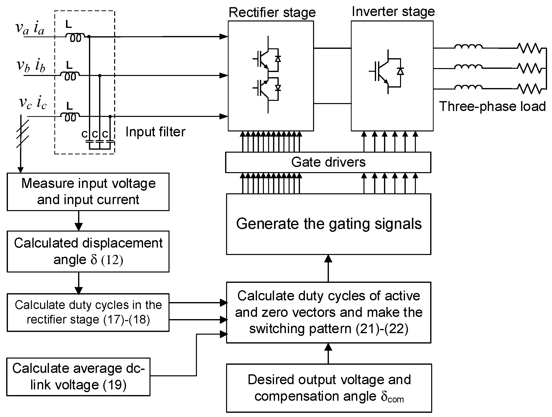
Figure 7 shows the block diagram of the proposed SVM method. First, after detecting the three-phase input voltages/currents using voltage/current sensors, the displacement angle δ is calculated based on Equation (12). Then, the duty cycles of the active vectors in the rectifier stage and average dc-link voltage are determined based on Equations (18) and (19). In the inverter stage, the duty cycles of active and zero vectors are calculated based on the desired output voltage, desired compensation angle δcom, and the duty cycles of the rectifier stages. Finally, the gating signals are generated by using the switching pattern.
From Equation (1) and Figure 6, the line-to-line input voltages vab and vac are obtained as follows:
From Equation (23)–(25), in order to keep vab and vac positive, the compensation angle should satisfy the Equation (26).
Therefore, the compensation angle is chosen as following:
4. Simulation Results
In order to verify the performance and the effectiveness of the proposed method, simulations were carried out using Psim 9.0 software (Powersim Inc., Rockville, MD, USA) with three-phase RL load. The parameters of the IMC system were as follows:
- Three-phase load: R = 12 Ω, L = 10 mH.
- Input filter inductance: L = 1 mH, input filter capacitance: C = 25 µF.
- Switching frequency: 10 kHz (Ts = 100 μs).
- Three-phase power supply voltage for the IMC set to 100 V (line-to-neutral voltage), frequency: 60 Hz.
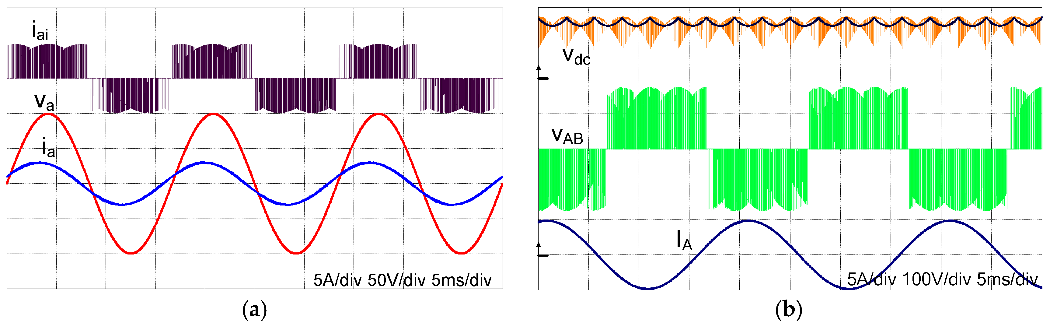
Figure 8a,b shows the input and the output side waveforms with using the conventional method when the output voltage transfer ratio, m is 0.6, and the out frequency, fout is 50 Hz. In Figure 8a, the input current of the IMC (iai) contained many switching harmonics, and its fundamental component was in phase with input voltage (va), while the input current (ia) of the power supply led the input voltage by δ = π/9. Therefore, the power factor (PF) in the input side was not at unity; the achievable power factor was 0.94.
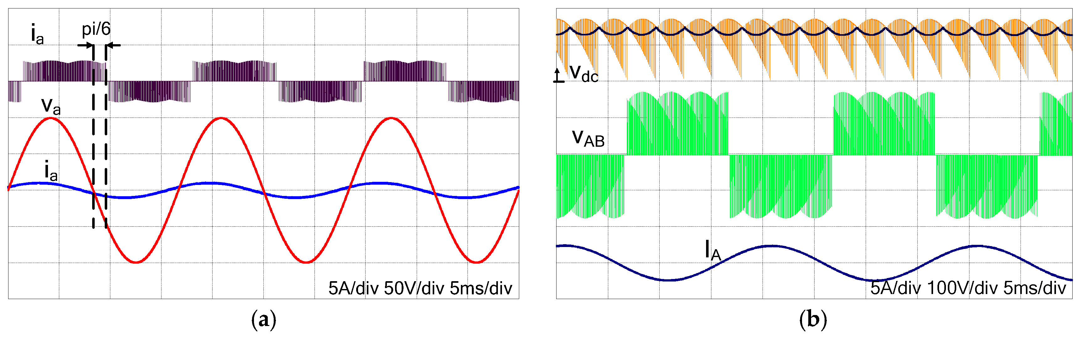
Figure 9a,b shows the input and the output side waveforms with the proposed modulation method under the same output voltage condition, with the conventional method in Figure 8. From Equation (27), the compensation angle was selected to be δcom = π/9. The input current of power supply was in phase with the input voltage, meaning that the input power factor became at unity, so that the input current magnitude became smaller under the same load condition. Contrarily, the input current of the IMC lagged behind the input voltage of power supply by π/9. Also, the output voltage/current waveforms in Figure 9b had good performance, like those in Figure 8b, although the DC-link waveform was different from that of the conventional method, due to the different modulation strategy.
In order to investigate the performance of the low output voltage operation, the output voltage references were changed to m = 0.35 and fout = 50 Hz. Figure 10 and Figure 11 show the currents and voltages at the input and output side with the conventional and the proposed methods, respectively. As mentioned before, in Figure 10a, the displacement angle between the input and output current became larger at the low output voltage δ = π/4; the input power factor was 0.71. When the proposed method was applied with the maximum compensating angle (δcom = π/6) from Figure 11, the input power factor improved to 0.91. Figure 11a shows that the IMC input current iai lagged behind the input voltage va with the desired compensated angle π/6. From Figure 11b, the proposed method provided the same output voltage performance as that in Figure 10b.
From the simulation, it was clear that the proposed method is effective in improving the input power factor without deteriorating the output performance in both cases of low and high output voltage transfer ratio.
5. Experimental Results
In order to validate the effectiveness of the proposed SVM method, a laboratory prototype was set up experimentally. Figure 12 shows the experimental setup for the IMC topology. The controller board was developed with high performance DSP (TMS320F28335, Texas Instruments, Dallas, TX, USA) and CPLD (EPM128S, Altera, San Jose, CA, USA). The power circuit of the rectifier stage was constructed by six insulated-gate bipolar transistor (IGBT) modules (SK 60GM123, Semikron, Nürnberg, Germany) and the inverter stage was composed of three dual-IGBTs (FMG2G100US60, Fairchild Semiconductor, Sunnyvale, CA, USA).
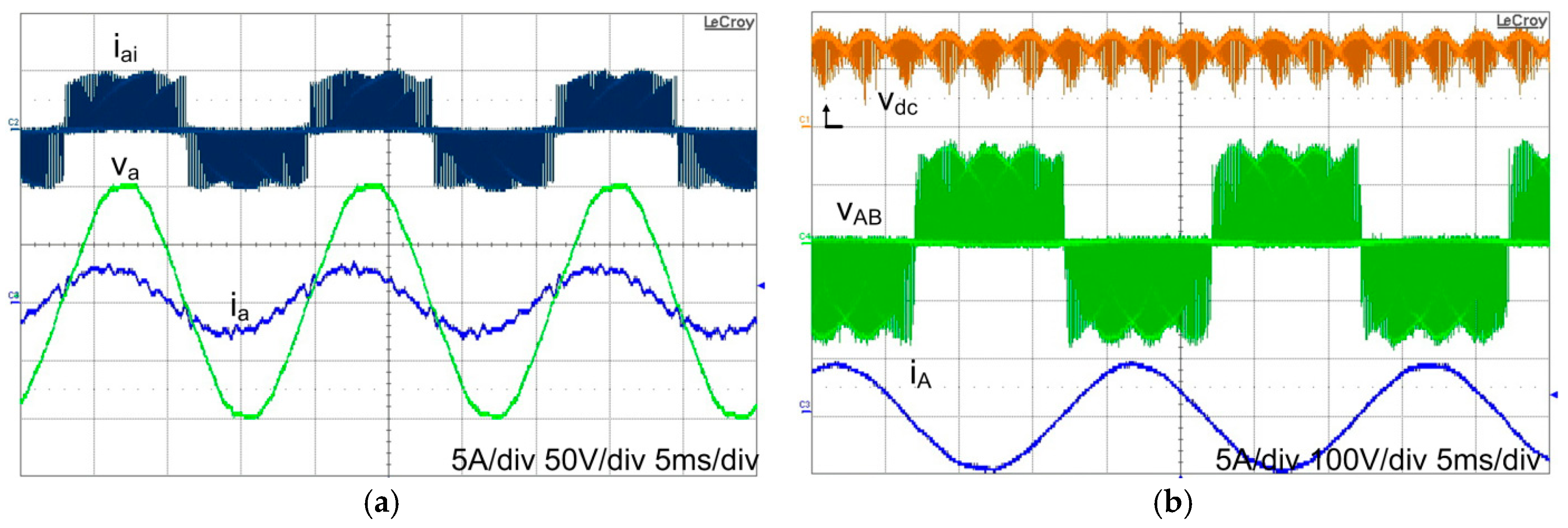
Figure 13 and Figure 14 show the input and the output waveforms with the conventional method and the proposed method, respectively, under the same load condition: m = 0.6 and fout = 50 Hz. We saw that the input power factor improved from 0.91 to unity, with the compensation angle at π/9.
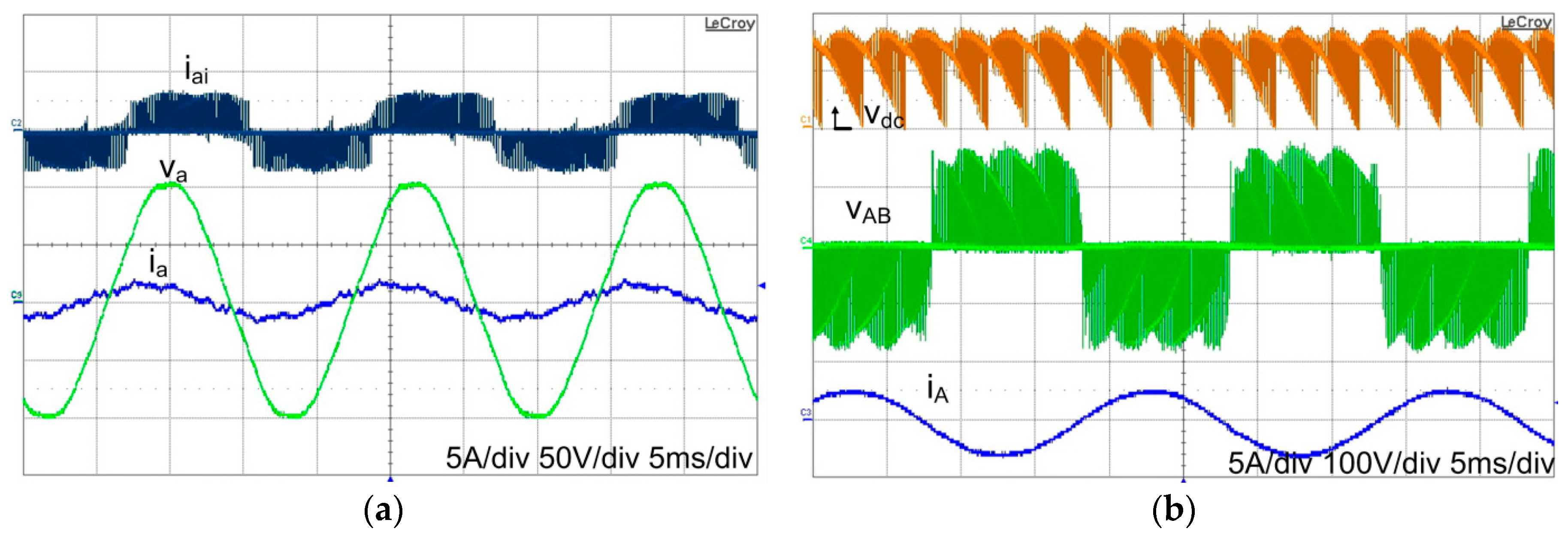
Figure 15 and Figure 16 show the experimental performance of the low voltage operation at voltage transfer ratio m = 0.35 and output frequency fout = 50Hz, with the conventional method and the proposed method, respectively. In Figure 15a, the maximum compensation angle π/6 was applied, so that the power factor improved from 0.71, which was obtained from the conventional method in Figure 15a, to 0.91. Comparing Figure 15a with Figure 16a, the input current magnitude became smaller under the proposed method, due to the improved input power factor.
As a result, the experimental results matched the simulated results very well, and the effectiveness of the proposed method was also verified by experiment as well as simulation.
6. Conclusions
This paper presents a new SVM method for the IMC to compensate for the input power factor, which is implemented by using the input voltage and the input current. Analysis, design and implementation of the proposed SVM for the three-phase IMC with the improvement of the input power factor, were presented. And also, the allowable of compensating angle according to the displacement angle caused by LC input filter is analyzed. By using the proposed SVM method, the input power factor was compensated significantly regardless of the existence of the input filter, without any performance degradation on the input/output waveforms. The unity input power factor was obtained with the proposed SVM method. Thanks to the improved power factor, the magnitude of the input current became smaller compared to the conventional method. The performance of the proposed SVM was verified with both simulation and experiment.
Acknowledgments
This research is funded by Vietnam National Foundation for Science and Technology Development (NAFOSTED) under grant number 103.99-2015.102.
Author Contributions
Phan Quoc Dzung developed the idea of this paper and performed the simulation. Nguyen Dinh Tuyen implemented the main research, performed the experiment. All authors contributed to the writing of the manuscript, revised and approved the final manuscript.
Conflicts of Interest
The authors declare no conflict of interest.
References
- Alesina, A.; Venturini, M.G.B. Solid-state power conversion: A Fourier analysis approach to generalized transformer synthesis. IEEE Trans. Circuits Syst. 1981, 28, 319–330. [Google Scholar] [CrossRef]
- Arevalo, S.L.; Zanchetta, P.; Wheeler, P.W. Control of a matrix converter-based AC power supply for aircrafts under unbalanced conditions. In Proceedings of the IECON 2007, Taipei, Taiwan, 5–8 November 2007; pp. 1823–1828. [Google Scholar]
- Sebtahmadi, S.S.; Pirasteh, H.; Kaboli, S.H.A.; Radan, A.; Mekhilef, S. A 12-sector space vector switching scheme for performance improvement of matrix-converter-based DTC of IM drive. IEEE Trans. Power Electron. 2015, 30, 3804–3817. [Google Scholar] [CrossRef]
- Jussila, M.; Eskola, M.; Tuusa, H. Analysis of non-idealities in direct and indirect matrix converters. In Proceedings of the EPE–ECCE Europe 2005, Dresden, Germany, 11–14 September 2005; pp. 1–10. [Google Scholar]
- Kolar, J.W.; Schafmeister, F.; Round, S.D.; Ertl, H. Novel three-phase AC-AC sparse matrix converters. IEEE Trans. Power Electron. 2007, 22, 1649–1661. [Google Scholar] [CrossRef]
- Nguyen, T.D.; Lee, H.H. Development of a three-to-five-phase indirect matrix converter with carrier-based PWM based on space-vector modulation analysis. IEEE Trans. Ind. Electron. 2016, 63, 13–24. [Google Scholar] [CrossRef]
- Nguyen, T.D.; Lee, H.H. Dual three-phase indirect matrix converter with carrier-based PWM method. IEEE Trans. Power Electron. 2014, 29, 569–581. [Google Scholar] [CrossRef]
- Nguyen, T.D.; Lee, H.H. Modulation strategies to reduce common-mode voltage for indirect matrix converters. IEEE Trans. Ind. Electron. 2012, 59, 129–140. [Google Scholar] [CrossRef]
- Kim, S.; Yoon, Y.D.; Sul, S.K. Pulsewidth modulation method of matrix converter for reducing output current ripple. IEEE Trans. Power Electron. 2010, 25, 2620–2629. [Google Scholar] [CrossRef]
- Nguyen, H.M.; Lee, H.H.; Chun, T.W. Input power factor compensation algorithms using a new direct-SVM method for matrix converter. IEEE Trans. Ind. Electron. 2011, 58, 232–243. [Google Scholar] [CrossRef]
Figure 1.
The indirect matrix converter (IMC) topology.
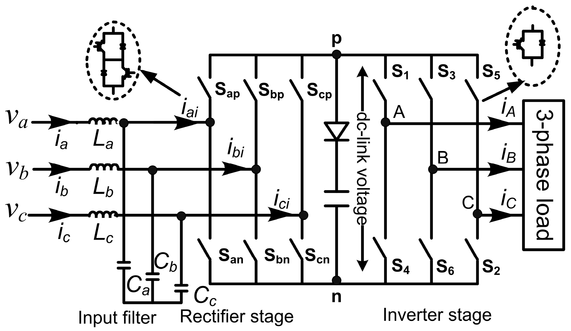
Figure 2.
The definition of input sectors.

Figure 3.
The space vector diagram of inverter stage.

Figure 4.
The switching pattern of IMC.

Figure 5.
The equivalent circuit of the input filter for phase a.
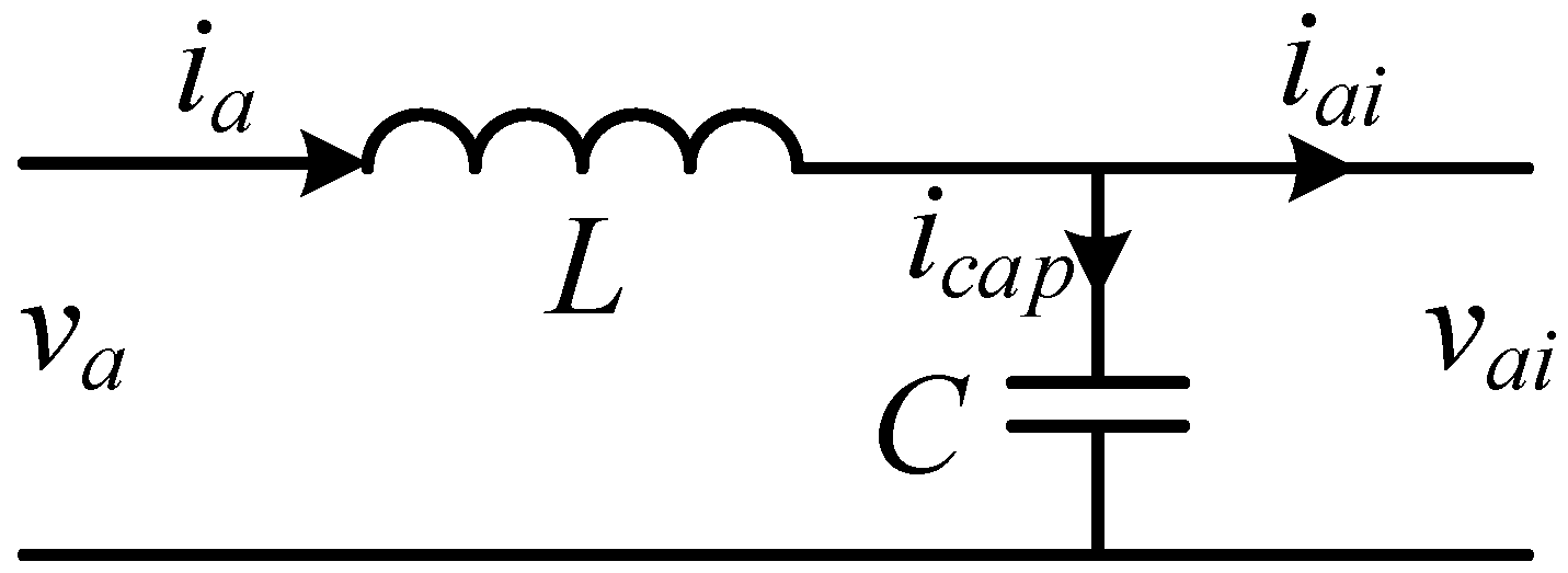
Figure 6.
The space vector diagram of rectifier stage.
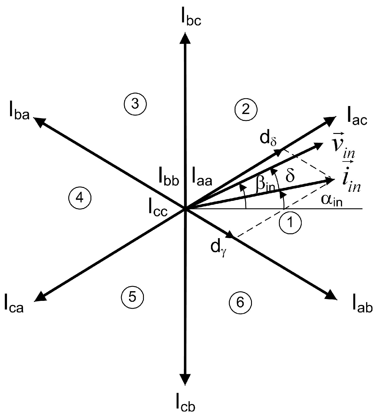
Figure 7.
The block diagram of the proposed SVM method.

Figure 8.
(a) Input waveforms; and (b) DC-link voltage and output waveforms with the conventional method at m = 0.6 and fout = 50 Hz.
Figure 8.
(a) Input waveforms; and (b) DC-link voltage and output waveforms with the conventional method at m = 0.6 and fout = 50 Hz.

Figure 9.
(a) Input waveforms; and (b) DC-link voltage and output waveforms with the proposed method at m = 0.6 and fout = 50 Hz.
Figure 9.
(a) Input waveforms; and (b) DC-link voltage and output waveforms with the proposed method at m = 0.6 and fout = 50 Hz.
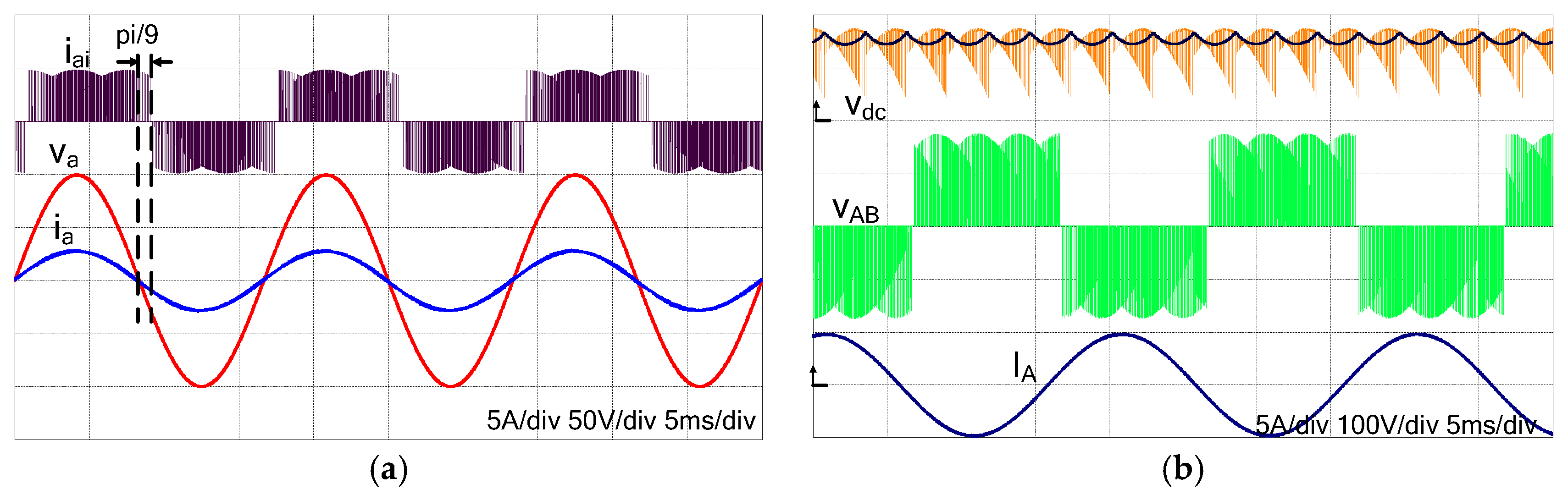
Figure 10.
(a) Input waveforms; and (b) DC-link voltage and output waveforms with the conventional method at m = 0.35 and fout = 50 Hz.
Figure 10.
(a) Input waveforms; and (b) DC-link voltage and output waveforms with the conventional method at m = 0.35 and fout = 50 Hz.
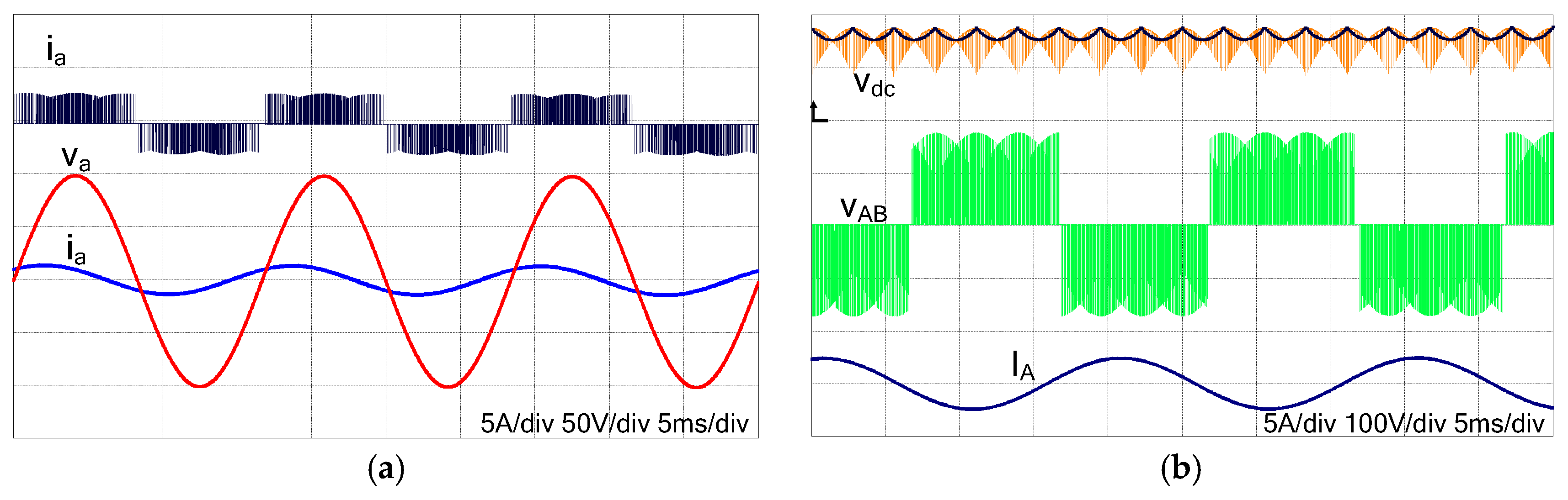
Figure 11.
(a) Input waveforms; and (b) DC-link voltage and output waveforms with the proposed method at m = 0.35 and fout = 50 Hz.
Figure 11.
(a) Input waveforms; and (b) DC-link voltage and output waveforms with the proposed method at m = 0.35 and fout = 50 Hz.

Figure 12.
Experimental setup for the IMC topology.
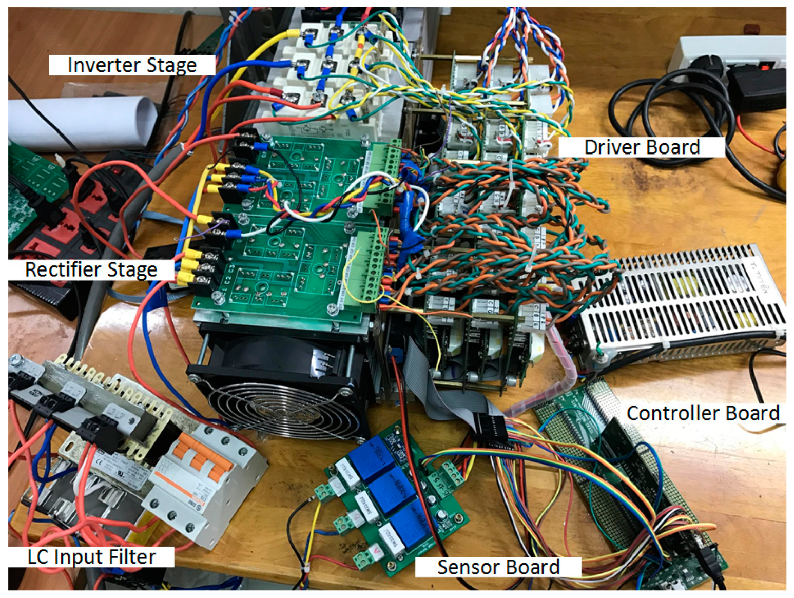
Figure 13.
(a) Input waveforms; and (b) DC-link voltage and output waveforms with the conventional method at m = 0.6 and fout = 50 Hz (PF = 0.94).
Figure 13.
(a) Input waveforms; and (b) DC-link voltage and output waveforms with the conventional method at m = 0.6 and fout = 50 Hz (PF = 0.94).

Figure 14.
(a) Input waveforms; and (b) DC-link voltage and output waveforms with the proposed method at m = 0.6 and fout = 50 Hz (PF = 1.0).
Figure 14.
(a) Input waveforms; and (b) DC-link voltage and output waveforms with the proposed method at m = 0.6 and fout = 50 Hz (PF = 1.0).
Figure 15.
(a) Input waveforms; and (b) DC-link voltage and output waveforms with the conventional method at m = 0.35 and fout = 50 Hz (PF = 0.71).
Figure 15.
(a) Input waveforms; and (b) DC-link voltage and output waveforms with the conventional method at m = 0.35 and fout = 50 Hz (PF = 0.71).
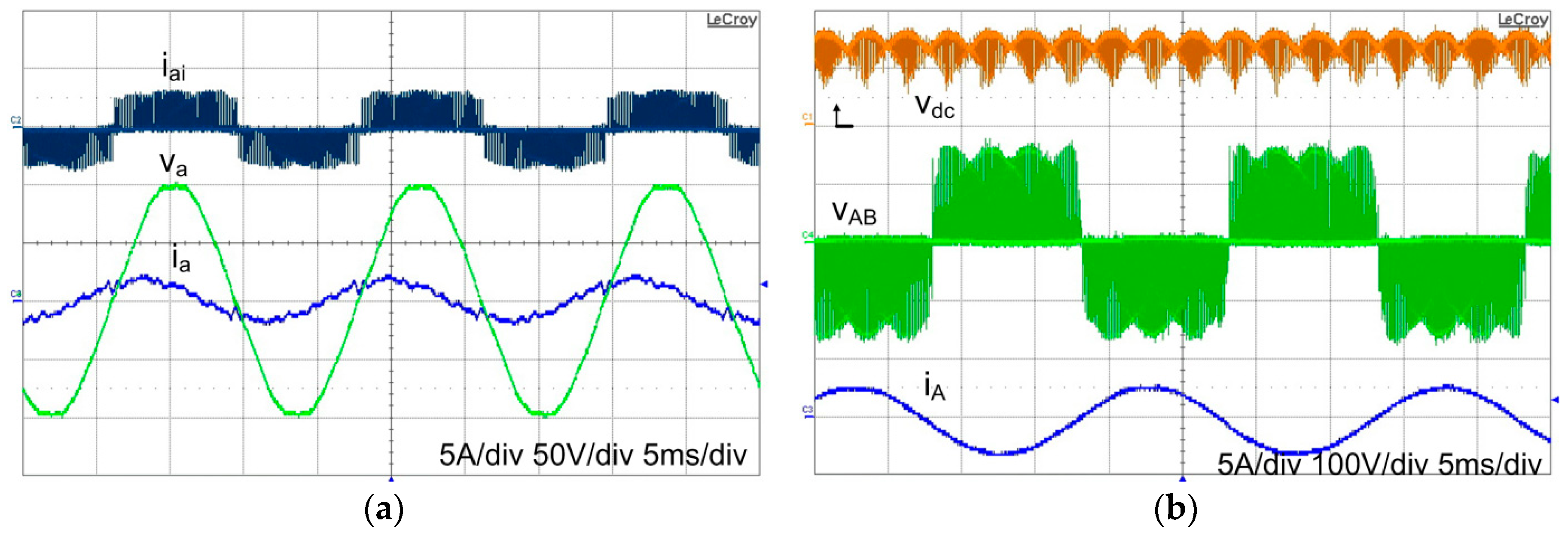
Figure 16.
(a) Input waveforms; and (b) DC-link voltage and output waveforms with the proposed method at m = 0.35 and fout = 50 Hz (PF = 0.91).
Figure 16.
(a) Input waveforms; and (b) DC-link voltage and output waveforms with the proposed method at m = 0.35 and fout = 50 Hz (PF = 0.91).


Table 1.
The switching states and their DC-link voltages according to the input sector.
| Input Sector | Conducting Switch | Modulated Switches | Dc-Link Voltage | Average Value (Vdc) |
|---|---|---|---|---|
| 1 | Sap | Sbn, Scn | vab, vac | |
| 2 | Scn | Sap, Sbp | vac, vbc | |
| 3 | Sbp | San, Scn | vba, vbc | |
| 4 | San | Sbp, Scp | vba, vca | |
| 5 | Scp | Sbn, San | vcb, vca | |
| 6 | Sbn | Sap, Scp | vab, vcb |
Table 2.
The input current space vectors according to the switching State.
| Switching State | Input Current | ||||||
|---|---|---|---|---|---|---|---|
| Sap | Sbp | Scp | San | Sbn | Scn | Iin | αin |
| 1 | 0 | 0 | 0 | 1 | 0 | ||
| 1 | 0 | 0 | 0 | 0 | 1 | ||
| 0 | 1 | 0 | 0 | 0 | 1 | ||
| 0 | 1 | 0 | 1 | 0 | 0 | ||
| 0 | 0 | 1 | 1 | 0 | 0 | ||
| 0 | 0 | 1 | 0 | 1 | 0 | ||
| 1 | 0 | 0 | 1 | 0 | 0 | 0 | x |
| 0 | 1 | 0 | 0 | 1 | 0 | 0 | x |
| 0 | 0 | 1 | 0 | 0 | 1 | 0 | x |
© 2017 by the authors. Licensee MDPI, Basel, Switzerland. This article is an open access article distributed under the terms and conditions of the Creative Commons Attribution (CC BY) license (http://creativecommons.org/licenses/by/4.0/).
Share and Cite
MDPI and ACS Style
Tuyen, N.D.; Dzung, P.Q. Space Vector Modulation for an Indirect Matrix Converter with Improved Input Power Factor. Energies 2017, 10, 588. https://doi.org/10.3390/en10050588
AMA Style
Tuyen ND, Dzung PQ. Space Vector Modulation for an Indirect Matrix Converter with Improved Input Power Factor. Energies. 2017; 10(5):588. https://doi.org/10.3390/en10050588
Chicago/Turabian StyleTuyen, Nguyen Dinh, and Phan Quoc Dzung. 2017. "Space Vector Modulation for an Indirect Matrix Converter with Improved Input Power Factor" Energies 10, no. 5: 588. https://doi.org/10.3390/en10050588
Note that from the first issue of 2016, this journal uses article numbers instead of page numbers. See further details here.