1. Introduction
In the past few years, perovskite solar cells (PSCs) have received a considerable amount of attention because of their notable advantages, including solution fabrication processes, large absorption coefficients, long exciton diffusion lengths, and high power conversion efficiency (PCE) values [
1,
2,
3]. At present, PSC structures can be mainly divided into two species: conventional structures, which originated from the concept of dye-sensitized solar cells [
4,
5,
6,
7], and inverted structures, which originated from the concept of organic solar cells (OSCs) [
8,
9,
10,
11,
12,
13,
14]. Conventional structures are composed of a transparent conductive oxide (TCO) substrate/electron transport layer (ETL)/perovskite layer/hole transport layer (HTL)/anode, whereas inverted structures are composed of a TCO substrate/HTL/perovskite layer/ETL/cathode. The TCO substrates used in the conventional and inverted structures are Fluorine doped tin oxide (FTO) and indium tin oxide (ITO), respectively, which are attributed to the fabrication process in temperature treatment. The ETL materials used in the conventional structures are usually Titanium oxide (TiO
2), Aluminum oxide (Al
2O
3), and Zinc oxide (ZnO) [
7,
15], and the HTL materials used in the conventional structures are poly(triarylamine) (PTAA) and 2,2′,7,7′-tetrakis-(N,N-di-
p-methoxy-phenylamine)-9,9′-bifluorene (Spiro-OMeTAD) [
15,
16]. On the other hand, the HTL and ETL materials for the inverted structures are poly(3,4-ethylenedioxythiophene): poly(styrenesulfonate) (PEDOT:PSS) and [6,6]-phenyl C
61-butyric acid methyl ester (PCBM), respectively [
8,
9,
10,
11]. In general, the performance of PSCs mainly relies on the quality of the perovskite film, particularly in the inverted structure, which does not have a mesoscopic structure to control crystal growth in the film. The solution engineering process has two methods to achieve PSCs: one-step coating and two-step coating. One-step coating involves directly spin-coating a synthetic solution with solvent on the patterned substrate. Two-step coating is another deposition process in which the patterned substrate would be immersed into a solution to fabricate the perovskite thin film after spin-coating the perovskite precursor onto a patterned substrate. The difference between the two fabrication methods is the quality of the resulting perovskite thin film, which is controlled by the optimized crystallization for two-step coating and low-cost with simple fabrication for one-step coating. Therefore, solution engineering of high-quality perovskite films was proposed and investigated by many groups [
11,
16,
17,
18]. The efficiency of conventional structure not only depends on the solvent, but also on the TiO
2 meso-structure. The growth of TiO
2 thin films is beneficial to the growth of perovskite films. In other words, the quality of the perovskite film can be controlled via the TiO
2 structure. This is different from the inverted structure which is mainly controlled by the addition of solvent. This is attributed to the fact that the inverted structure perovskite film is coated on the smooth PEDOT:PSS layer. As a result, the solvents used in the inverted structure have more influence on the PCE of the resulting device compared to the conventional structure case.
In this section, perovskite layers of methylammonium lead halide (CH
3NH
3PbI
3) fabricated using various solvents are investigated. The efficiency of the devices in this study is lower than that of devices reported in the literature [
10,
11,
16,
17,
18] because of the inverted structure and the usage of fullerene (C
60). However, the thickness of C
60 can be precisely controlled at 30 nm via thermal evaporation to obtain stable device parameters, which can accurately reveal the effect of different solvents in PSC fabrication. This observation shows that the characteristics of perovskite layers from various solvents are differences in absorption, surface roughness, film coverage, and crystallization, all of which lead to the variation of efficiency n in PSCs. The quality of perovskite layers is also significantly associated with the properties of the solvents. A detailed investigation of the relation between the PCE and the solvents is presented. As a result, an optimized solvent for the fabrication of perovskite layer is proposed to further improve the PCE of PSCs.
2. Results and Discussion
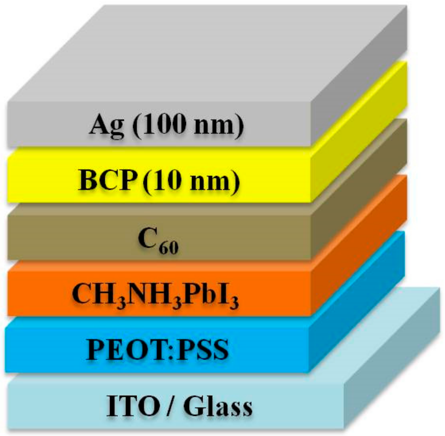
The device structure is shown in
Figure 1.
Figure 2 shows the
J–V characteristics of the PSCs fabricated using various solvents (i.e., γ-butyrolactone (GBL), dimethyl sulfoxide (DMSO), DMSO: dimethylformamide (DMF), and DMSO:GBL). The performance parameters of the devices are listed in
Table 1.
The device fabricated using DMF as solvent showed a PCE of 0 (not shown in
Figure 2) because the current density–voltage (
J–V) curve passed through the origin. The PCEs of the devices fabricated using GBL and DMSO were 1.74% and 8.37%, whereas the PCEs of the device using the mixed solvents DMSO:DMF and DMSO:GBL were 7.64% and 9.77%. The results showed that the performance of the PSCs was significantly influenced by the CH
3NH
3PbI
3 layer fabricated with different solvents.
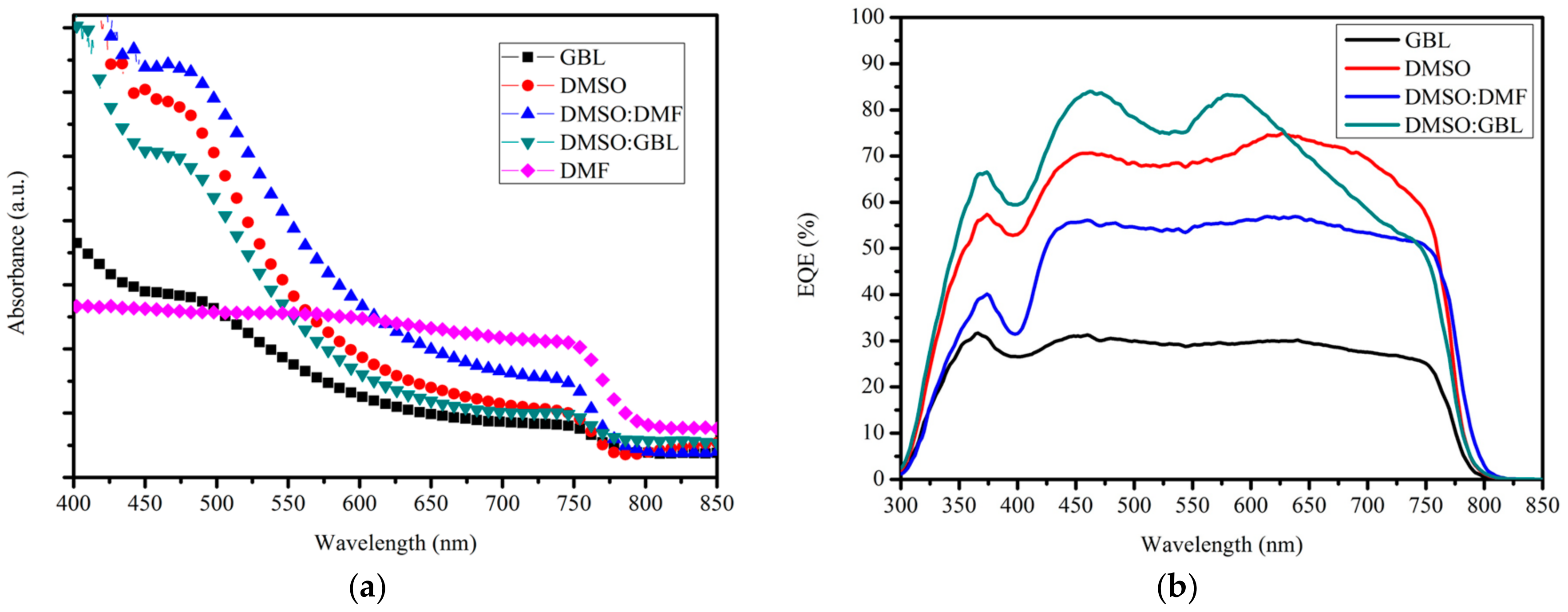
Figure 3a,b shows the absorption spectra of the perovskite layers and external quantum efficiency (EQE) spectra of the devices fabricated using various solvents. The low absorption of the CH
3NH
3PbI
3 layer fabricated from DMF was attributed to the discontinuous film coverage on the ITO/PEDOT:PSS substrate and the low crystallization content in the film. The low absorption of the CH
3NH
3PbI
3 layer fabricated from GBL was ascribed to the low solubility in this solvent of the materials PbI
2 and CH
3NH
3I. This observation is discussed in the next section. The absorption coefficients of the CH
3NH
3PbI
3 layers fabricated from the solvents containing DMSO were higher than that of CH
3NH
3PbI
3 layers fabricated from DMF or GBL because of the large amount of crystallization in the film and uniform film coverage (as shown in the next section).
High absorption was achieved in the perovskite layer fabricated from DMSO:DMF solvent. However, the best device efficiency corresponded to the one fabricated from DMSO:GBL rather than from DMSO:DMF. The trend of the EQE spectra was different from that of the absorption spectra. This outcome indicated that the light transformation for the electron did not depend only on the absorption efficiency. The EQE can be interpreted as follows [
19]:
where
ηA is the absorption efficiency of incident photons,
ηED is the efficiency of photogenerated excitons that diffuse to the heterojunction interface,
ηCT is the charge transfer efficiency, and
ηCC is the charge collection efficiency. In this case, the EQE spectra of the devices were associated with the
ηA and
ηCC. The
ηCC could be explained and analyzed based on the quality of the perovskite layers fabricated using different solvents.
Figure 4 shows the microscope images and surface morphologies of the CH
3NH
3PbI
3 layers fabricated using various solvents. The surface image and morphology of the CH
3NH
3PbI
3 layer fabricated using DMF as solvent showed poor coverage on the ITO/PEDOT:PSS substrate, and the root mean square roughness (
Rq) of the layer was as high as 279 nm. This result was attributed to the low adhesion and high evaporation rate of DMF [
17]; thus, the film could not be uniformly sprayed on the substrate. This scenario leads to a shunting path between the ITO and Ag, and the
J–V curve passed through the origin. In GBL, the surface image exhibited many large black points assigned to the materials PbI
2 or CH
3NH
3I, and the
Rq of the film was 102 nm. This result was attributed to the low solubility and weak coordination of GBL towards PbI
2 and CH
3NH
3I, thereby resulting in the separation of the material out of the solvent during the spin coating. Thus, compared with other devices, the device using GBL as solvent had high series resistance (
Rs, 53.9 Ω × cm
2) and low shunt resistance (
Rsh, 163 Ω × cm
2). By contrast, the surface image of perovskite layer produced in DMSO solvent showed full coverage without apparent defects on the substrate, and the
Rq of film was 14.17 nm. These results were ascribed to the strong coordination and the large solubility of PbI
2 and CH
3NH
3I and of DMSO. The smooth surface could effectively depress the leakage current and increase the
Rsh of the device, thus improving the fill factor (
FF) from 0.36 to 0.72 and the PCE from 1.74% to 8.37% by substituting DMSO for GBL. However, the surface image of the perovskite layer fabricated with the addition of DMF into DMSO was apparently changed. The surface morphology showed cracks everywhere, and the
Rq of the film was up to 34.37 nm. The result could be a result of the high evaporation rate of DMF, leading to the fast formation of crystalline CH
3NH
3PbI
3 on the surface, a decrease of the
Rsh from 684 Ω × cm
2 to 484 Ω × cm
2, and a decrease of the
FF from 0.72 to 0.63 using DMSO:DMF. The
Rq of the perovskite layer fabricated from DMSO:GBL was only 6.01 nm. The roughness of the perovskite layer made from DMSO:GBL was less than that of the perovskite layer prepared from pure DMSO. The
Rsh and
FF of the device fabricated using DMSO:GBL increased to 1021 Ω × cm
2 and 0.77, respectively.
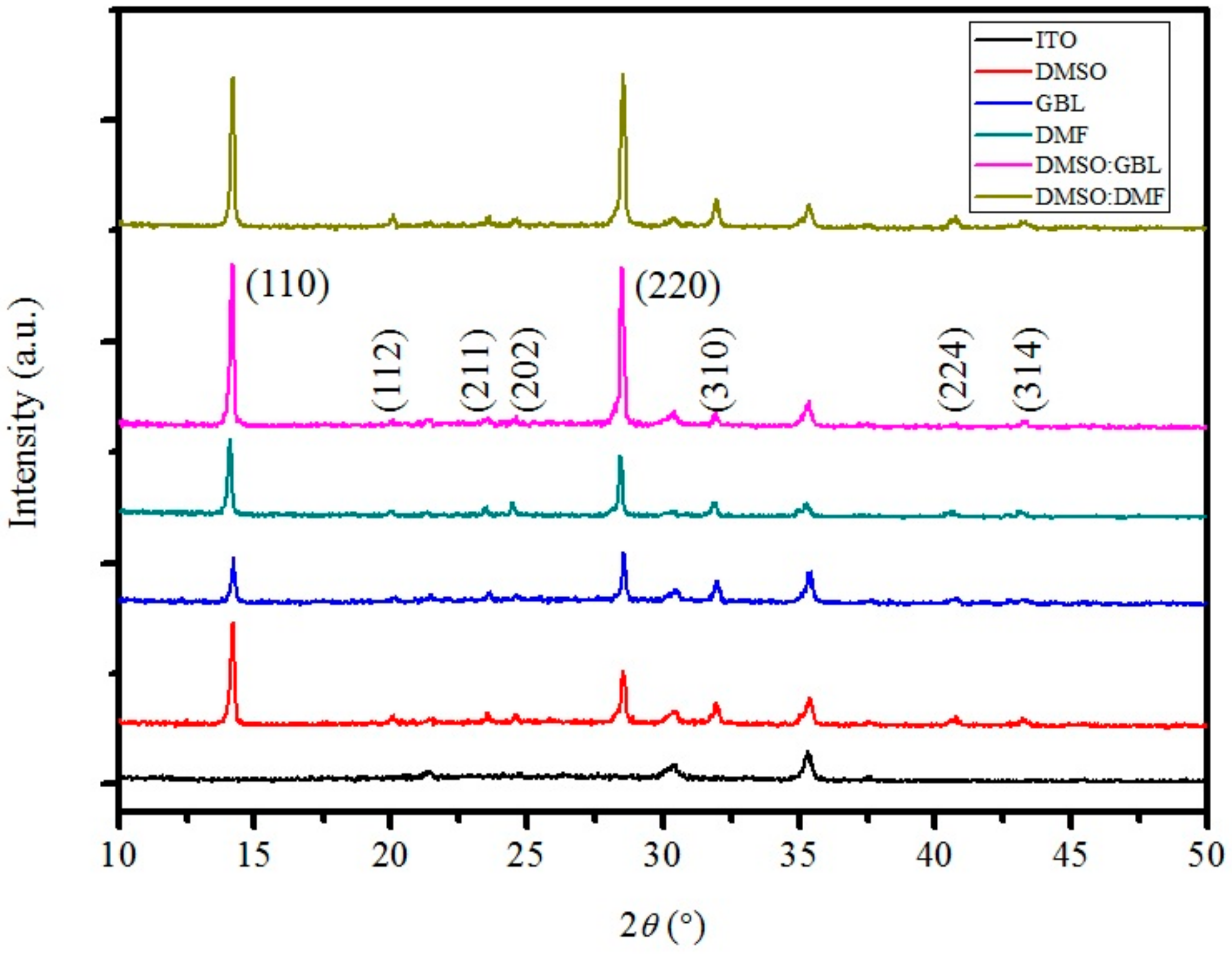
Figure 5 shows the X-ray diffraction (XRD) patterns of the ITO and CH
3NH
3PbI
3 layers fabricated using various solvents. The peaks of the perovskite layer at 14.2°, 21.46°, 23.56°, 24.58°, 28.54°, 31.98°, 40.78°, and 43.24° correspond to the (110), (112), (211), (202), (220), (310), (224), and (314) planes, respectively [
5,
6,
15]. This finding shows that the perovskite layers produced from the different solvents are highly crystalline structures without other PbI
2 and CH
3NH
3I peaks being observed. The XRD patterns of the perovskite layers from different solvents are approximately the same, except for the intensity at the (110) and (220) planes. This finding indicates that the amounts of crystalline material at the (110) and (220) planes are different. The XRD patterns of the perovskite layers made from DMF and GBL reveal the low crystalline content in the films, consistent with the absorption spectra and the surface images.
The XRD patterns of the perovskite layers fabricated from mixed solvents show a large amount of crystalline material at the (110) and (220) planes. This result is ascribed to the strong coordination of DMSO, forming the MAI-PbI
2-DMSO complex, which can retard the rate of crystallization of perovskite structures [
16,
18] and lead to high quality films (as shown in
Figure 4). However, the XRD pattern of the perovskite layer from pure DMSO shows a relatively lower intensity than that prepared from the mixed solvent. This low intensity results from the low evaporation rate of the DMSO, a rate that complicates the arrangement of crystals. Therefore, the highest PCE is obtained from the perovskite layer fabricated using DMSO:GBL because of the smooth surface, full coverage on the substrate, and high film crystallization. The open-circuit voltage (
Voc) values of the devices fabricated using different solvents are approximately the same, except for the
Voc of the device using the mixed DMSO:DMF solvent. This finding needs further investigation of the effect on the
Voc variation of PSCs.
Finally, the mixed solvent DMSO:DMF:GBL at a volume ratio of 5:2:3, which combines the advantages of each solvent, was used to fabricate the perovskite layer. As a result, the PCE of the device is further improved to 10.84% with a short current density (Jsc) of 18.02 mA/cm2, a Voc of 0.77 V, and an FF of 0.78. The intrinsic vulnerability of PSCs to ambient moisture and water remains an open and important problem. It is interesting that the device made using DMSO as solvent is more stable than the device made with DMF or GBL solvents due to the better quality of the perovskite film. The PCE of that device is almost the same after 24 h. However, the device with GBL solvent only has the half of PCE. The devices with only DMF solvent are unstable due to the atrociously thin films formed, causing that the PCE of the device to be very low and mostly fail due to the shunting path. In other words, the choice of solvent can directly affect the stability of PSCs. Further improvement of inherent stability is expected by growing a water-resistive coating on or ion doping into perovskite films in the future.
3. Materials and Methods
The ITO–glass substrates (AimCore Technology, Hsinchu, Taiwan) with a sheet resistance of 7 Ω/sq were sequentially cleaned by performing ultrasonic treatment in acetone, methanol, and deionized water for 5 min each, and then dried under a nitrogen blow. The oxygen (O
2) plasma treatment on the ITO substrate was conducted using radio frequency (RF) power at 10 W for 2 min at the pressure of 0.45 torr. The PEDOT:PSS layer was spin coated on the precleaned ITO at 5000 rpm for 30 s and baked at 120 °C for 15 min. Then, 0.198 g CH
3NH
3I (>98%, Dyesol, Queanbeyan, Australia) and 0.576 g PbI
2 (99.99%, Alfa Aesar, Haverhill, MA, USA) were dissolved and stirred at 50 °C for 12 h in 1 mL various solutions of DMF, GBL, DMSO, a mixture of DMSO and DMF (DMSO:DMF, 1:1
v/
v), and a mixture of DMSO and GBL (DMSO:GBL, 1:1
v/
v) to prepare the CH
3NH
3PbI
3 precursor solutions. The CH
3NH
3PbI
3 precursor solution was spin coated on the PEDOT:PSS layer to form a perovskite layer [
18]. The materials of C
60 and BCP were used as an electron acceptor and an ETL, respectively. The organic materials and Ag were deposited via vacuum thermal evaporation under a pressure of 4.8 × 10
−6 torr. The deposition rate of the organic materials was approximately 0.02–0.04 nm/s, and Ag was deposited through a shadow mask, yielding an active area of 0.2 cm
2 at a deposition rate of 0.1 nm/s. The deposition rate and film thickness were monitored using a quartz crystal oscillator.
The J–V characteristics of PSCs were measured using a power source meter (Keithley 2400, Keithley, Cleveland, AL, USA) under an illumination of 100 mW/cm2 produced by an AM1.5G sun simulator (Oriel 96,000 150 W Xe lamp, Newport, Taipei, Taiwan). The light intensity was calibrated using a reference solar cell and meter (Oriel 91150, Newport). All the devices were encapsulated, and the active area was masked with a metal mask (area of 6 mm2) before the measurement of J–V characteristics was executed to ensure the reliability and accuracy of parameters. For atomic force microscope (AFM) measurement (XE-70, Park Systems, Suwon, Korea), the surface morphologies were determined in noncontact mode in air. The absorption spectra of the films were measured using a UV–vis–NIR spectrophotometer (UV-3900, Hitachi, Tokyo, Japan) in the 400–850 nm wavelength range. The EQE measurements were performed using Solar Cell QE/IPCE measurement system (QE-3000, Titan Electro-Optics, Taipei, Taiwan). The EQE spectra were performed with a SR830 lock-in amplifier (Stanford Research System, Titan Electro-Optics, Taipei, Taiwan) under monochromatic illumination at a chopping frequency of 185 Hz. The XRD data were measured by a Rigaku/Ultima IV X-ray diffractometer (Tokyo, Japan).


