
A High-Power-Density Single-Phase Rectifier Based on Three-Level Neutral-Point Clamped Circuits

1
School of Electrical Engineering, Southwest Jiaotong University, Chengdu 610031, China
2
State Grid Suining Power Supply Company, Suining 629000, China
3
Monolithic Power Systems, Shenzhen 518000, China
*
Author to whom correspondence should be addressed.
Energies 2017, 10(5), 697; https://doi.org/10.3390/en10050697
Submission received: 19 March 2017
/
Revised: 5 May 2017
/
Accepted: 9 May 2017
/
Published: 16 May 2017
(This article belongs to the Special Issue Power Electronics in Power Quality)
Abstract
:A single-phase three-level converter is suitable for medium-power applications, with an interface voltage that is higher than that of a traditional two-level configuration. The three-level neutral-point clamped converter is adopted using four switches in each bridge arm, which, compared to a two-level rectifier, leads to less voltage stress, a lower switching frequency, and switching loss on switches. The transient current control strategy is designed to control the active power. The single-phase space vector pulse width modulation (SVPWM) with a voltage balance strategy is designed to solve the neutral point voltage fluctuation problem and keep the dc-link voltage stable. A 1.3 kW high-power-density prototype based on SiC MOSFET was built and tested. The experimental results verified the high performance of steady-state and dynamic responses.
1. Introduction
Due to the existence of non-linear loads such as uncontrolled rectifiers, the significant harmonics and reactive power will be generated and flow into the grid, which will reduce the grid power quality, influence power distribution, cause incorrect operation, and even damage electric apparatuses. A controlled rectifier can control the dc-link voltage stable at a constant value, and lower harmonics and lower total harmonic distortion (THD) exists on the grid side. A power electronic converter requires a high power density and a low harmonic. Several main topologies are found and designed in the industrial acceptance, and various multilevel converter topologies, including the three-level neutral point clamped converter (3L-NPC), modular multilevel converter, and cascaded H-bridge, are widely used in power applications [1,2].
The modulation of the converter becomes complicated when the output voltage of the converter increases [3,4]. However, the fluctuation of neutral point voltage in the 3L-NPC exists if no voltage balancing measures are taken. To solve the fluctuation, auxiliary circuits for balancing the multilevel converter neutral point voltage have been proposed in [5,6,7]. Auxiliary circuits can achieve a voltage balance, but additional hardware costs also arise. The authors of [8], to cancel the auxiliary circuits, used a balance strategy adjusting the duty time of the redundant vector to solve the fluctuation problem. Peng et al. [9] proposed a smooth switching technique to solve the fluctuation.
Along with the development of semiconductor technology, new Wide Band Gap (WBG) semiconductor devices such as SiC devices have gradually come into view [10,11,12,13,14]. SiC devices enjoy a higher bandgap energy, a higher critical electric field, a higher saturation velocity, and superior thermal conductivity directly in comparison with Si devices, which means SiC devices have lower switching loss and no reverse recovery. Moreover, the great heat dissipation ability of SiC devices can withstand high voltages and high temperatures [15]. Thus, the volume of the power device can be greatly reduced and the efficiency of the system can be greatly improved.
In the traditional traction power supply system, the grid voltage needs to step down from the traction transformer first, and the AC voltage can then be rectified. In the cascade power electronic transformer, the grid voltage is applied directly to the cascade rectifier. The voltage stress of each switching device in two-level topology is larger than that in the three-level topology; it is necessary to adapt a three-level topology to efficaciously decrease voltage stress. Furthermore, SiC devices can withstand high voltage, so SiC MOSFETs are applied in the single-phase three-level topology, and the combination of SiC devices and three-level topology can effectively reduce the number of cascade rectifiers.
According to characteristics of the 3L-NPC and SiC devices, a high-power-density single-phase three-level PWM rectifier based on a SiC MOSFET prototype was designed. This system might work in the unity power factor with relatively high efficiency. This paper introduces the circuit configuration and the control algorithm of the three-level singe-phase rectifier. The performances of the designed rectifier were verified with simulations and experiments.
2. Configuration
The circuit configuration of the single-phase 3L-NPC rectifier is illustrated in Figure 1. It is composed of an input inductance , SiC MOSFET with an anti-parallel diode, clamped diodes, a second-order harmonic filter module, and loads, and the two legs are defined as and . and represent the voltage of dc-link capacitors, C1 and C2, respectively. As is well known, each 3L-NPC arm can output three-level voltage, then the terminal voltage of an H-bridge circuits can output five-level waveform as shown in Figure 1b. The terminal voltage is divided into four sections: Section I: ; Section II: ; Section III: ; Section IV: .
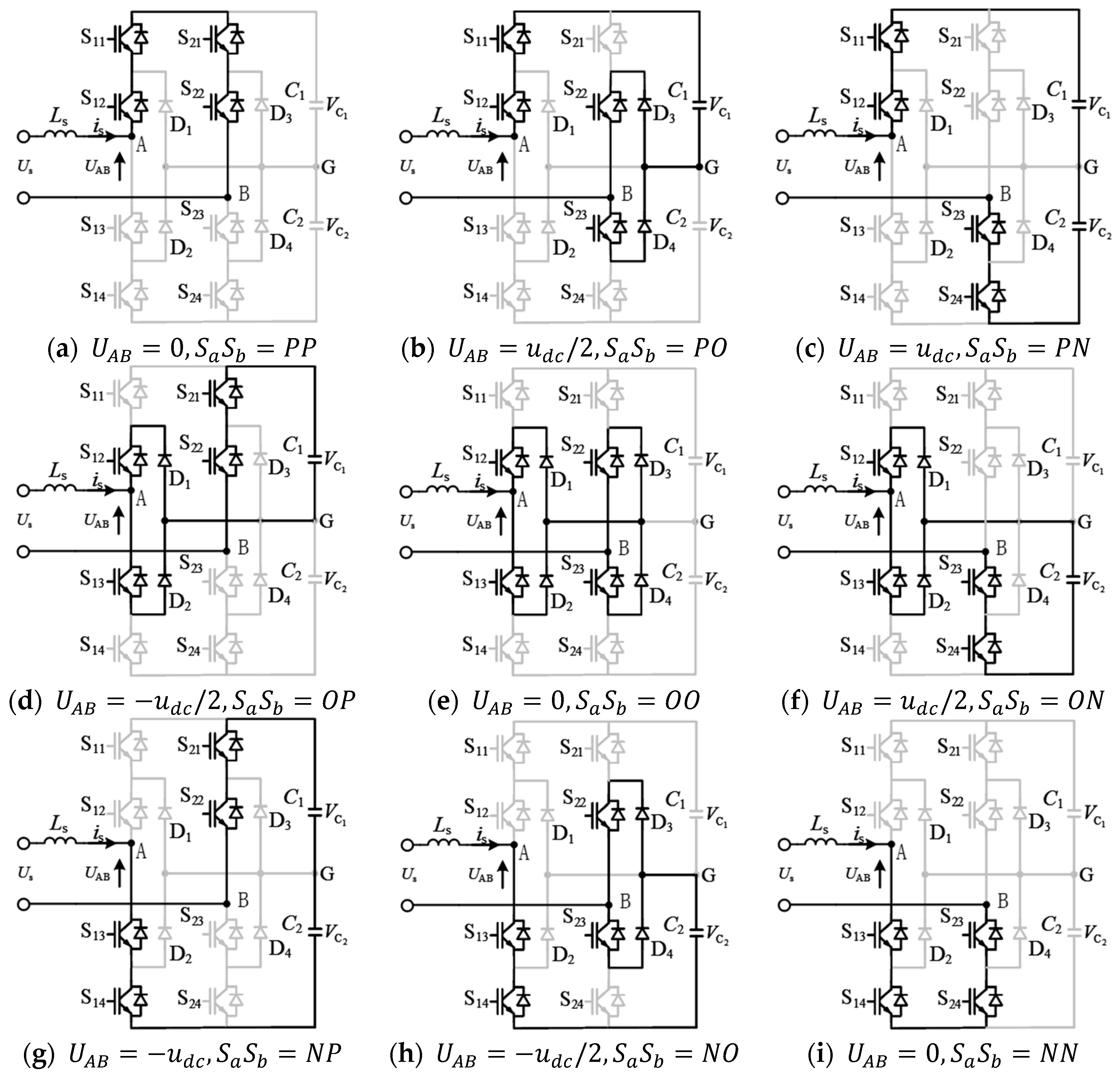
According to the circuit operation of Figure 1a, the 3L-NPC converter has nine switching states as illustrated in Figure 2a–i. Assuming that the voltage balance strategy operates properly, the details of each state are summarized as follows.
- (a)
- State 1: Switches S11, S12, S21, and S22 are on, while the others are off. The input voltage UAB is zero, and input has no effect on C1 or C2. When is > 0, the current passes through the parallel diode of S11 and S12 first, and then passes through the S21 and S22. When is < 0, the current passes through the parallel diode of S21 and S22 first, and then passes through the S11 and S12.
- (b)
- State 2: Switches S11, S12, S22, and S23 are on, while the others are off. The input voltage UAB is VC1, and C1 is charged when is > 0 and discharged when is < 0, while input has no effect on C2.
- (c)
- State 3: Switches S11, S12, S23, and S24 are on, while the others are off. The input voltage UAB is VC1 + VC2, and C1 and C2 are charged when is > 0 and discharged when is < 0.
- (d)
- State 4: Switches S12, S13, S21, and S22 are on, while the others are off. The input voltage UAB is −VC1, and C1 is discharged when is > 0 and charged when is < 0, while input has no effect on C2.
- (e)
- State 5: Switches S12, S13, S22, and S23 are on, while the others are off. The input voltage UAB is zero, and input has no effect on C1 or C2.
- (f)
- State 6: Switches S12, S13, S23, and S24 are on, while the others are off. The input voltage UAB is VC2, and C2 is charged when is > 0 and discharged when is < 0, while input has no effect on C1.
- (g)
- State 7: Switches S13, S14, S21, and S22 are on, while the others are off. The input voltage UAB is −VC1-VC2, and C1 and C2 are discharged when is > 0 and charged when is < 0.
- (h)
- State 8: Switches S13, S14, S22, and S23 are on, while the others are off. The input voltage UAB is −VC2, and C2 is discharged when is > 0 and charged when is < 0, while input has no effect on C1.
- (i)
- State 9: Switches S13, S14, S23, and S24 are on, while the others are off. The input voltage UAB is zero, and input has no effect on C1 or C2.
The definition of P is that the two switches of the bridge arm Si (i = 1, 2)—Si1 and Si2—are on, the definition of O is that Si2 and Si3 are on, and the definition of N is that Si3 and Si4 are on.
The effect of each state on the two capacitor voltages was analyzed based on nine switching states, and the situation where the grid current is taken as an example, as shown in Table 1. State PO charges Capacitor C1 only while State PO has no effect on Capacitor C2, State OP discharges Capacitor C1 only while State OP has no effect on Capacitor C2, State ON charges Capacitor C2 only while State ON has no effect on Capacitor C1, and State NO charges Capacitor C2 only while State NO has no effect on Capacitor C1. All four of these switching states cause fluctuation of the neutral point voltage. The solution of the fluctuation is discussed in the next section.
3. Control Algorithm and Modulation
The configuration of the control system is shown in Figure 3a. The transient current control strategy utilizes the grid current , the input voltage , the dc-link voltage , and the dc-link current to generate the modulation signal . The redundant vector select strategy and SVPWM methods use and the voltages of two capacitors to generate switch signals.
3.1. Transient Current Control Strategy
The transient current control diagram is shown in Figure 3b, where and are the reference and actual value of the dc-link voltage, and is the gain constant. The phase-locked loop (PLL) is a phase lock procedure, which detects the phase of input voltage.
The voltage control part utilizes a standard PI (Proportional Integral) controller to maintain the dc-link voltage, which should be stable and equal to the reference. When , the input current will increase and input power will raise, as shown in Equation (1), so the change in power required is shown by the output of the PI controller, that is, the given value of Is.
In order to improve the dynamic characteristics of the PI controller, load current feed-forward control is adopted as in Equation (2), the effective component of a given current is calculated by the input voltage, the dc-link voltage, and the current. The amplitude of the grid current consists of a feed-forward controller output of Equation (2) and the PI controller output of Equation (1), where the feed-forward output is
Then, the instantons current reference is accumulated as
The current control part has a fast response ability. As shown in Equation (4), and compose the , guarantees that the actual current tracks the reference current in real-time, and the output is the instruction value of modulation signal .
3.2. Space Vector Pulse Width Modulation
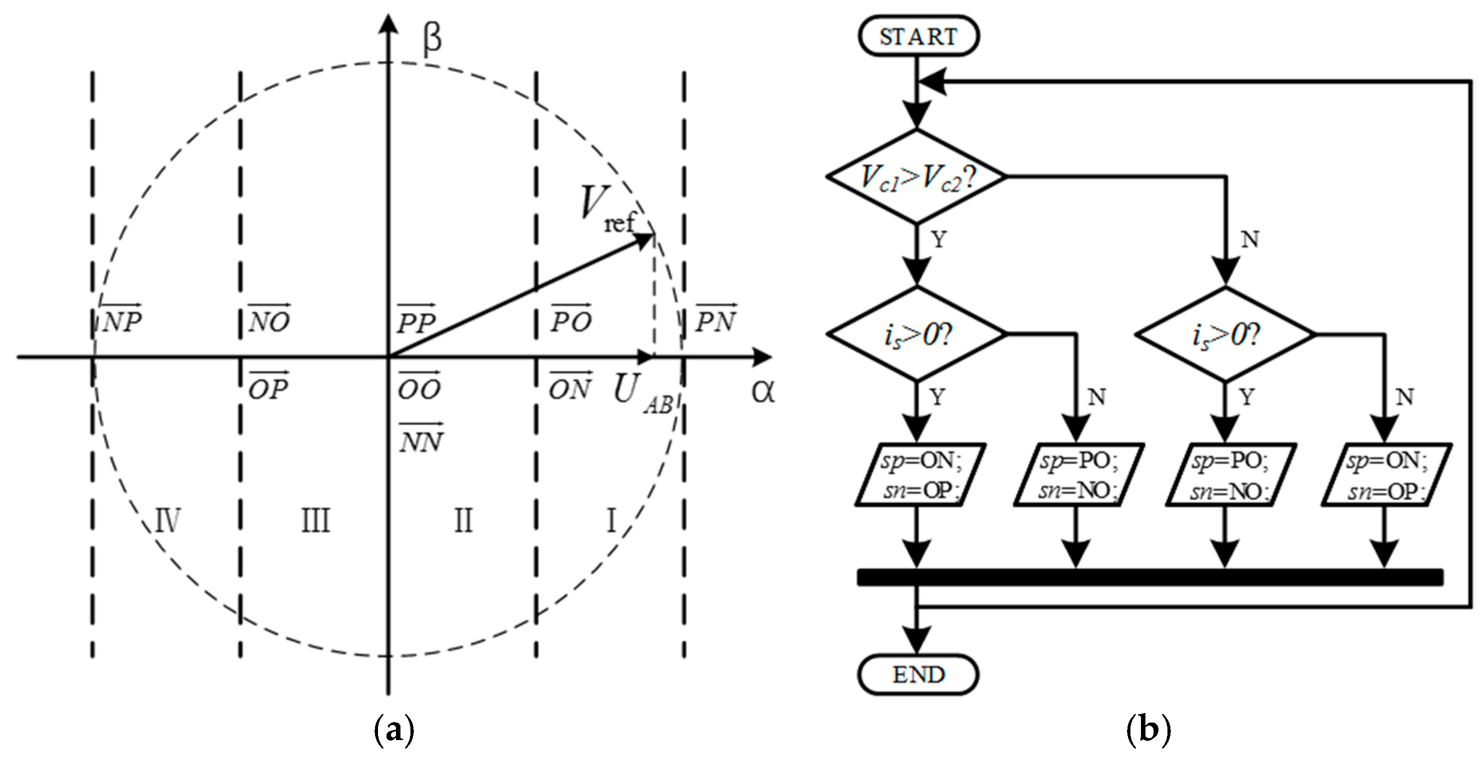
To choose the proper switching states for the 3L-NPC, the single-phase three-level space vector diagram is divided into four sections. The two voltage vectors are selected to synthesize according to the section in which it is located. As shown in Figure 4a, assuming , the voltage is the projection of the vector on the α-axis, and the length of the vector . The vector is rotated counterclockwise at the angular frequency , where in the range of 0–1 is the modulation ratio.
The reference voltage is synthesized by two adjacent vectors. The vector with fewer levels is defined as a small vector , and the vector with a large number of levels is defined as a big vector . The two adjacent switching state vectors are selected to calculate on-durations via Equation (5) under the volt-second balance principle.
is the reference voltage of the modulation wave, is the period of the carrier, is the operational time of , is the operational time of .
As shown above in Table 1, the large vector and zero vector will not cause dc-link capacitor voltage unbalance; however, the small vector causes a fluctuation of neutral point voltage. When the small vector is working, one of the two capacitors is charged or discharged, while the other maintains the same voltage. The small positive vector PO(ON) and small negative vector OP(NO) have opposite effects on the neutral point voltage, so the control of the neutral point voltage can be achieved by choosing a redundant vector.
To analyze the direction of the current flowing through the capacitor, a strategy for solving the fluctuation of the neutral point voltage by using different redundant vectors is shown in Table 2 and Figure 4b. According to the capacitor voltage and grid current, there are four kinds of redundant switch state selections. When none of the redundant vectors are working and the terminal voltage is , the strategy can choose between States PO and ON(sp). Similarly, when terminal voltage is , the strategy can choose between States OP and NO(sn). The result of choosing redundant vectors will be put into a register sp(sn), and the state of the register will be sent to synthesize the switching state finally. When any one of those four redundant vectors is working, the state of register sp(sn) remains unchanged. For example, in Figure 4b, when the system starts to work, and ; if the terminal voltage is , then sp will be ON; if the terminal voltage is , the sn will be OP.
4. Simulation
In order to verify the system’s control strategy adopted above, a 3L-NPC single-phase rectifier shown in Figure 1 is used to conduct a simulation by MATLAB/SIMULINK in this paper, and the simulation parameters are listed in Table 3.
The dynamic response of the system is shown in Figure 5. when load is on or off, output voltage recovers to 400 V within 0.15 s. Input voltage and current is in the same phase; that is, the power factor of the system is close to 1. The bottom of Figure 5 is the terminal voltage. As mentioned earlier, the voltage of two dc-side capacitances, if not controlled, would be unbalanced, which in turn would increase the harmonic component in the output voltage and increase the voltage applied on the power switch transistor, even damage the device or dc-side capacitor. Figure 6 shows the changes in the voltage of the two capacitors. There is no voltage equalizing strategy during the 0–0.3 s period, the maximum value of voltage difference between the two capacitors reached 400 V, and after 0.3 s, the voltage difference gradually disappeared as a voltage equalizing strategy is adopted.
5. Experiment Results
5.1. Prototype
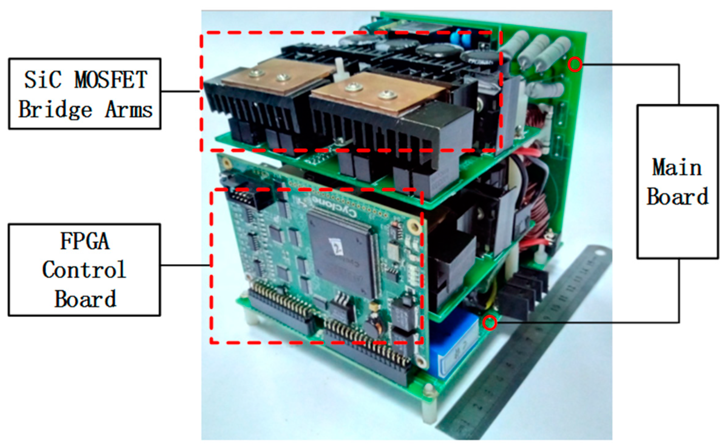
In order to realize the target mentioned above, which includes a control algorithm and high power density, an experimental prototype of the single-phase three-level rectifier was developed. The system is shown in Figure 7. It is divided into three parts. The first part consists of two SiC MOSFET bridge arms and a drive circuit. The drive circuit is designed to drive SiC MOSFET stably. The second part consists of an input inductor, an EMI filter, a voltage sensor and a current sensor, a relay, and a secondary filter. The input inductor is designed to filter the grid voltage harmonic and store power. The EMI filter is designed to filter out high frequency noise and interference signals contained in the grid while keeping electromagnetic radiation generated by the system from leaking to the grid. The input voltage (), grid current (), and dc-link voltage () are detected by sensors as the feedback. Each state of the system is transformed precisely through the switching of the relay. The third part is the FPGA control board, which is designed to control the whole system.
We also have protection methods in our program. If the input voltage or grid current are higher or lower than the expected value limits, the output voltage is not in the setting limits, and the system would be shut down in case heat issues or hazards occur.
The configuration of the control system is shown in Figure 3a. All control algorithms are implemented by Verilog-HDL (Hardware Description Language), one of the universal IEEE industry standard hardware description languages used to describe digital systems and design hardware realization using code methods.
5.2. Experiment Results
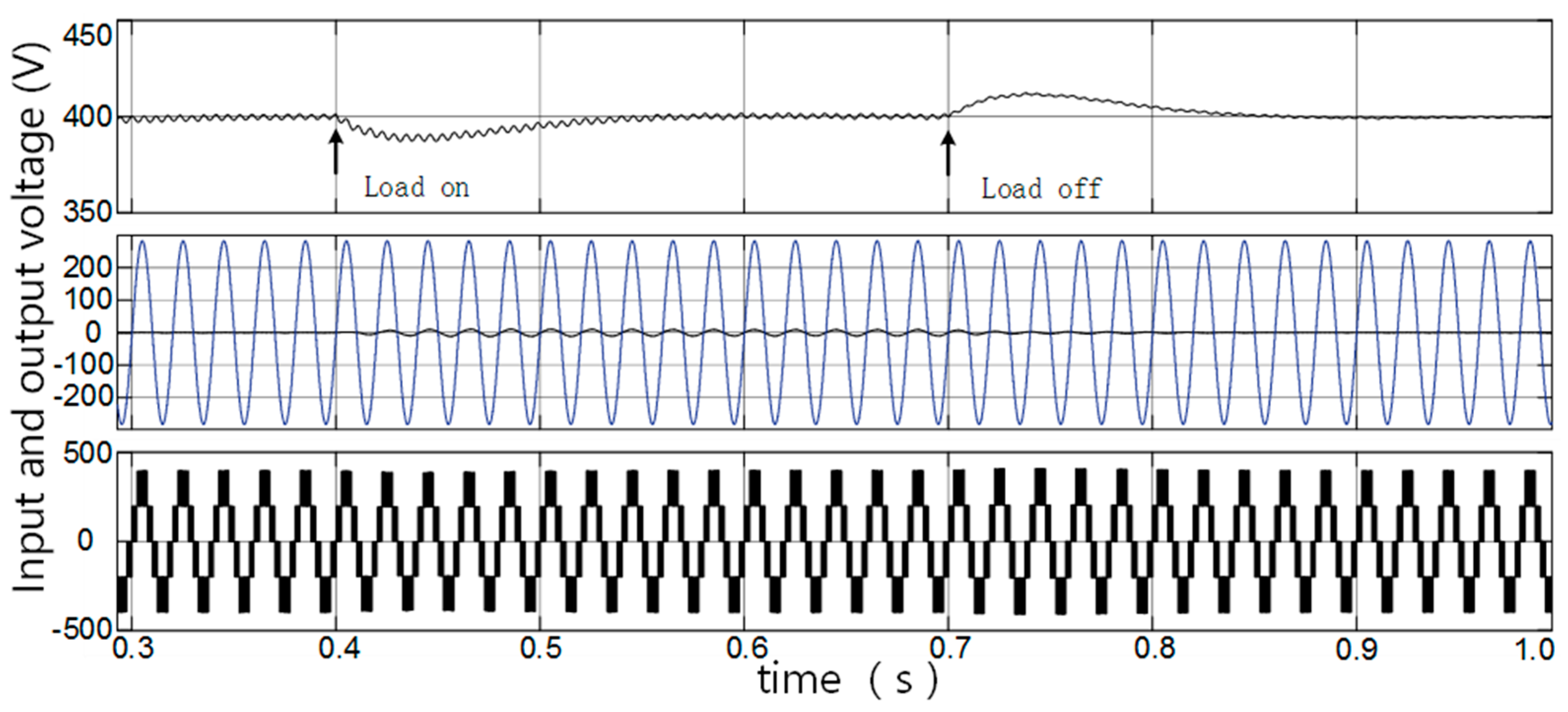
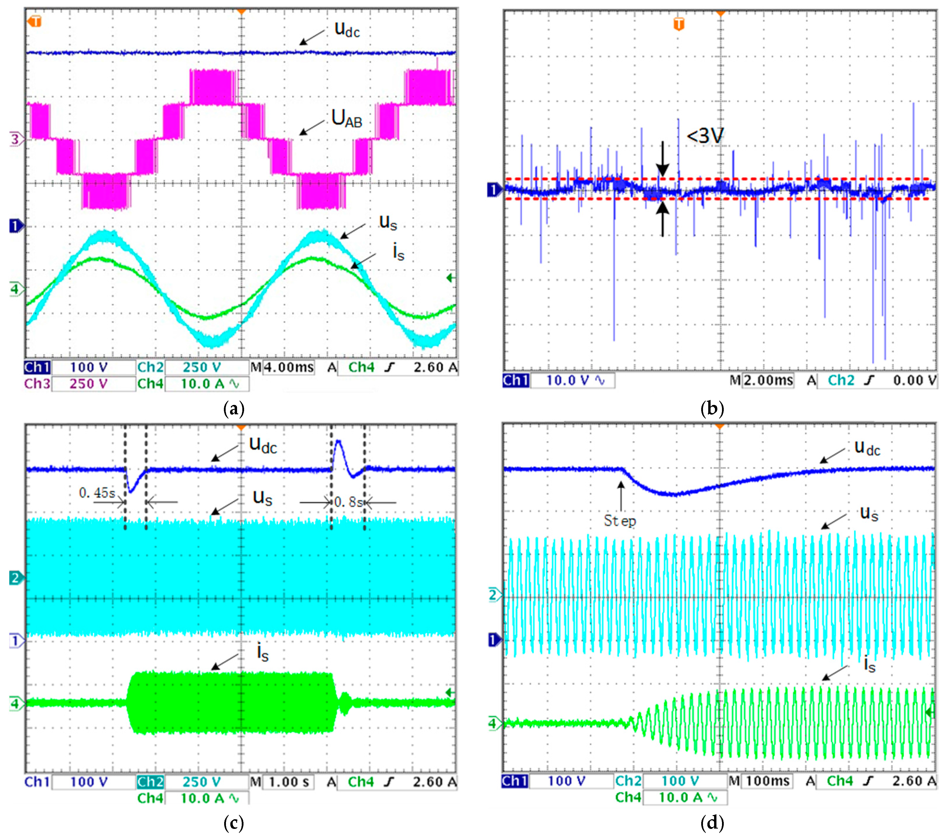
In Figure 8a, the dc-link voltage (), terminal voltage (), input voltage (), and grid current () are illustrated. is stable at 400 V, and and are in the same phase, so the rectifier works within unity-power factor limits. The waveform of presents a low THD in the condition of full load (1.3 kW). Figure 8b presents the ripple of the output voltage, which is lower than 3 V. Figure 8c exhibits the dc-link voltage (), input voltage (), and grid current () when load step changes happen, the recovers to the reference voltage within 0.8 s after the load step changes. Figure 8d shows that the input voltage () and grid current () recover to sinusoidal waveforms immediately after the load step changes. All these experiments illustrate that the system has high dynamic responses.
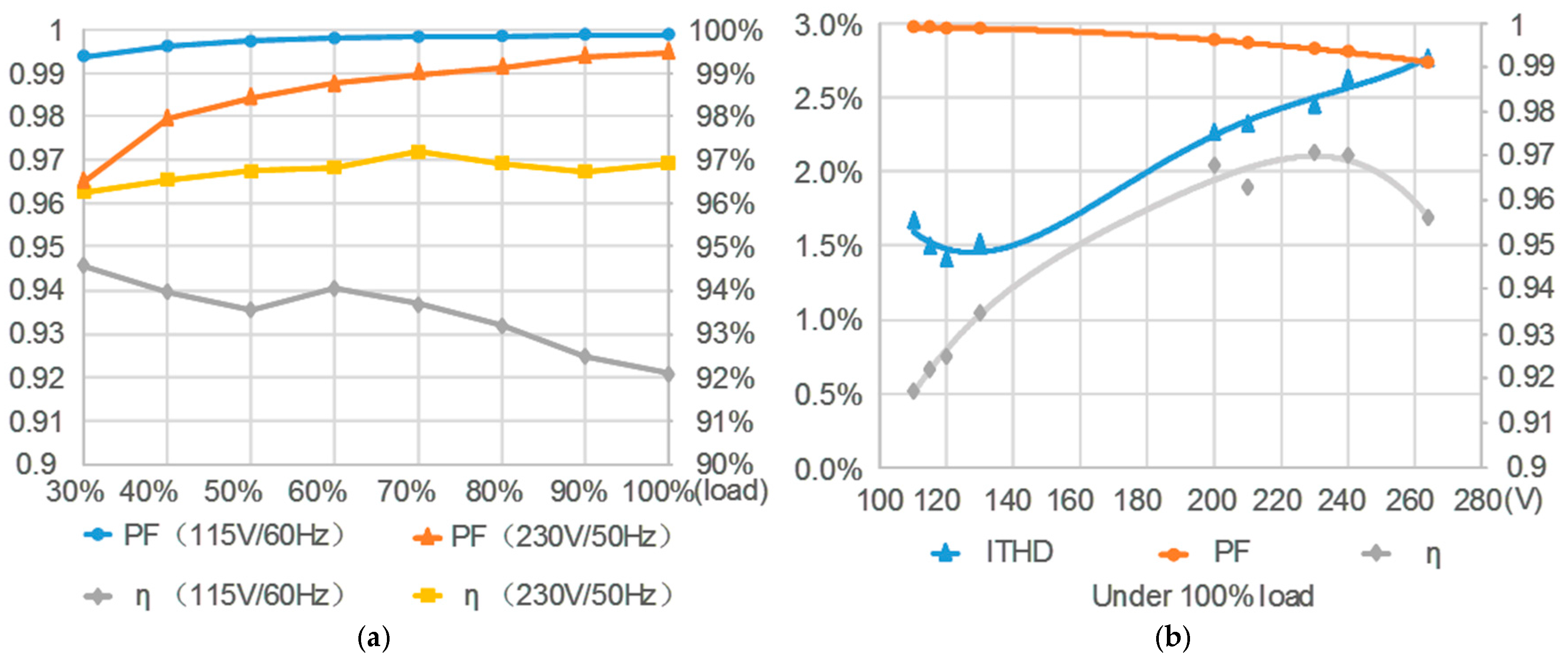
Figure 9a shows the changes in the power factor (PF) and the efficiency when the rectifier works at two different input voltages (115 V/60 Hz and 230 V/60 Hz). In the first case (115 V/60 Hz), the PF reaches 0.995 at the 30% load. Then, the PF increases gradually as the load increases. The PF comes to the maximum (nearly 0.999) when the rectifier is under full load. As for the efficiency, the PF starts at 94.5% under 30% load, then it declines slightly to the 93.5% with 50% load. After that, the efficiency keeps relatively steady until the load increases to 70%. However, it falls dramatically as the load rises. The efficiency achieves the lowest point at the full load. In the second case (230 V/60 Hz), the PF goes up from 0.965 to 0.993 as the PF of the first case, and the efficiency fluctuates between 0.963 and 0.972 through the process of load changing. Generally, PF increases as the load of the rectifier increases and the PF retains a high value. The efficiency ranges from 0.92 to 0.972, which indicates the efficiency has no strong correspondence with the load changes.
The experiment test has been done under the same power level (1.3 kW), and the result is shown in Figure 9b. The PF drops from 0.999 to 0.99 when the input voltage increases from 115 V to 264 V, which coincides with Figure 9a. As the input voltage gains, the input current decreases correspondingly. As for the THD, the PF starts at 1.7% with a 115 V input voltage. Then, it drops drastically to 1.4% when the input voltage is 120 V. Afterwards, the THD increases to 2.7% when the input voltage increases to 264 V. In terms of the efficiency, the PF begins at 0.92, and then improves sharply to 0.965 when the input voltage reaches 200 V. After the light rolling of the efficiency between 200 and 240 V, a slight drop appears at 264 V input voltage.
Moreover, a comparison experiment between the Si device and the SiC device is developed, and the operation frequency of Si IGBT is 3 kHz, while the operation frequency of SiC MOSFET is 30 kHz. The experiment result is shown in Figure 9c,d. The ITHD of the SiC system is lower than the Si system at the same input voltage with an increased switching frequency, and the PF of the SiC system is higher than that of the Si system and almost close to 1 in different input voltage conditions.
The experiments and the test above verify that the SiC MOSFET single-phase three level rectifier can work with a high efficiency, a low THD, and a unity power factor.
6. Conclusions
A high-power-density single-phase 3L-NPC rectifier was built. Its size is shown in Figure 7, and the power density is relatively high. Through the adoption of a transient current control strategy, the SVPWM method, and a redundant vector selection strategy, the goal of a stable dc-link voltage, a high power factor, a low THD, and a relatively high efficiency is achieved. The dynamic characteristics of the system were tested, and the system was found to have a high dynamic response. The grid voltage and current quickly adjust to recover sinusoidal waveforms. The superior advantages of SiC MOSFET in breakdown voltage, heat conductivity, and high temperature compared to Si MOSFET are reflected in the high efficiency of the 3L-NPC rectifier built here.
Acknowledgments
This work was supported by the National Natural Science Foundation of China (Grant Nos. 51377004 and 51477144).
Author Contributions
Tao Zhou and Zeliang Shu designed the control algorithm, the controller, and the main circuits; Tao Zhou, Deng Luo, Xiaoxiao Guo, and Yajun Chen designed the prototype and achieved the experiments; Hongjian Lin analyzed the data.
Conflicts of Interest
The authors declare no conflict of interest.
References
- Peng, H.; Hagiwara, M.; Akagi, H. Modeling and analysis of switching-ripple voltage on the DC Link between a diode rectifier and a modular multilevel cascade inverter (MMCI). IEEE Trans. Power Electron. 2013, 28, 75–84. [Google Scholar] [CrossRef]
- Gautam, S.P.; Kumar, L.; Gupta, S. Hybrid topology of symmetrical multilevel inverter using less number of devices. IET Power Electron. 2015, 8, 2125–2135. [Google Scholar] [CrossRef]
- Kouro, S.; Malinowski, M.; Gopakumar, K.; Pou, J.; Franquelo, L.G.; Wu, B.; Rodriguez, J.; Perez, M.A.; Leon, J.I. Recent advances and industrial applications of multilevel converters. IEEE Trans. Ind. Electron. 2010, 57, 2553–2580. [Google Scholar] [CrossRef]
- He, X.; Shu, Z.; Peng, X.; Zhou, Q.; Zhou, Y.; Zhou, Q.; Gao, S. Advanced cophase traction power supply system based on three-phase to single-phase converter. IEEE Trans. Power Electron. 2014, 29, 5323–5333. [Google Scholar] [CrossRef]
- Shu, Z.; Zhu, H.; He, X.; Ding, N.; Jing, Y. One-inductor-based auxiliary circuit for dc-link capacitor voltage equalization of diode-clamped multilevel converter. IET Power Electron. 2013, 6, 1339–1349. [Google Scholar] [CrossRef]
- Zhu, H.; Shu, Z.; Gao, F.; Qin, B.; Gao, S. Five-level diode-clamped active power filter using voltage space vector-based indirect current and predictive harmonic control. IET Power Electron. 2014, 7, 713–723. [Google Scholar] [CrossRef]
- He, X.Q.; Guo, A.P.; Peng, X.; Zhou, Y.Y.; Shi, Z.H.; Shu, Z.L. A traction three-phase to single-phase cascade converter substation in an advanced traction power supply system. Energies 2015, 8, 9915–9929. [Google Scholar] [CrossRef]
- Shu, Z.; Ding, N.; Chen, J.; Zhu, H.; He, X. Multilevel SVPWM with DC-Link capacitor voltage balancing control for diode-clamped multilevel converter based STATCOM. IEEE Trans. Ind. Electron. 2013, 60, 1884–1896. [Google Scholar] [CrossRef]
- Xu, P.; He, X.Q.; Han, P.C.; Guo, A.P.; Shu, Z.L.; Gao, S.B. Smooth Switching Technique for Voltage Balance Management Based on Three-Level Neutral Point Clamped Cascaded Rectifier. Energies 2016, 9, 803. [Google Scholar] [CrossRef]
- Anthon, A.; Zhang, Z.; Andersen, M.A.E.; Holmes, D.G.; McGrath, B.; Teixeira, C.A. The Benefits of SiC MOSFETS in a T-Type Inverter for Grid-Tie Applications. IEEE Trans. Power Electron. 2017, 32, 2808–2821. [Google Scholar] [CrossRef]
- Hazra, S.; Madhusoodhanan, S.; Moghaddam, G.K.; Hatua, K.; Bhattacharya, S. Design Considerations and Performance Evaluation of 1200-V 100-A SiC MOSFET-Based Two-Level Voltage Source Converter. IEEE Trans. Ind. Appl. 2016, 52, 4257–4268. [Google Scholar] [CrossRef]
- Chen, Z.; Yao, Y.; Boroyevich, D.; Ngo, K.D.T.; Mattavelli, P.; Rajashekara, K. A 1200-V, 60-A SiC MOSFET Multichip Phase-Leg Module for High-Temperature, High-Frequency Applications. IEEE Trans. Power Electron. 2014, 29, 2307–2320. [Google Scholar] [CrossRef]
- Mainali, K.; Tripathi, A.; Madhusoodhanan, S.; Kadavelugu, A.; Patel, D.; Hazra, S.; Hatua, K.; Bhattacharya, S. A Transformerless Intelligent Power Substation: A three-phase SST enabled by a 15-kV SiC IGBT. IEEE Power Electron. Mag. 2015, 2, 31–43. [Google Scholar] [CrossRef]
- Han, D.; Sarlioglu, B. Comprehensive Study of the Performance of SiC MOSFET-Based Automotive DC–DC Converter under the Influence of Parasitic Inductance. IEEE Trans. Ind. Appl. 2016, 52, 5100–5111. [Google Scholar] [CrossRef]
- Jahdi, S.; Alatise, O.; Gonzalez, J.A.O.; Bonyadi, R.; Li, R.; Mawby, P. Temperature and Switching Rate Dependence of Crosstalk in Si-IGBT and SiC Power Modules. IEEE Trans. Ind. Electron. 2016, 63, 849–863. [Google Scholar] [CrossRef]
Figure 1.
(a) Circuit configuration of 3L-NPC; (b) five-level waveform of terminal voltage.
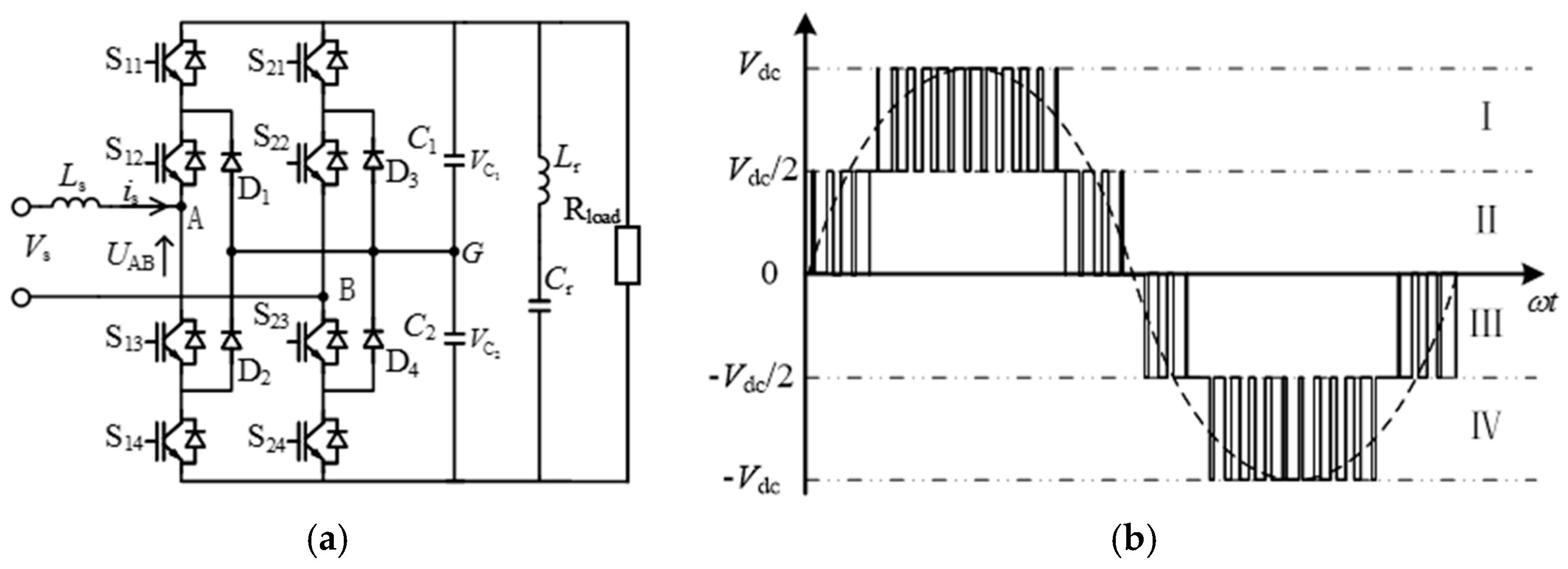
Figure 2.
(a–i) The nine switching states of the single-phase three-level rectifier.

Figure 3.
(a) Control algorithm; (b) transient current control strategy.
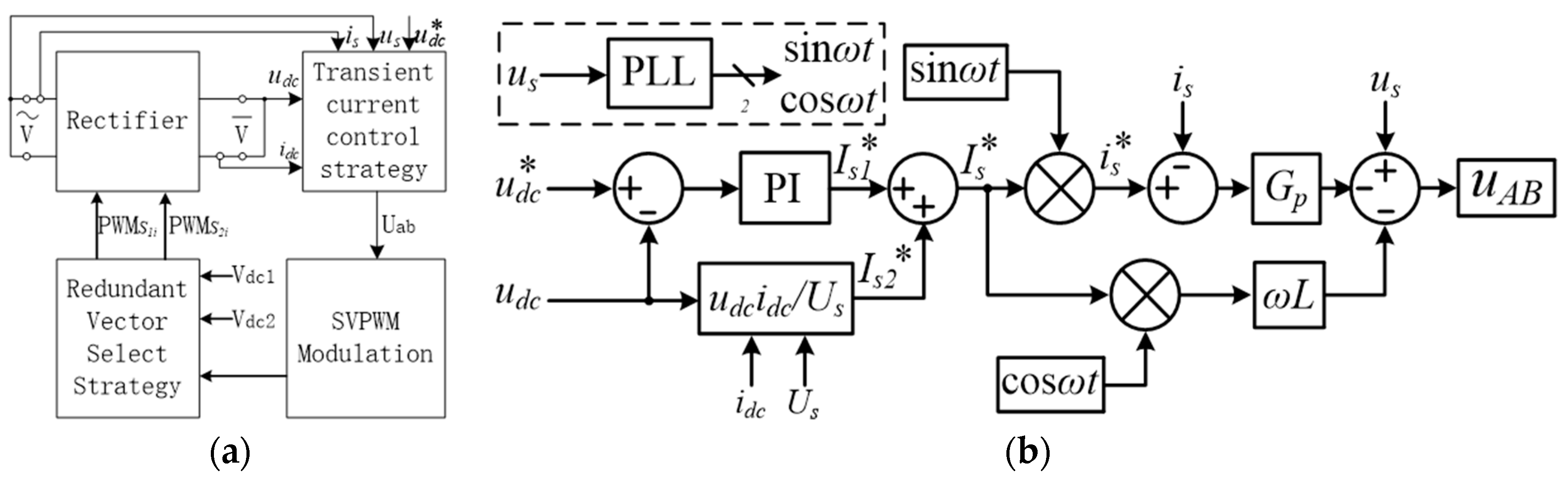
Figure 4.
(a) SVPWM reference voltage; (b) redundant vector selection procedure.

Figure 5.
DC-link voltage, input voltage, and current and terminal voltage.

Figure 6.
The DC capacitors voltages with and without equalization control.
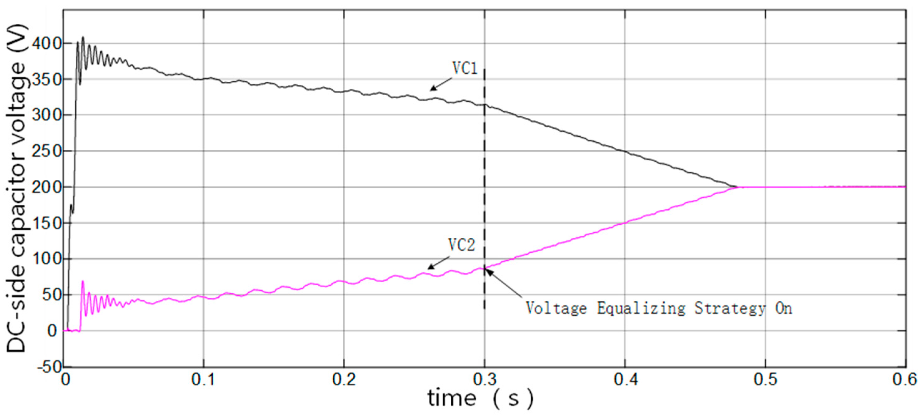
Figure 7.
Prototype of the system.

Figure 8.
Experiment results. (a) State–state waveforms; (b) output voltage ripple; (c) dynamic waveforms with and without load; (d) detail waveforms at load step change.
Figure 8.
Experiment results. (a) State–state waveforms; (b) output voltage ripple; (c) dynamic waveforms with and without load; (d) detail waveforms at load step change.

Figure 9.
Experimental statistics: (a) power factor and efficiency; (b) THD, power factor, and efficiency with 100% load; (c) THD comparison between Si and SiC devices; (d) PF comparison between Si and SiC devices.
Figure 9.
Experimental statistics: (a) power factor and efficiency; (b) THD, power factor, and efficiency with 100% load; (c) THD comparison between Si and SiC devices; (d) PF comparison between Si and SiC devices.


Table 1.
Switch state and effect on two capacitors. : charge; : discharge; : no effect; Z: zero vector; SP: small positive vector; LP: large positive vector; SN: small negative vector; LN: large negative vector.
Table 1.
Switch state and effect on two capacitors. : charge; : discharge; : no effect; Z: zero vector; SP: small positive vector; LP: large positive vector; SN: small negative vector; LN: large negative vector.
| State | Vector Categories | |||||
|---|---|---|---|---|---|---|
| 1 | P | P | 0 | Z | ||
| 2 | P | O | SP | |||
| 3 | P | N | + | LP | ||
| 4 | O | P | SN | |||
| 5 | O | O | 0 | Z | ||
| 6 | O | N | SP | |||
| 7 | N | P | LN | |||
| 8 | N | O | SN | |||
| 9 | N | N | 0 | Z |
Table 2.
Redundant vector selection.
| Terminal Voltage | Relation | Current Direction | Vector Selected | Result |
|---|---|---|---|---|
| A→B | ||||
| B→A | ||||
| A→B | ||||
| B→A | ||||
| A→B | ||||
| B→A | ||||
| A→B | ||||
| B→A |
Table 3.
System and control parameters.
| Parameters | Values |
|---|---|
| Input AC Voltage | 115 V–264 V |
| Input Current | 15 A (Max) |
| Input AC Voltage Frequency | 47 Hz–63 Hz |
| Output DC Voltage | 400 V |
| Output Power | 1.3 kW (Max) |
| Power Density | 0.56 W/cm3 |
| The Inductance of Input Side | 0.4 mH |
| Filter Circuit | 3 mF/0.84 mH |
| Switching Frequency | 30 kHz |
© 2017 by the authors. Licensee MDPI, Basel, Switzerland. This article is an open access article distributed under the terms and conditions of the Creative Commons Attribution (CC BY) license (http://creativecommons.org/licenses/by/4.0/).
Share and Cite
MDPI and ACS Style
Zhou, T.; Shu, Z.; Lin, H.; Luo, D.; Chen, Y.; Guo, X. A High-Power-Density Single-Phase Rectifier Based on Three-Level Neutral-Point Clamped Circuits. Energies 2017, 10, 697. https://doi.org/10.3390/en10050697
AMA Style
Zhou T, Shu Z, Lin H, Luo D, Chen Y, Guo X. A High-Power-Density Single-Phase Rectifier Based on Three-Level Neutral-Point Clamped Circuits. Energies. 2017; 10(5):697. https://doi.org/10.3390/en10050697
Chicago/Turabian StyleZhou, Tao, Zeliang Shu, Hongjian Lin, Deng Luo, Yajun Chen, and Xiaoxiao Guo. 2017. "A High-Power-Density Single-Phase Rectifier Based on Three-Level Neutral-Point Clamped Circuits" Energies 10, no. 5: 697. https://doi.org/10.3390/en10050697
Note that from the first issue of 2016, this journal uses article numbers instead of page numbers. See further details here.