Theoretical and Experimental Investigation of Switching Ripple in the DC-Link Voltage of Single-Phase H-Bridge PWM Inverters


Department of Electrical, Electronic and Information Engineering, University of Bologna, Viale Risorgimento 2, 40136 Bologna, Italy
*
Author to whom correspondence should be addressed.
Energies 2017, 10(8), 1189; https://doi.org/10.3390/en10081189
Submission received: 27 July 2017
/
Revised: 8 August 2017
/
Accepted: 9 August 2017
/
Published: 11 August 2017
Abstract
:Direct current (DC)-link voltage ripple analysis is essential for determining harmonic noise and for DC-link capacitor design and selection in single-phase pulse-width modulation (PWM) inverters. This paper provides an extensive theoretical analysis of DC-link voltage ripple for full-bridge (H-bridge) inverters, with simulation and experimental verifications, considering a DC source impedance (non-ideal DC voltage source). The DC voltage ripple amplitude is theoretically estimated as a function of the output current, both amplitude and phase angle, and the modulation index. It consists of a switching frequency component and a double-fundamental frequency component (i.e., 100 Hz), thereby both components are considered in the analysis. In particular, the peak-to-peak distribution, maximum amplitude, and root mean square (RMS) values of the voltage switching ripple over the fundamental period are obtained. Based on the DC voltage requirements, simple and effective guidelines for designing DC-link capacitors are obtained.
1. Introduction
The full-bridge (H-bridge) inverter is the basic configuration used for single-phase direct current (DC)/alternating current (AC) power conversion. It can also be easily extended to multiphase and multilevel configurations, obtaining different output voltage levels. The single-phase configuration is used in many low-power applications (i.e., up to 5–10 kW), either grid connected or stand-alone, with special emphasis on the interface of renewable energy sources in distributed generation systems, such as photovoltaic (PV) power plants [1,2,3]. Since the performance of an inverter mainly depends on its modulation strategy, many carrier-based pulse-width modulation (PWM) techniques have been developed in the last decades [4,5,6]. The performance is evaluated by the total harmonic distortion (THD) of the input/output voltages and currents, switching losses, and efficiency.
Recently, there has been much work on inverter output voltage and output current characteristics considering PWM techniques. Simple and effective expressions for determining the peak-to-peak output current ripple amplitude over the modulation index range, for two- and multilevel inverters, are presented in [7,8,9]. An extension to multiphase inverters and a comparison among the cases with different phase numbers is presented in [10]. In [11], the analytical time-averaging approach is applied to a single-phase cascaded multilevel PWM inverter. The current quality is evaluated in the time domain by using the output current ripple normalized mean square (NMS) criterion.
However, a few analyses have been performed on estimating the inverter input (DC-link) characteristics, and in particular the DC voltage. Analyzing the inverter input side is important for DC-link capacitor design and selection in voltage source inverters (VSIs), since it contributes to the cost, size, and failure rate on a considerable scale. In order to satisfy more stringent reliability constraints, DC-link capacitors face a few challenges. Some of them are reduction of weight and volume, reliability, being exposed to more harsh environments (high ambient temperature, high humidity, etc.) in emerging applications, prevention of overheating, and extension of life time [12,13]. In order to overcome the above challenges, it is necessary to carry out a detailed analysis of DC-link current and voltage ripples.
With reference to three-phase inverters, the developments related to input current and voltage characteristics are usually based on a Fourier analysis (harmonics) and root mean square (RMS) calculations. The RMS value of the DC-link capacitor current in three-phase voltage source PWM inverters is calculated by using the time domain approach in [14,15]. For synthesizing the DC-link current, only the fundamental component of the line current is considered, and the effect of the line current ripple is neglected. The fundamental and ripple line current components are presented together in [16,17]. In all of those papers, a balanced three-phase load is assumed for the DC-link current’s analytical calculations. A variety of analytical approaches for the single- and three-phase voltage source inverters determining the DC-link current harmonics for any kind of modulation strategy based on a double Fourier analysis are presented in [18,19,20,21].
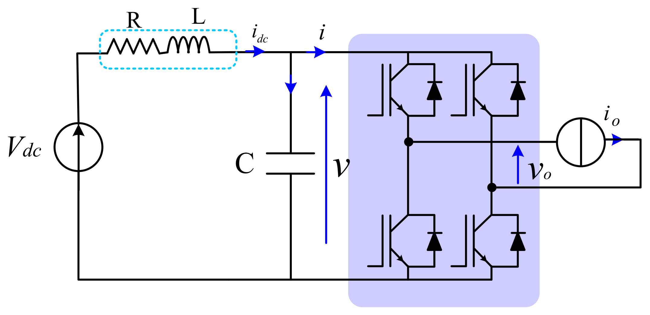
Generally speaking, the DC-link voltage ripple in single-phase inverters can be expressed considering three different components: the DC (average) component, the low-frequency component (double-fundamental frequency, 100 Hz), and the high-frequency component (switching, many kHz). In the literature, developments are usually focused on one of these components, neglecting the impact of the other two. In many applications, even if the DC supply is an almost ideal voltage source (having small equivalent impedance), only the low-frequency voltage ripple components are negligible, whereas the switching frequency components become relevant in the case of small DC capacitors. The low-frequency voltage ripple components can be relevant in the case of photovoltaic DC supply (high DC series resistance, R) or a DC-link inductive filter (high DC series reactance, ωL), as represented in basic circuit scheme of Figure 1.
In [22], the analysis of and calculations for DC-link current and voltage low-frequency ripples under balanced and unbalanced loads for three-phase VSIs are presented. In particular, DC-link average and harmonic RMS currents are calculated, and DC-link voltage ripple under the unbalanced load is obtained considering only the double-fundamental frequency component, but the switching frequency voltage ripple has been examined shortly.
A preliminary theoretical analysis of DC-link voltage ripple, considering both the switching frequency and double-fundamental frequency components, has been presented by the authors in [23], for a single-phase H-bridge PWM inverter. This paper further develops and completes the work [23], also providing a complete set of experimental results taken in different operating conditions. Detailed analytical expressions for the peak-to-peak DC voltage ripple amplitude distribution over the fundamental period are reviewed, together with the maximum peak-to-peak amplitude and RMS values of the voltage switching ripple component. Comprehensive simulation and experimental tests confirmed the validity of the theoretical developments.
2. Analysis of the Inverter Input Characteristics
2.1. System Configuration
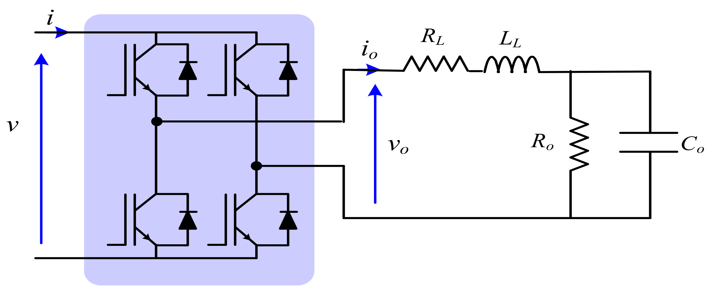
Figure 1 shows the basic circuit scheme of a typical single-phase H-bridge inverter configuration. The inverter is connected to a constant DC voltage supply (Vdc) via a DC source impedance consisting of resistance (R) and/or inductance (L). These parameters represent the equivalent series impedance of the DC source. In parallel with the modelled DC source, a DC-link capacitor (C) is connected to smooth the voltage ripple. The load is represented by a sinusoidal AC output current (io), meaning the inverter supplies either a passive load or is being connected to the electrical grid with a negligible switching current ripple.
Using the sinusoidal PWM technique, and neglecting the DC-link voltage oscillation compared to its average value (v ≈ V), the inverter output voltage, averaged over the switching period Ts, is calculated within a linear modulation range as
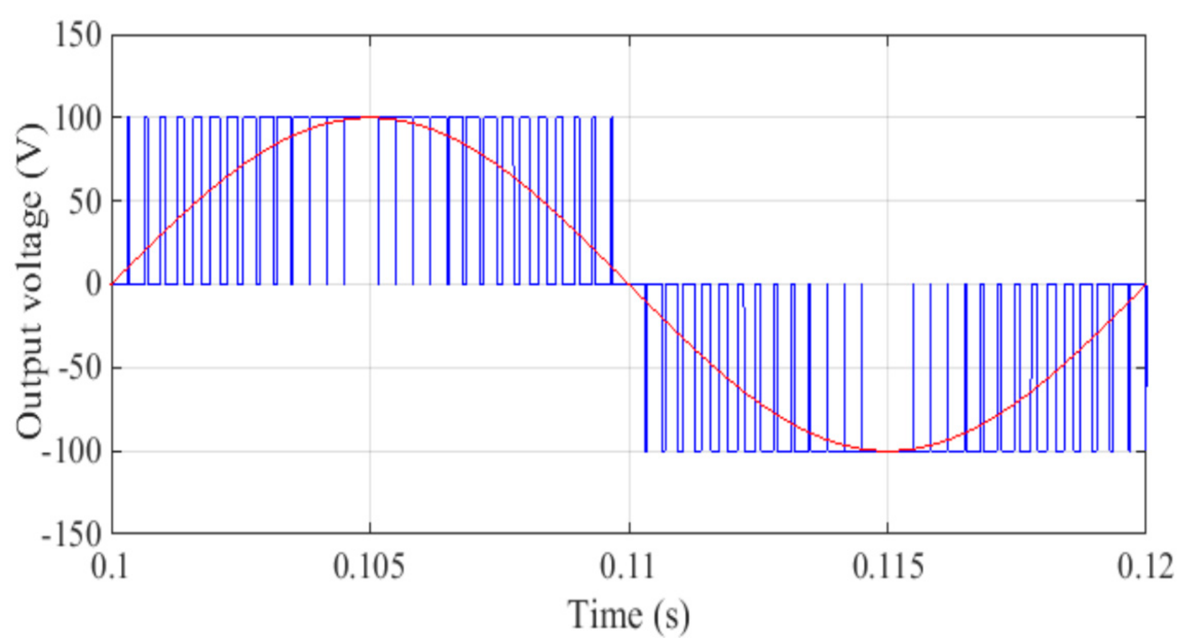
where ϑ = ωt, ω is the fundamental angular frequency (ω = 2π/T), T is the fundamental period, and m is the modulation index (m = Vo/V). When the ratio between the fundamental and switching frequency is high enough, the reference signal is considered constant over one switching period. The output voltage and its fundamental component (averaged value) are represented in Figure 2.
2.2. Input Current Analysis
Neglecting the switching ripple, the inverter output current is expressed as a sinusoid:
being Io the output current amplitude, and ϕ its phase angle compared to the voltage.
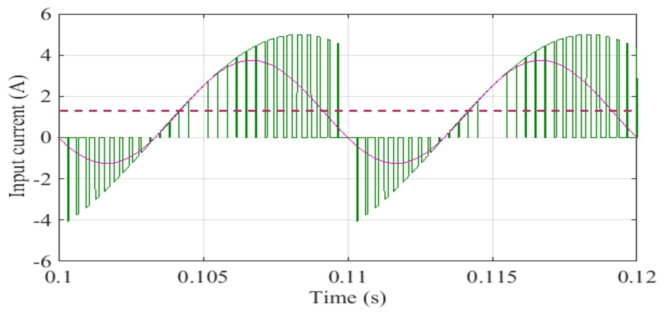
The instantaneous input current i(t), shown in Figure 3, has three relevant components: DC (average) component Idc, alternating double-fundamental frequency component (100 Hz), and switching frequency component ∆i(t):
The input current averaged over the switching period (Ts), representing the low-frequency input current harmonics, can be expressed as:
Neglecting the inverter losses, and supposing the inverter input voltage is almost constant and equal to V, the input/output power balance can be written as:
Introducing Equations (1) and (2) in (5), the averaged input current is calculated as:
The average (DC) and the low-frequency input current components (double-fundamental frequency, 100 Hz), can be simply expressed and readily obtained by Equation (6):
According to Equations (3), (4), (6), and (7), the switching frequency input current component is finally calculated as:
3. Analysis of Input DC-Link Voltage
3.1. Low-Frequency (Averaged) DC-Link Voltage Components
As well as for the current, the instantaneous DC-link voltage consists of three relevant components: DC (average) component V, low-frequency component (2f = 100 Hz) , and switching frequency component ∆v:
The average component V is calculated by subtracting the voltage drop on the series DC supply resistance R (if any) from the DC supply voltage Vdc as:
The low-frequency DC-link voltage component can be simply calculated on the basis of the amplitude of the low-frequency input current component (8) and the DC-link equivalent impedance Z2f, as follows:
being Z2f the parallel between the equivalent DC source impedance and the reactance of the DC-link capacitor, both calculated at the double-fundamental frequency 2f = 100 Hz:
3.2. Switching Frequency DC-Link Voltage Component
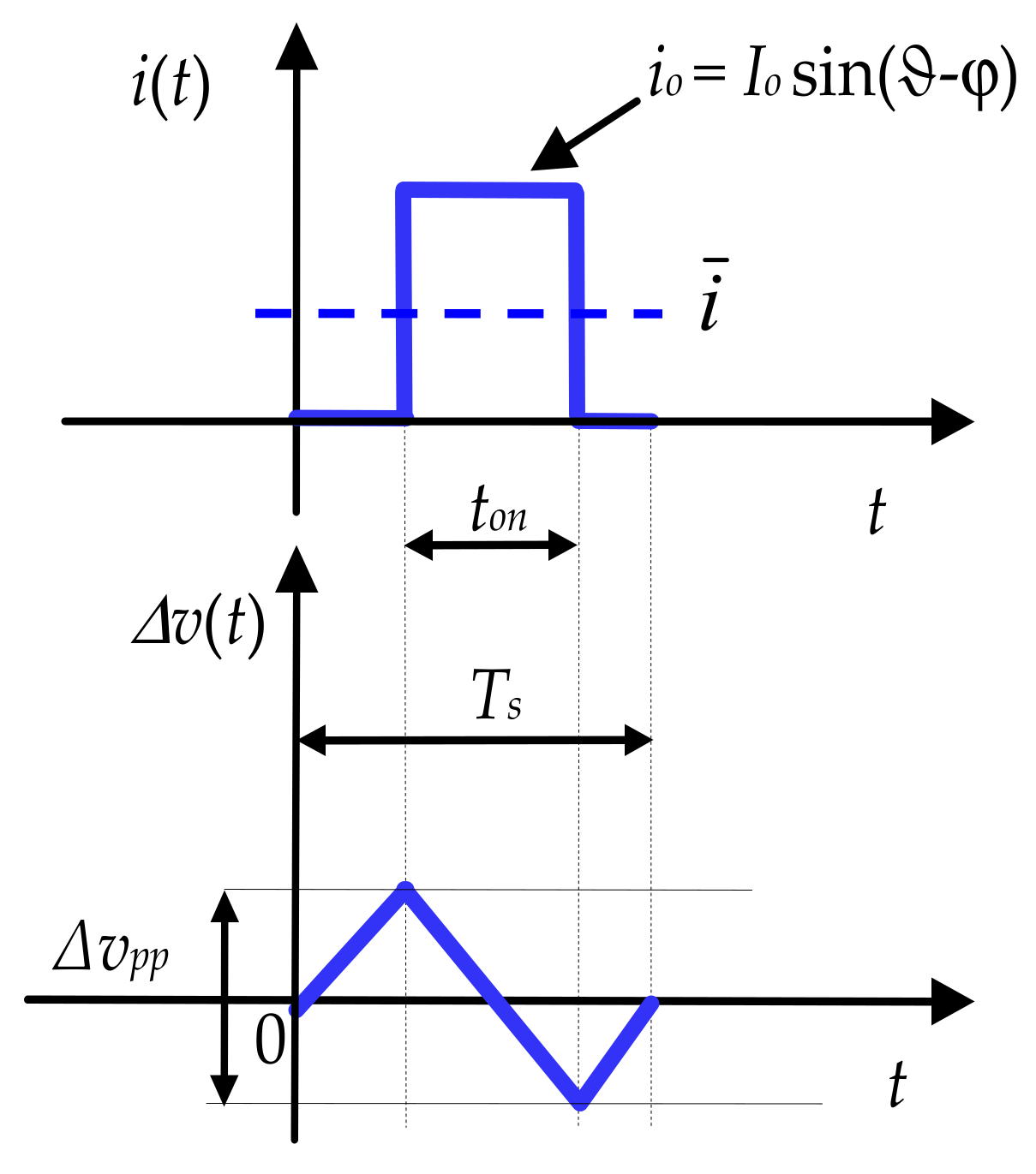
A typical instantaneous input current and voltage are depicted in Figure 4 over the switching period Ts. Considering sinusoidal PWM, the “on-time” interval ton can be calculated as:
Furthermore, neglecting the variation of the low-frequency DC-link voltage component within the switching period Ts (being the switching frequency much higher than the double-fundamental frequency), the peak-to-peak amplitude of the switching frequency DC-link voltage component can be expressed as follows:
In order to obtain the peak-to-peak voltage switching ripple ∆vpp, the input current switching frequency component ∆i has to be determined.
Assuming that the reactance of the DC-link capacitor 1/ωsC dominates the DC source impedance at the switching frequency, the DC-link equivalent impedance becomes:
As a result, the whole switching current component ∆i circulates through the DC-link capacitor, and only the capacitance C determines the amplitude of the voltage switching ripple component. Introducing the “on-time” interval ton calculated in (15), the corresponding peak-to-peak switching voltage ripple over the interval (0–ton) is given by:
Equations (18), (15), and (9) can be utilized in order to calculate the peak-to-peak amplitude of the DC-link voltage switching ripple:
Equation (19) suggests normalization for ∆vpp, as follows:
being the normalized peak-to-peak voltage switching ripple amplitude rpp(m,ϑ,ϕ) expressed as:
3.3. Peak-to-Peak Voltage Ripple Diagrams
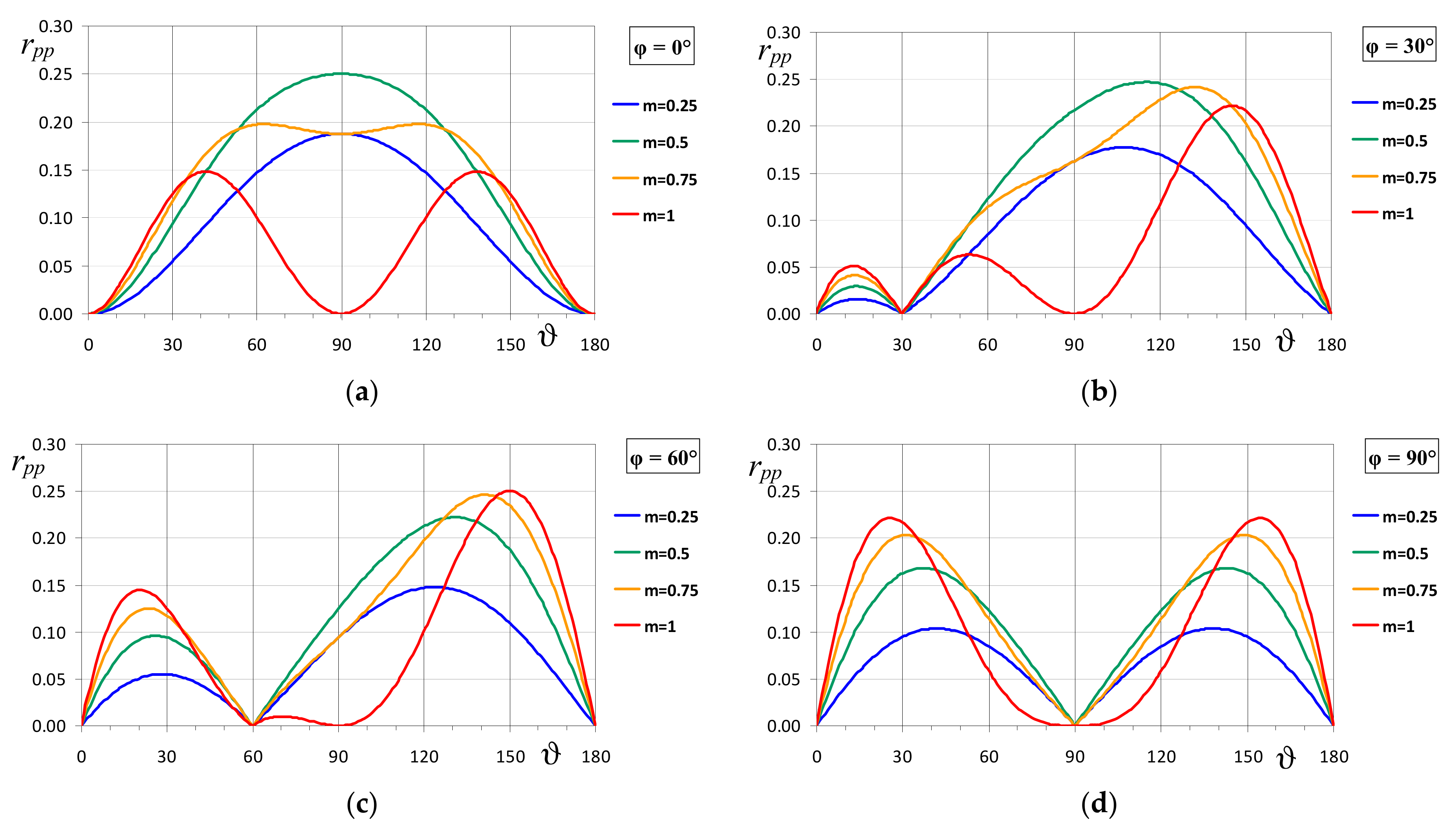
Figure 5 shows the distribution of the normalized peak-to-peak voltage switching ripple amplitude calculated by Equation (21) over the half-fundamental period, i.e., ϑ = (0, 180°). Four modulation indices have been selected in the range m = (0, 1) with the step 0.25. Also, four output phase angles are considered, ϕ = 0, 30°, 60°, and 90°.
According to Figure 5, the normalized voltage switching ripple amplitude rpp(ϑ) varies between 0 (min) and 0.25 (max). In each of those four cases, the rpp(ϑ) minimum and maximum for different m appear at different angles ϑ over the half-fundamental period.
In the case of a unity output power factor (ϕ = 0), as for most of the grid-connected applications, the maximum of the normalized peak-to-peak voltage switching ripple amplitude is obtained from Equation (21), as:
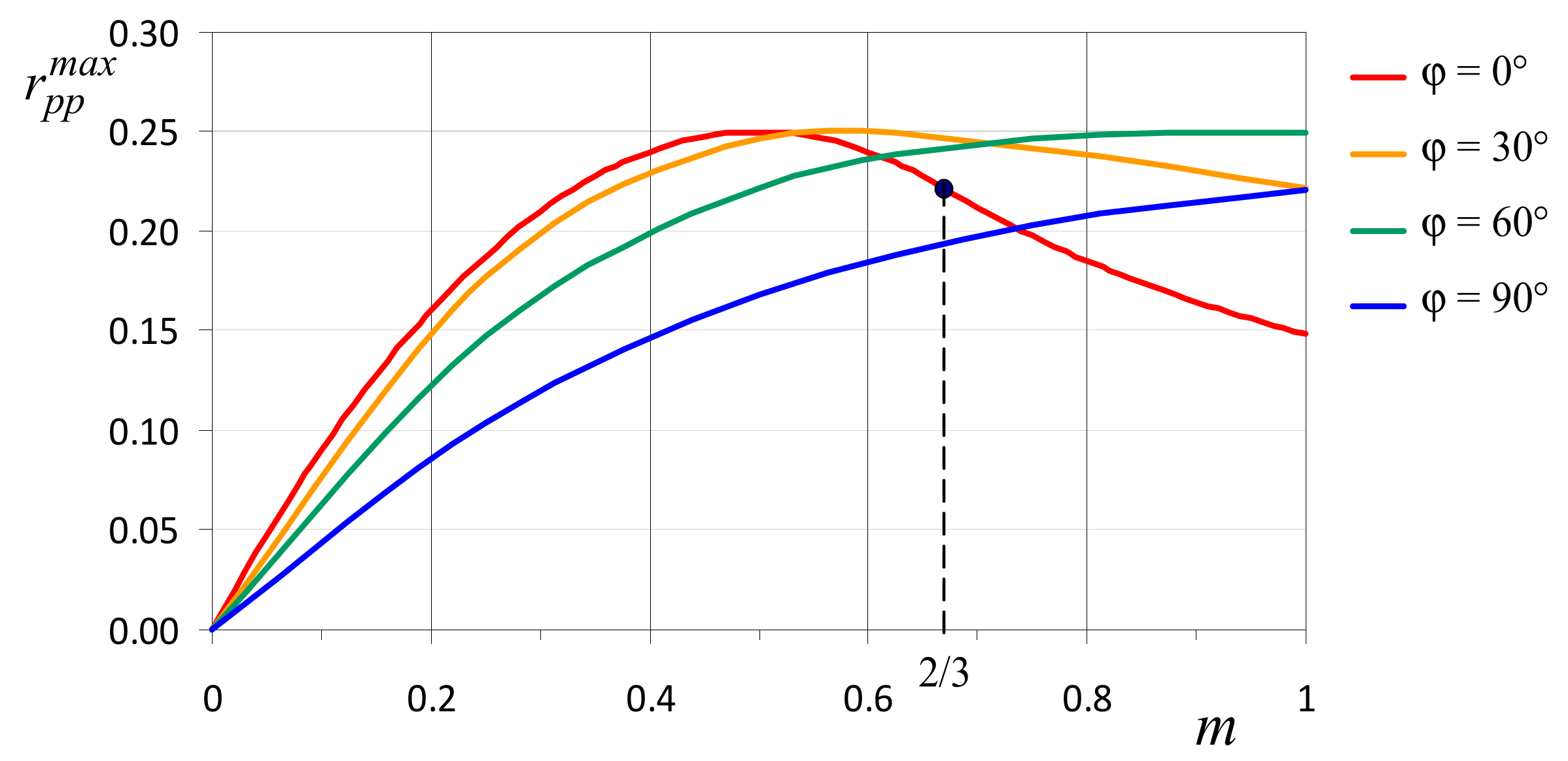
Figure 6 shows the maximum of the normalized peak-to-peak ripple amplitude over the whole modulation index range, for ϕ = 0°, 30°, 60°, and 90°. In the case of ϕ = 0°, was analytically determined by Equation (22) (red trace), while for other three cases it was done numerically.
3.4. RMS of Instantaneous Switching Voltage Ripple
The instantaneous DC-link voltage switching ripple ∆v(t) is a symmetric triangular waveform with the amplitude corresponding to the half of the peak-to-peak ripple envelope (∆vpp/2). The RMS value of the triangular signal ∆Vrms can be easily determined by dividing its peak value by . In the case of variable amplitude, the RMS over a (half) fundamental period can be calculated as:
Introducing Equation (19) into Equation (23), and integrating, yields:
Normalizing Equation (24), similarly to Equations (20) and (21), results in:
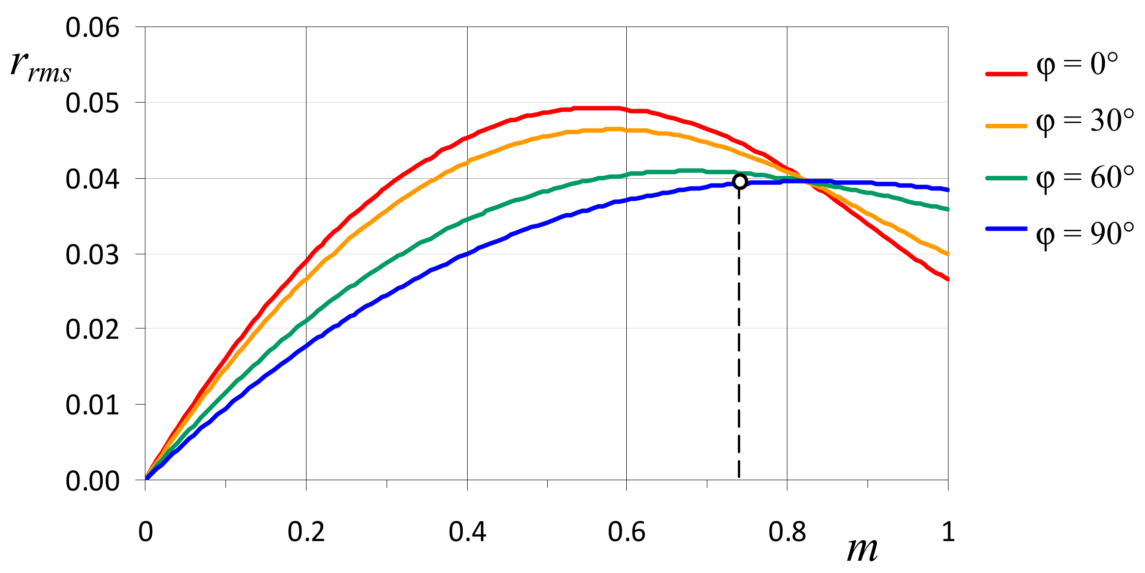
Figure 7 shows the normalized DC-link voltage switching ripple RMS given by Equation (25) as a function of the modulation index for different output phase angles ϕ.
It can be noted that there is one value of the modulation index when rrms becomes completely independent on the output phase angle ϕ, and it depends only on m.
By exploiting Equation (25), this specific value of m corresponds to the following condition:
Solving Equation (26) results in:
Introducing Equation (27) into Equation (25), the corresponding normalized DC-link voltage switching ripple RMS is: rrms (m = 0.825) ≅ 0.04, according to the diagram in Figure 7.
4. Guidelines for Designing the DC-Link Capacitor
Based on the analysis of the DC-link voltage components in Section 3, simple and effective guidelines for designing a DC-link capacitor are proposed in this section. In particular, the DC-link capacitance is calculated taking into account requirements or restrictions referred to in the switching frequency and/or double-fundamental frequency voltage ripple components.
4.1. Capacitor Design Based on Switching Frequency DC-Link Voltage Ripple Requirements
Concerning DC-link voltage ripple at the switching frequency (that is, in the order of kHz), the capacitive reactance 1/ωsC is certainly much lower than the DC source impedance. So, only the size of the DC-link capacitor is determining the amplitude of this ripple. The selection of the DC-link capacitor can be performed on the basis of one of these constraints: basing on the maximum amplitude of the peak-to-peak switching ripple ; or basing on the RMS of the switching ripple ∆Vrms.
According to Figure 6, the maximum amplitude of the peak-to-peak ripple is determined as:
In this case, the DC-link capacitance can be readily calculated on the basis of Equation (28), also considering the maximum output current , as:
Focusing on the voltage switching ripple RMS, a reasonable approximation of ∆Vrms for the whole range of the modulation index and output phase angle corresponds to the condition given by Equation (27), i.e., the operating point emphasized in Figure 7:
Given as conditions the RMS of the switching ripple and the maximum output current , by Equation (30), the DC-link capacitor can be sized as:
4.2. Capacitor Design Based on Double-Fundamental Frequency DC-Link Voltage Ripple Requirements
Concerning the low-frequency DC-link voltage ripple, i.e., double the fundamental frequency, its amplitude generally depends not only on the capacitance C, but also on the parameters of the DC-link impedance Z2f. According to Equations (12) and (13), and taking into account the previous assumption, the DC-link voltage ripple amplitude (100 Hz) is calculated as:
While the solution given by Equation (32) could be adopted to design the DC-link’s capacitance, it is a rather cumbersome calculation. A reasonable simplification can be introduced if one of the following assumptions can be made:
Assuming that one of two assumptions in Equation (33) is satisfied, i.e., a photovoltaic DC supply having a high equivalent series resistance R (around the maximum power point (MPP) is RPV = Vmpp/Impp), or a DC-link inductive filter having a high series reactance 2 ωL, the double-fundamental frequency DC-link voltage ripple can be calculated by simplifying Equation (32) as:
Finally, given and the maximum output current as a condition, the DC-link capacitor can be sized by reversing Equation (34):
4.3. Discussion
Generally speaking, the design of the capacitor C based on (35) (double-fundamental frequency) gives higher values compared to the value obtained by (29) or (31) (switching frequency), if comparable voltage ripple amplitude restrictions are set. On the other hand, considering the same capacitor as in the real circuit, the ratio between the two ripple amplitudes is practically given by the inverse ratio between the corresponding frequencies, which could be in the range 20–200, making the voltage switching ripple obviously much smaller than the voltage double-fundamental ripple.
However, the voltage switching ripple amplitude could have additional specific restrictions to limit switching noise, electromagnetic interferences, and voltage stress on the DC bus components. In this case, the capacitor could be oversized considering (29) or (31), compared to the use of (35).
It should be noted that there are specific cases in which the voltage switching ripple amplitude exceeds the double-fundamental ripple amplitude. In particular, this could occur if condition (33) is not satisfied, i.e., in the case of small DC source impedance at the double-fundamental frequency. This is the case for an almost ideal DC source, in which the double-fundamental frequency ripple practically disappears, and the voltage switching ripple can be evaluated by (28) or (30).
5. Numerical Results
In order to verify the results obtained by the analytical developments, MATLAB/Simulink simulations have been carried out for the H-bridge single-phase inverter topology (Figure 1) controlled by the sinusoidal PWM. The input terminals of the inverter are connected to the DC voltage supply with an air-core inductor (RL) DC-source impedance. Table 1 summarizes the circuit parameters and components used in the simulations. The output current has been approximated as a unity sinusoid (switching ripple free), so the output phase angle ϕ can be treated as a degree of freedom. The other simulation circuit parameters are set in the mind to match the corresponding experimental circuit parameters adopted in the following Section 6.
In Figure 8 and Figure 9, the instantaneous DC-link voltage switching ripple ∆v(t) (blue traces) is compared with the half peak-to-peak voltage ripple envelope ± ∆vpp/2 calculated by Equation (19) (red traces), over one fundamental period (T = 20 ms). Two different output phase angles ϕ = 0° (Figure 8) and ϕ = 60° (Figure 9) are considered, and the four sub-cases (a–d) correspond to different modulation indexes m: 0.25, 0.5, 0.75, and 1.
Note that the switching ripple ∆v(t) has been numerically obtained by properly high-pass filtering the instantaneous DC-link voltage, according to Equation (10).
6. Experimental Results
Experimental verifications have been carried out in order to prove the theoretical developments and numerical results presented in previous sections. Two different kinds of load are considered in order to obtain two different output phase angles ϕ = 0° and ϕ = 60°. Table 2 and Table 3 summarize the main parameters of experimental setup and circuit load, respectively.
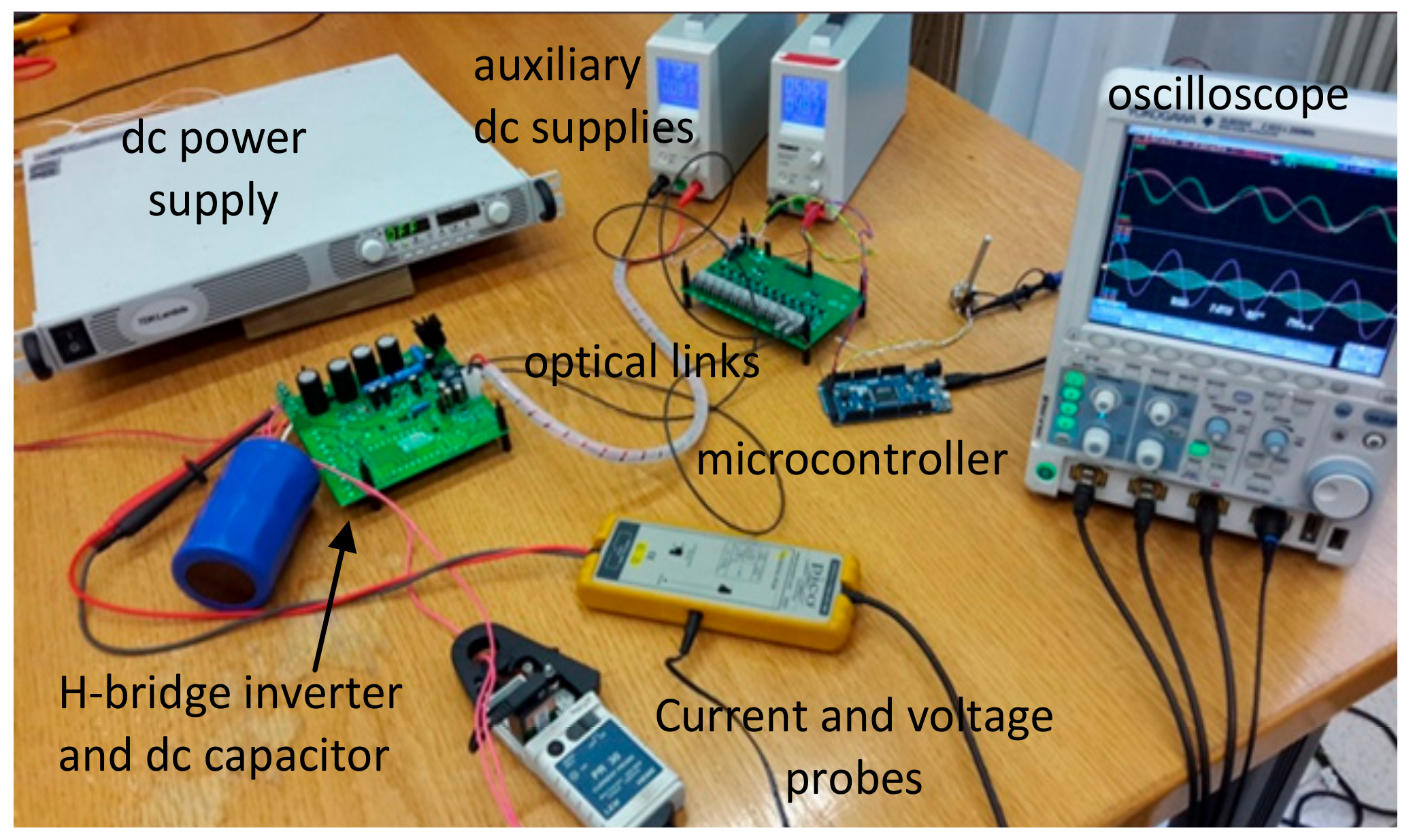
A picture of the whole lab setup is presented in Figure 10. It consists of a Mitsubishi power IGBT module IPM PS22A76 (1200 V, 25 A, Mitsubishi Electric Corporation, Tokyo, Japan), an “Arduino DUE” microcontroller board (84 MHz Atmel, SAM3X83 Cortex-M3 CPU, Somerville, MA, USA), and a Yokogawa DLM 2024 oscilloscope (Yokogawa Electric Corporation, Tokyo, Japan) with the PICO TA057 differential voltage probe (25 MHz, ±1400 V, ±2%, Pico Technology, Tyler, TX, USA) and LEM PR30 current probe (dc to 20 kHz, ±20 A, ±1%, LEM Europe GmbH, Fribourg, Switzerland). Additionally, not included in Figure 10, an air-core inductor (RL) is adopted as a DC-source impedance in series with the DC power supply.
In Figure 11 the electrical circuit scheme of the load is presented. The corresponding load parameters presented in Table 3 have been determined by the LCR meter Agilent 4263B.
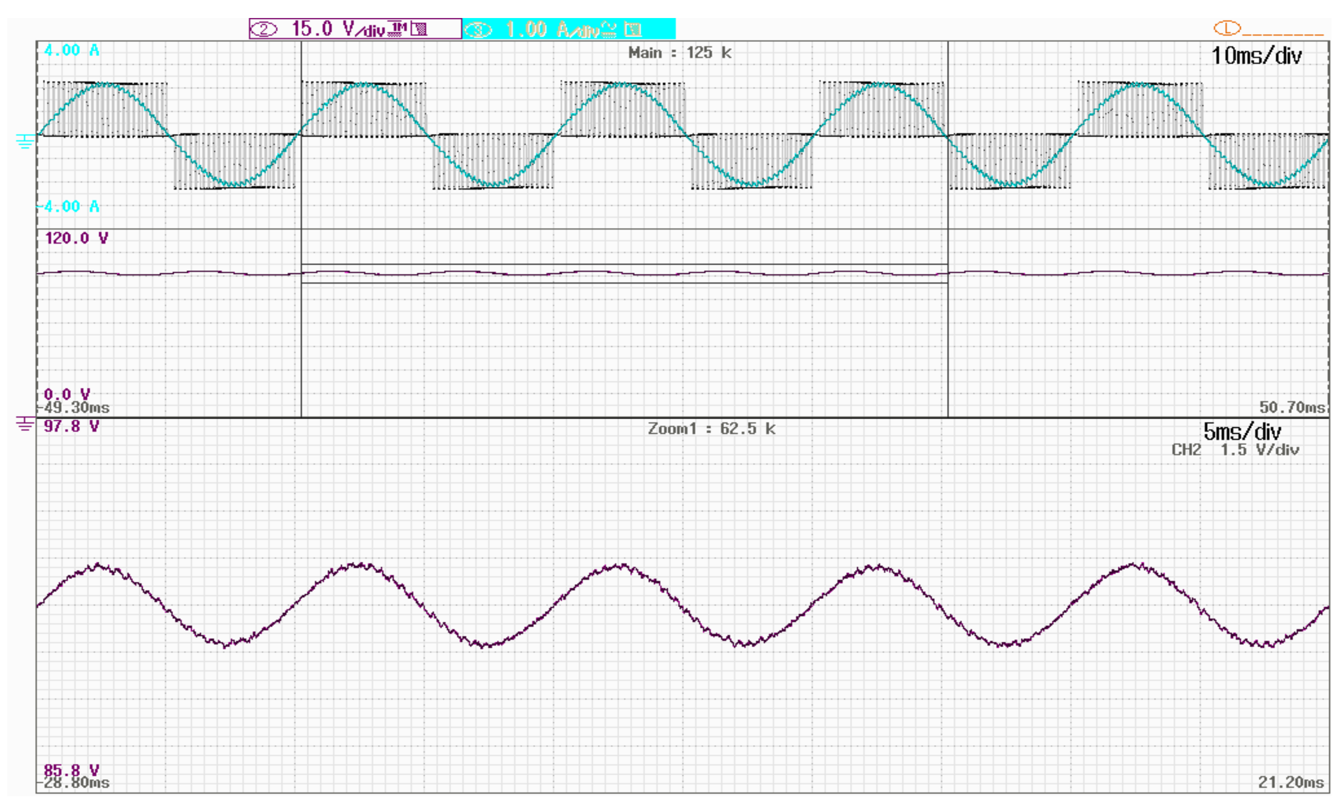
As a first experimental verification, the load voltage and current, and the DC-link voltage were measured. In Figure 12, the aforesaid variables are presented for the case m = 0.75 and ϕ = 0°, over five fundamental periods (5T = 100 ms). The top part of the oscilloscope screenshot presents the load voltage and current, the middle part presents the DC-link voltage, and the bottom part presents one zoomed part of the DC-link voltage emphasizing the presence of 100 Hz and switching ripple components. The zoomed part of the DC bus voltage is marked with the rectangle in the middle part of the screenshot, showing five periods of the 100 Hz components.
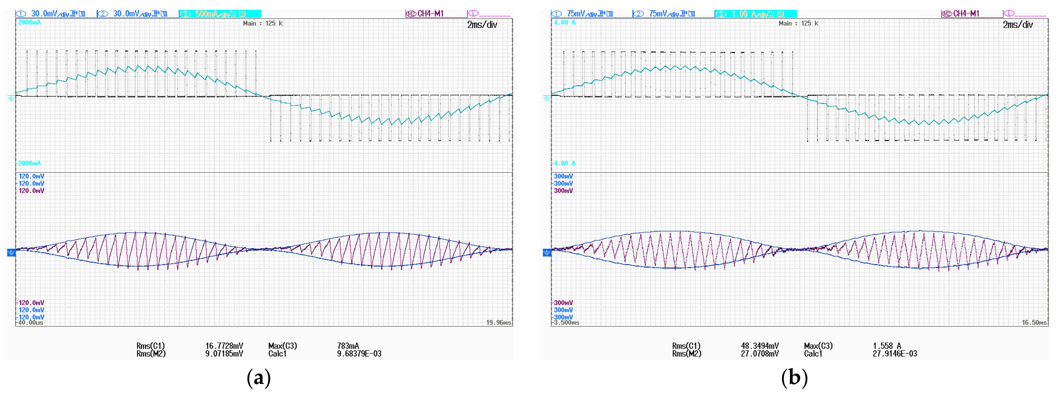
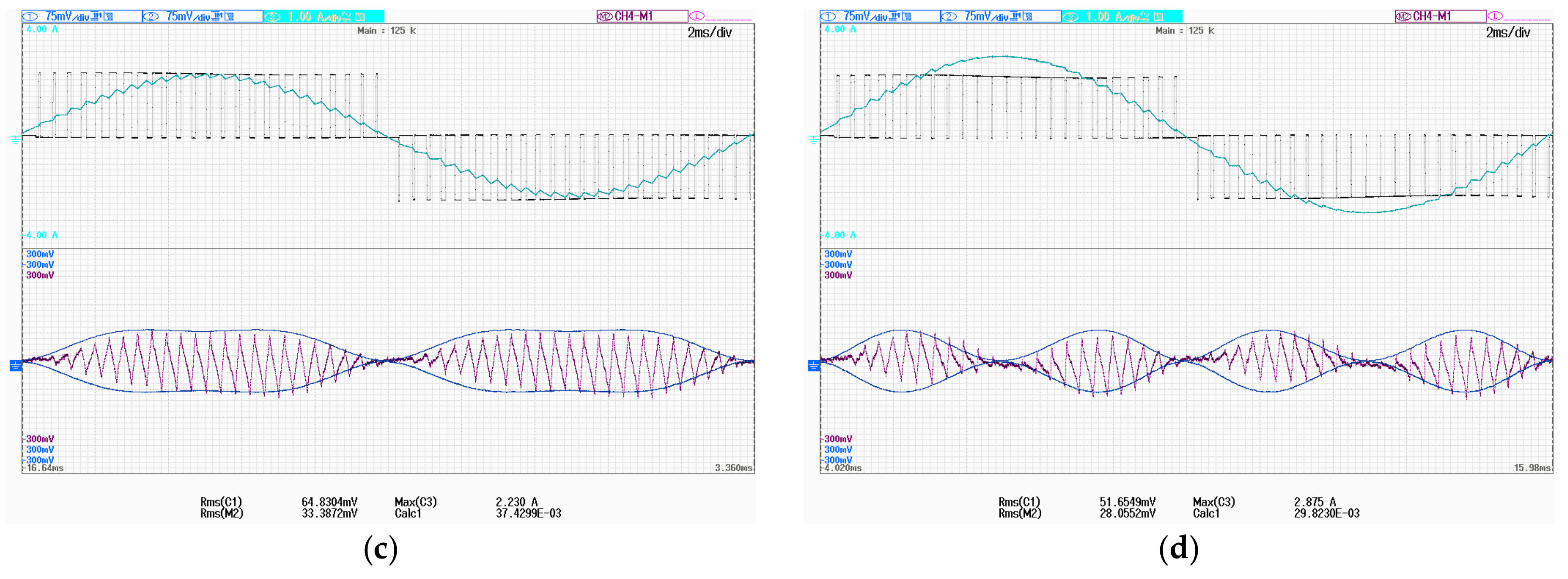
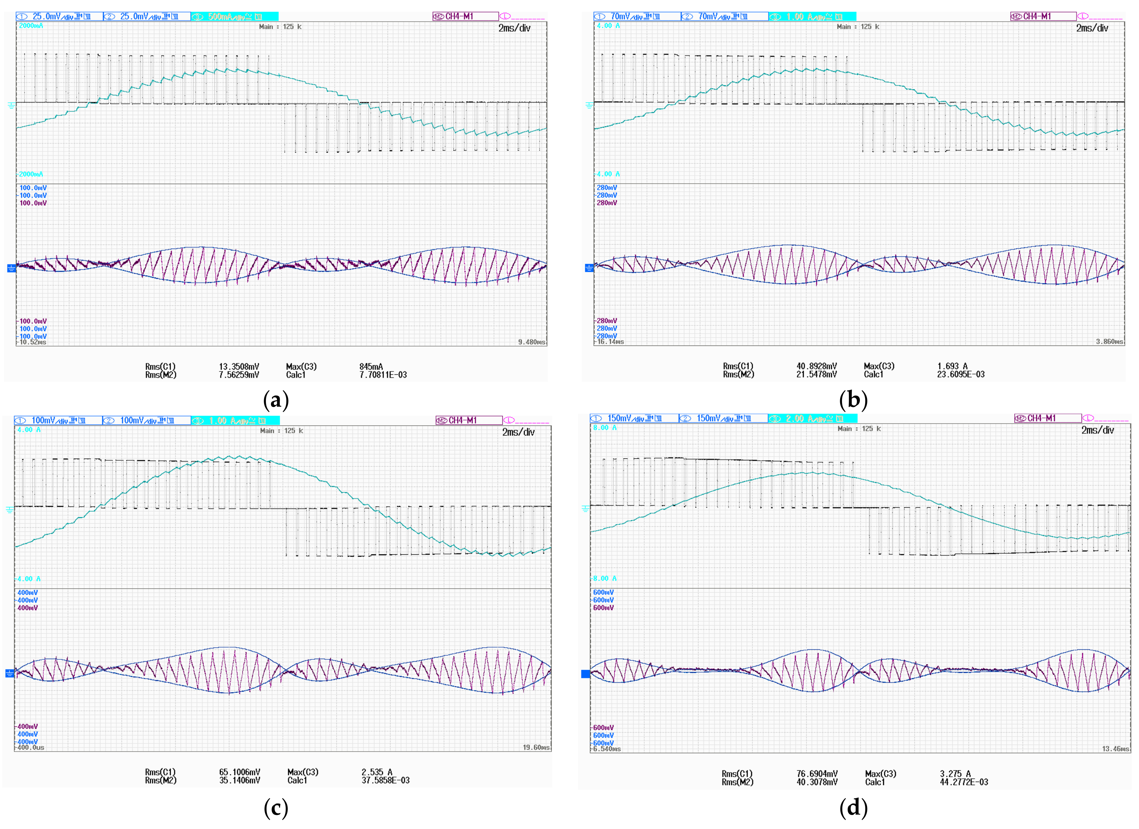
In Figure 13 and Figure 14, experimental verifications were carried out considering four different values of the modulation index m = 0.25, 0.5, 0.75, and 1, for the case of output phase angles ϕ = 0° and ϕ = 60°, respectively. In both figures, there are five traces displayed over one fundamental period: top traces present the load voltage and corresponding load current; a violet trace presents the DC-link voltage switching ripple. The two blue traces present the two half envelopes of the mentioned ripple (±∆vpp/2), obtained by implementing Equation (19) in the microcontroller board and sending to an output digital-to-analog converter (DAC) channel, with a proper scale factor.
Similarly to the simulations, the switching ripple component of the DC-link voltage has been obtained by filtering the instantaneous DC-voltage using the built-in math functions of the scope.
As it can be noticed, the experimental voltage ripples match the theoretical envelopes in a very satisfactory way for all the considered cases, both in the amplitude and the shape, confirming the effectiveness of the proposed analytical developments given by Equation (19).
The RMS of the envelope (Rms(C1)), maximum value of the output current (Max(C3)), RMS of the ripple (Rms(M2)), and RMS of the envelope divided by sqrt(3) (Calc1) are presented at the bottom of Figure 13 and Figure 14.
Table 4 summarizes the analytical, numerical, and experimental RMS values of the DC-link voltage switching ripple (ΔVrms) for the considered cases. The matching is generally satisfying within the expected resolution and considering the non-idealities of the experimental implementation.
7. Conclusions
An analysis, detailed calculations, and experimental verifications of the instantaneous DC-link voltage ripple in single-phase H-bridge PWM inverters have been carried out and presented in this paper, considering both the double-fundamental frequency component and the switching frequency component, and taking into account different types of DC source impedances.
In particular, the expression of the peak-to-peak voltage switching ripple amplitude was derived over the whole fundamental period as a function of the modulation index m and the output current phase angle ϕ. The normalized voltage switching ripple amplitude was introduced, and different diagrams were investigated. The maximum of the peak-to-peak amplitude and the RMS of the DC-link voltage switching ripple were determined, leading to simple and effective guidelines for designing a DC-link capacitor based on voltage ripple requirements.
The analytical developments have been experimentally verified using two different kinds of custom-made load, corresponding to ϕ = 0° (as for most of the grid-connected inverters) and ϕ = 60° (typical inductive load), and four modulation indexes to cover the whole modulation range. The RMS values of the switching ripple were calculated in real time using the advanced oscilloscope function and displayed together with the corresponding waveforms. For all considered cases, the theoretical and experimental results showed a satisfactory matching. All in all, the effectiveness and correctness of the developments have been successfully proven. The proposed methodology could be extended to different DC/AC conversion topologies, such as multilevel and multiphase inverters.
Author Contributions
All the authors gave their contribution to all of the aspects of the manuscript. To emphasize a particular specific contribution, Marija Vujacic composed the paper and together with Manel Hammami developed the analytical and simulation results. Milan Srndovic arranged the setup and performed the experimental tests, and Gabriele Grandi supervised all the work.
Conflicts of Interest
The authors declare no conflict of interest.
References
- Holmes, G.D.; Lipo, T.A. Pulse Width Modulation for Power Converters—Principles and Practice; IEEE Series on Power Engineering; John Wiley and Sons: Piscataway, NJ, USA, 2003. [Google Scholar]
- Hava, A.M.; Kerkman, R.J.; Lipo, T.A. Carrier-based PWM-VSI overmodulation strategies: Analysis, comparison, and design. IEEE Trans. Power Electron. 1998, 13, 674–689. [Google Scholar] [CrossRef]
- Zhao, D.; Hari, V.S.S.P.K.; Narayanan, G.; Ayyanar, R. Space-vector-based hybrid pulsewidth modulation techniques for reduces harmonic distorstion and switching loss. IEEE Trans. Power Electron. 2010, 25, 760–774. [Google Scholar] [CrossRef]
- Fuente, D.V.; Rodríguez, C.L.T.; Garcerá, G.; Figueres, E.; Gonzales, R.O. Photovoltaic power system with battery backup with grid-connection and islanded operation capabilities. IEEE Trans. Ind. Electron. 2013, 60, 1571–1581. [Google Scholar] [CrossRef]
- Serban, I. Power decoupling method for single-phase H-Bridge inverters with no additional power electronics. IEEE Trans. Ind. Electron. 2015, 62, 4805–4813. [Google Scholar] [CrossRef]
- Wai, R.J.; Lin, C.Y.; Huang, Y.C.; Chang, Y.R. Design of high-performance stand-alone and grid-connected inverter for distributed generation applications. IEEE Trans. Ind. Electron. 2013, 60, 1542–1555. [Google Scholar] [CrossRef]
- Grandi, G.; Loncarski, J. Evaluation of current ripple amplitude in three-phase PWM voltage source inverters. In Proceedings of the 8th IEEE Conference on Compatibility and Power Electronics (CPE), Ljubljana, Slovenia, 5–7 June 2013. [Google Scholar]
- Jiang, D.; Wang, F. Current-ripple prediction for three-phase PWM converters. IEEE Trans. Ind. Appl. 2014, 50, 531–538. [Google Scholar] [CrossRef]
- Grandi, G.; Loncarski, J.; Dordjevic, O. Analysis and comparison of peak-to-peak current ripple in two-level and multilevel PWM inverters. IEEE Trans. Ind. Electron. 2015, 62, 2721–2730. [Google Scholar] [CrossRef]
- Grandi, G.; Loncarski, J.; Rossi, C. Comparison of peak-to-peak current ripple amplitude in multiphase PWM voltage source inverters. In Proceedings of the 15th IEEE Conference on Power Electronics and Applications (EPE), Lille, France, 3–5 September 2013. [Google Scholar]
- Reznikov, B.; Srndovic, M.; Familiant, Y.L.; Grandi, G.; Ruderman, A. Simple time averaging current quality evaluation of a single-phase multilevel PWM inverter. IEEE Trans. Ind. Electron. 2016, 63, 3605–3615. [Google Scholar] [CrossRef]
- Wang, H.; Blaabjerg, F. Reliability of capacitors for DC-link applications in power electronic converters—An overview. IEEE Trans. Ind. Electron. 2014, 50, 3569–3578. [Google Scholar] [CrossRef]
- Arya, A.; Ahmad, M. W.; Agarwal, N.; Anand, S. Capacitor impedance estimation utilizing dc-link voltage oscillations in single phase inverter. IET Power Electron. 2017, 10, 1046–1053. [Google Scholar] [CrossRef]
- Kolar, J.W.; Round, S.D. Analytical calculation of the RMS current stress on the DC-link capacitor of voltage-PMW converter systems. IEE Proc. Electr. Power Appl. 2006, 153, 535–543. [Google Scholar] [CrossRef]
- Dahono, P.A.; Sato, Y.; Kataoka, T. Analysis and minimization of ripple components of input current and voltage of PWM inverters. IEEE Trans. Ind. Appl. 1996, 32, 945–950. [Google Scholar] [CrossRef]
- Gohil, G.; Bede, L.; Teodorescu, R.; Kerekes, T.; Blaabjerg, F. Analytical method to calculate the DC link current stress in voltage source converters. In Proceedings of the IEEE International Conference on Power Electronics, Drives and Energy Systems (PEDES), Mumbai, India, 16–19 December 2014. [Google Scholar]
- Wu, T.F.; Kuo, C.L.; Lin, L.C.; Chen, Y.K. DC-Bus voltage regulation for a DC distribution system with a single-phase bidirectional inverter. IEEE J. Emerg. Sel. Top. Power Electron. 2016, 4, 210–220. [Google Scholar] [CrossRef]
- Bierhoff, M.H.; Fuchs, F.W. DC-Link harmonics of three phase voltage-source converters influenced by the pulsewidth modulation strategy—An analysis. IEEE Trans. Ind. Electron. 2008, 55, 2085–2092. [Google Scholar] [CrossRef]
- McGrath, B.P.; Holmes, D.G. A general analytical method for calculating inverter DC-link current harmonics. IEEE Trans. Ind. Electron. 2009, 45, 1851–1859. [Google Scholar] [CrossRef]
- Renken, F. The DC-link capacitor current in pulsed single-phase H-bridge inverters. In Proceedings of the European Conference on Power Electronics, Dresden, Germany, 11–14 September 2005; pp. 1–10. [Google Scholar]
- Renken, F. Analytic calculation of the DC-link capacitor current for pulsed three-phase inverters. In Proceedings of the 11th International Conference on Power Electronics and Motion Control, Riga, Latvia, 2–4 September 2004. [Google Scholar]
- Pei, X.; Zhou, W.; Kang, Y. Analysis and calculation of DC-link current and voltage ripples for three-phase inverter with unbalanced load. IEEE Trans. Ind. Electron. 2015, 30, 5401–5412. [Google Scholar] [CrossRef]
- Vujacic, M.; Srndovic, M.; Hammami, M.; Grandi, G. Evaluation of DC voltage ripple in single-phase H-bridge PWM inverters. In Proceedings of the 42nd Conference of the IEEE Industrial Electronics Society, Florence, Italy, 24–27 October 2016. [Google Scholar]
Figure 1.
Basic circuit scheme of the single-phase full-bridge (H-bridge) inverter to determine the DC-link voltage ripple.
Figure 1.
Basic circuit scheme of the single-phase full-bridge (H-bridge) inverter to determine the DC-link voltage ripple.

Figure 2.
Ideal pulse-width modulation (PWM) inverter output voltage (instantaneous component, blue trace) and its averaged counterpart (fundamental component, red trace) in case of Vdc = 100 V and m = 1.
Figure 2.
Ideal pulse-width modulation (PWM) inverter output voltage (instantaneous component, blue trace) and its averaged counterpart (fundamental component, red trace) in case of Vdc = 100 V and m = 1.

Figure 3.
Ideal PWM inverter input current (green trace), its averaged counterpart (purple trace), and average component (dashed line) in case of m = 1, Io = 5 A (sinusoidal output current, 50 Hz), and ϕ = 60°.
Figure 3.
Ideal PWM inverter input current (green trace), its averaged counterpart (purple trace), and average component (dashed line) in case of m = 1, Io = 5 A (sinusoidal output current, 50 Hz), and ϕ = 60°.

Figure 4.
Instantaneous input current and DC-link voltage over a switching period Ts.

Figure 5.
Normalized peak-to-peak DC-link voltage ripple amplitude rpp(ϑ) in a half-fundamental period (0, 180°) for different modulation indices, m = 0.25, 0.5, 0.75, and 1, and output phase angle (a) ϕ = 0°; (b) ϕ = 30°; (c) ϕ = 60°, and (d) ϕ = 90°.
Figure 5.
Normalized peak-to-peak DC-link voltage ripple amplitude rpp(ϑ) in a half-fundamental period (0, 180°) for different modulation indices, m = 0.25, 0.5, 0.75, and 1, and output phase angle (a) ϕ = 0°; (b) ϕ = 30°; (c) ϕ = 60°, and (d) ϕ = 90°.

Figure 6.
Maximum of normalized peak-to-peak voltage switching ripple amplitude vs. modulation index for different output phase angles ϕ = 0°, 30°, 60°, and 90°.
Figure 6.
Maximum of normalized peak-to-peak voltage switching ripple amplitude vs. modulation index for different output phase angles ϕ = 0°, 30°, 60°, and 90°.

Figure 7.
Root-mean-square (RMS) of normalized voltage switching ripple vs. modulation index for different output phase angles ϕ = 0°, 30°, 60°, and 90°.
Figure 7.
Root-mean-square (RMS) of normalized voltage switching ripple vs. modulation index for different output phase angles ϕ = 0°, 30°, 60°, and 90°.

Figure 8.
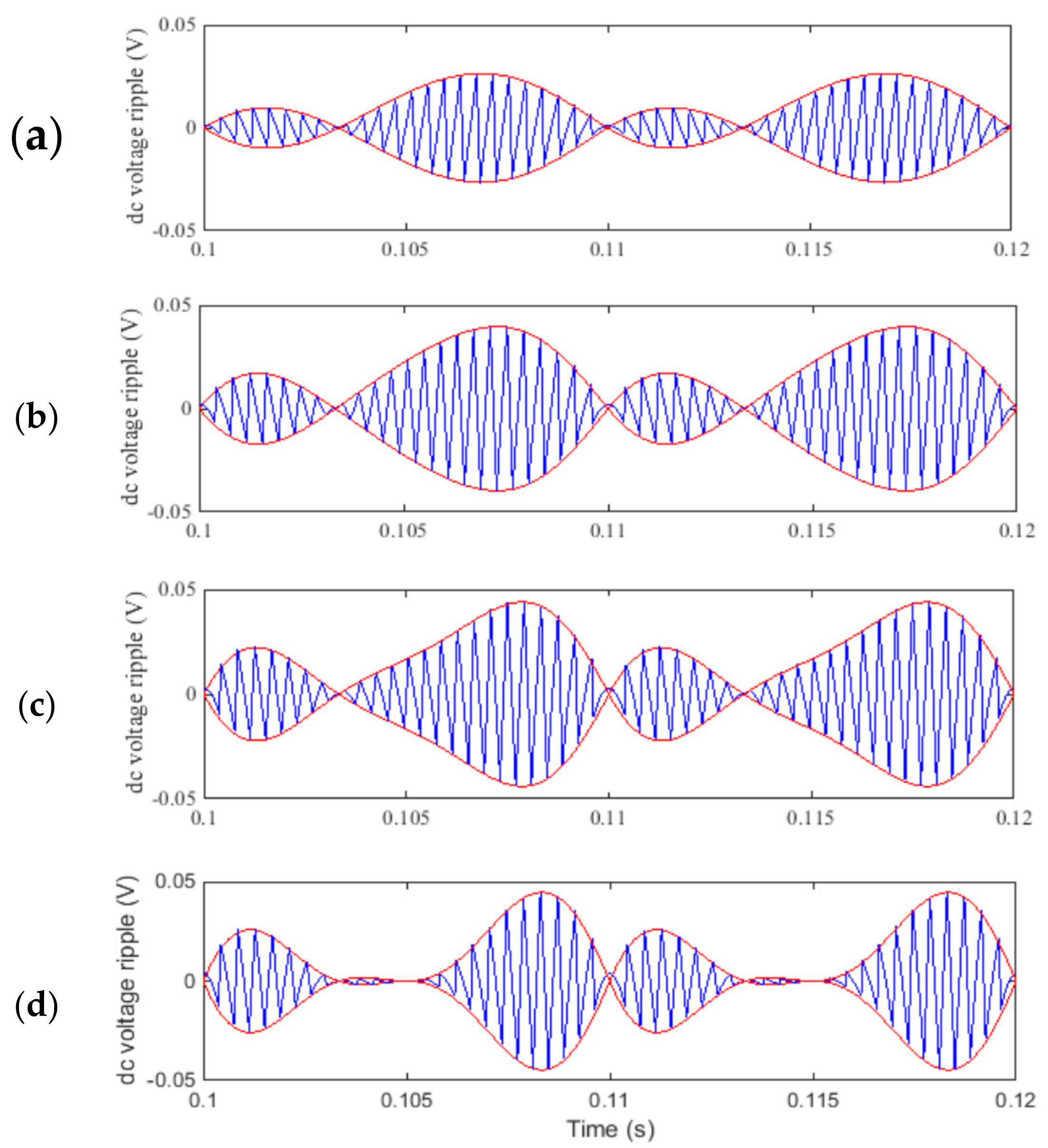
DC-link voltage switching ripple: simulation results (blue trace) and theoretical peak-to-peak envelope (red trace) over a fundamental period for ϕ = 0°, (a) m = 0.25; (b) m = 0.5; (c) m = 0.75; and (d) m = 1.
Figure 8.
DC-link voltage switching ripple: simulation results (blue trace) and theoretical peak-to-peak envelope (red trace) over a fundamental period for ϕ = 0°, (a) m = 0.25; (b) m = 0.5; (c) m = 0.75; and (d) m = 1.


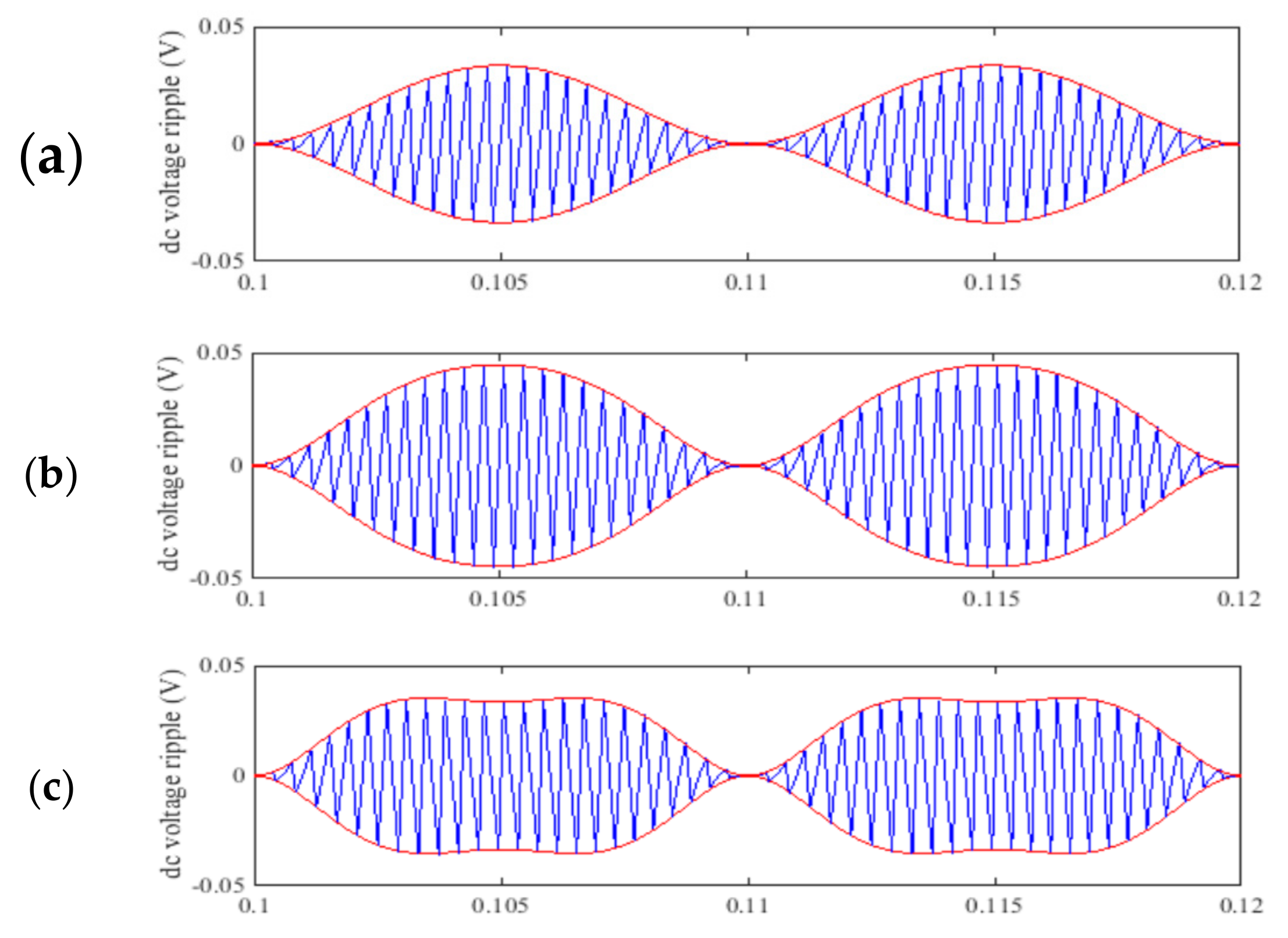
Figure 9.
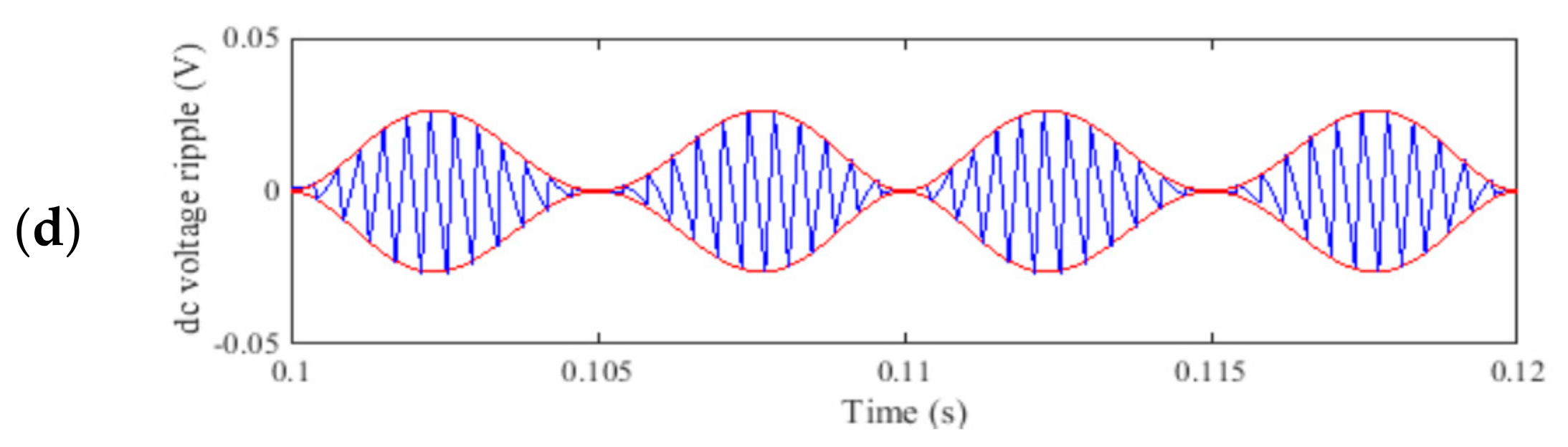
DC-link voltage switching ripple: simulation results (blue trace) and theoretical peak-to-peak envelope (red trace) over a fundamental period for ϕ = 60°, (a) m = 0.25; (b) m = 0.5; (c) m = 0.75; and (d) m = 1.
Figure 9.
DC-link voltage switching ripple: simulation results (blue trace) and theoretical peak-to-peak envelope (red trace) over a fundamental period for ϕ = 60°, (a) m = 0.25; (b) m = 0.5; (c) m = 0.75; and (d) m = 1.

Figure 10.
Experimental setup.

Figure 11.
Load configuration for the experimental setup.

Figure 12.
Output load voltage and current: upper part, dc-link voltage: middle part, and zoomed DC-link ripple components: lower part, for m = 0.75 and ϕ = 0°.
Figure 12.
Output load voltage and current: upper part, dc-link voltage: middle part, and zoomed DC-link ripple components: lower part, for m = 0.75 and ϕ = 0°.

Figure 13.
Experimental results for ϕ = 0°: upper half, output voltage and current; lower half, analytically calculated envelope and measured DC voltage switching ripple. (a) m = 0.25; (b) m = 0.50; (c) m = 0.75; (d) m = 1.
Figure 13.
Experimental results for ϕ = 0°: upper half, output voltage and current; lower half, analytically calculated envelope and measured DC voltage switching ripple. (a) m = 0.25; (b) m = 0.50; (c) m = 0.75; (d) m = 1.


Figure 14.
Experimental results for ϕ = 60°: upper half, output voltage and current; lower half, analytically calculated envelope and measured DC voltage switching ripple. (a) m = 0.25; (b) m = 0.50; (c) m = 0.75; (d) m = 1.
Figure 14.
Experimental results for ϕ = 60°: upper half, output voltage and current; lower half, analytically calculated envelope and measured DC voltage switching ripple. (a) m = 0.25; (b) m = 0.50; (c) m = 0.75; (d) m = 1.


Table 1.
Circuit parameters.
| Label | Description | Parameters |
|---|---|---|
| Vdc | DC voltage supply | 96 V |
| R | DC source resistance | 5.4 Ω |
| L | DC source inductance | 19 mH |
| C | DC-link capacitance | 1.1 mF |
| fS | Switching frequency | 2.5 kHz |
| Io | Sinusoidal output current amplitude | 1 A |
| f | Fundamental frequency | 50 Hz |
Table 2.
Experimental setup parameters.
| Label | Description | Parameters |
|---|---|---|
| Vdc | DC voltage supply | 96 V |
| R | DC source resistance | 5.5 Ω |
| L | DC source inductance | 19 mH |
| C | DC-link capacitance | 1.1 mF |
| fS | Switching frequency | 2.5 kHz |
| f | Fundamental frequency | 50 Hz |
Table 3.
Load parameters.
| Load | ϕ = 0° | ϕ = 60° |
|---|---|---|
| RL | 4.7 Ω | 13.9 Ω |
| LL | 43.3 mH | 76.4 mH |
| Ro | 29.7 Ω | 0 |
| Co | 43.3 μF | 0 |
Table 4.
Summarizes the analytical (Theory), numerical (Sim.), and experimental (Exp.) RMS values of the DC-link.
Table 4.
Summarizes the analytical (Theory), numerical (Sim.), and experimental (Exp.) RMS values of the DC-link.
| m | Load Angle ϕ = 0° | Load Angle ϕ = 60° | ||||
|---|---|---|---|---|---|---|
| Theory | Sim. | Exp. | Theory | Sim. | Exp. | |
| 0.25 | 9.7 | 9.6 | 9.1 | 7.8 | 7.8 | 7.7 |
| 0.5 | 27.5 | 26.8 | 27.1 | 23.6 | 23.6 | 21.6 |
| 0.75 | 37.4 | 35.6 | 33.4 | 37.5 | 37.5 | 35.1 |
| 1.00 | 29.9 | 28.7 | 28.1 | 44.23 | 44.3 | 40.3 |
© 2017 by the authors. Licensee MDPI, Basel, Switzerland. This article is an open access article distributed under the terms and conditions of the Creative Commons Attribution (CC BY) license (http://creativecommons.org/licenses/by/4.0/).
Share and Cite
MDPI and ACS Style
Vujacic, M.; Hammami, M.; Srndovic, M.; Grandi, G. Theoretical and Experimental Investigation of Switching Ripple in the DC-Link Voltage of Single-Phase H-Bridge PWM Inverters. Energies 2017, 10, 1189. https://doi.org/10.3390/en10081189
AMA Style
Vujacic M, Hammami M, Srndovic M, Grandi G. Theoretical and Experimental Investigation of Switching Ripple in the DC-Link Voltage of Single-Phase H-Bridge PWM Inverters. Energies. 2017; 10(8):1189. https://doi.org/10.3390/en10081189
Chicago/Turabian StyleVujacic, Marija, Manel Hammami, Milan Srndovic, and Gabriele Grandi. 2017. "Theoretical and Experimental Investigation of Switching Ripple in the DC-Link Voltage of Single-Phase H-Bridge PWM Inverters" Energies 10, no. 8: 1189. https://doi.org/10.3390/en10081189
Note that from the first issue of 2016, this journal uses article numbers instead of page numbers. See further details here.