Bidirectional Interleaved PWM Converter with High Voltage-Conversion Ratio and Automatic Current Balancing Capability for Single-Cell Battery Power System in Small Scientific Satellites


Abstract
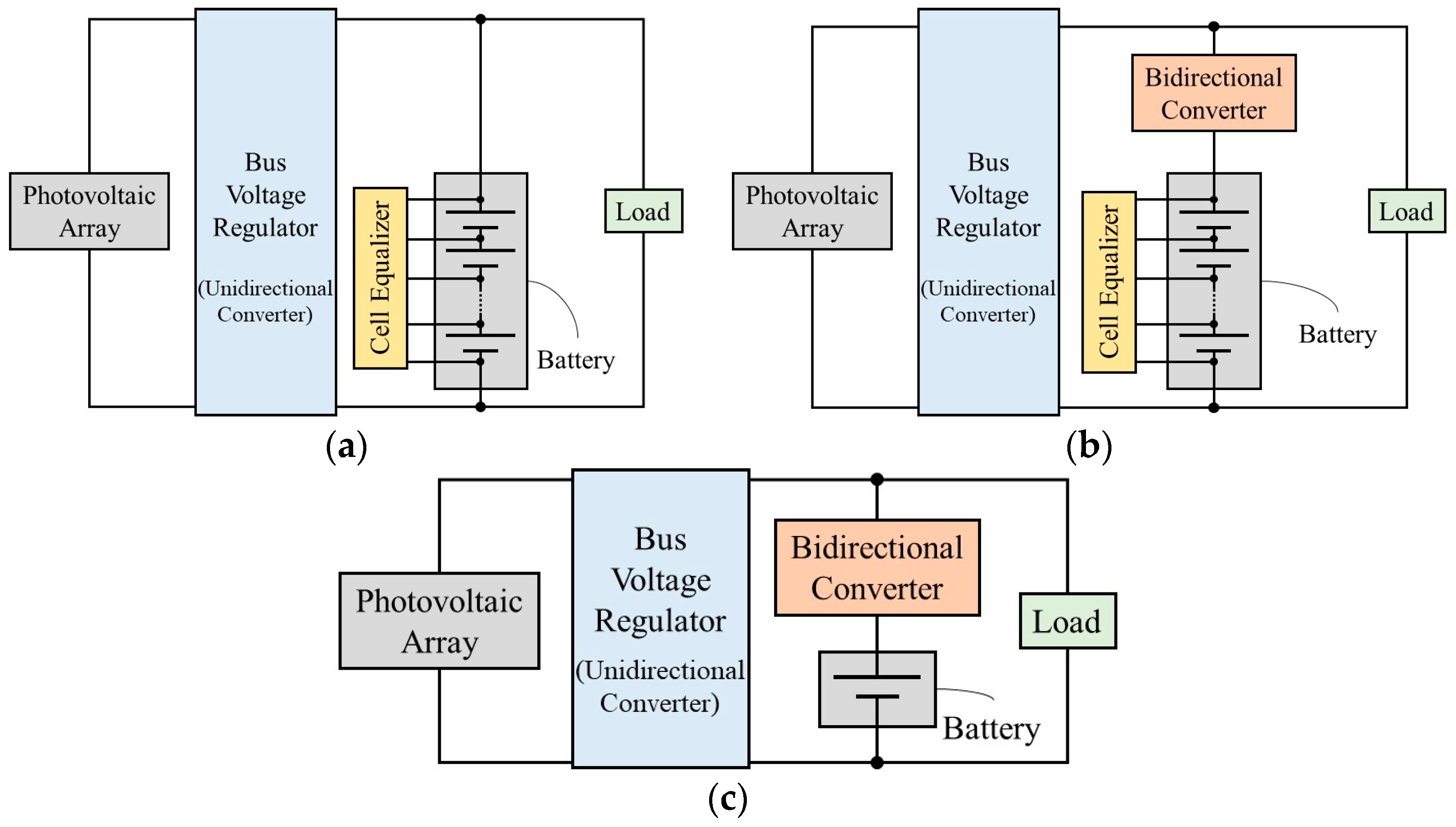
:1. Introduction
2. Interleaved Bidirectional PWM Converter with High Voltage-Conversion Ratio and Automatic Current Balancing Capability
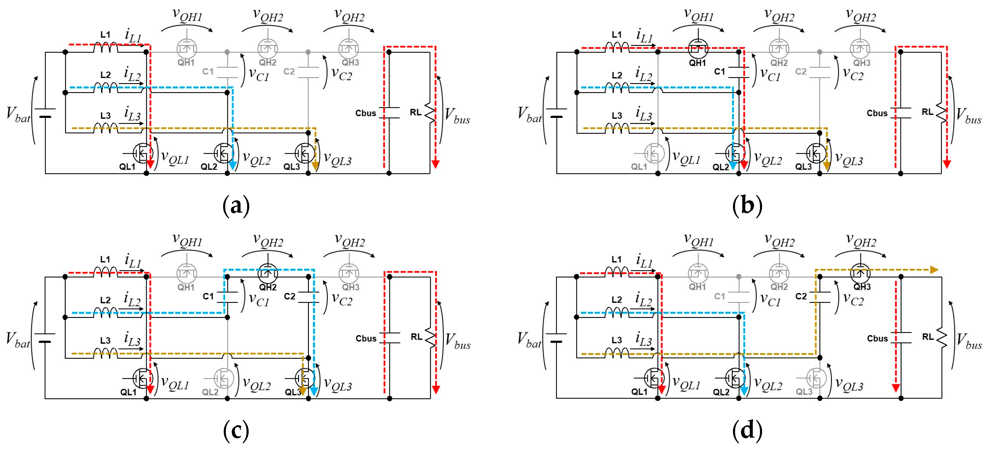
3. Operation Analysis
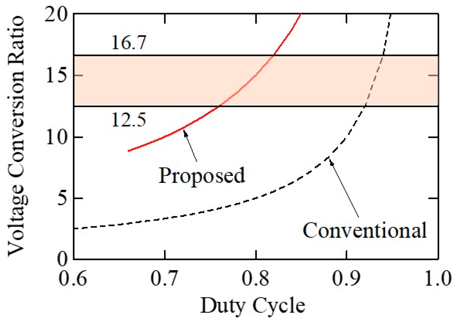
3.1. Operation Modes and Voltage Conversion Ratio
3.2. Current Balancing Mechanism
4. Quantitative Comparison
4.1. Total Device Power Rating
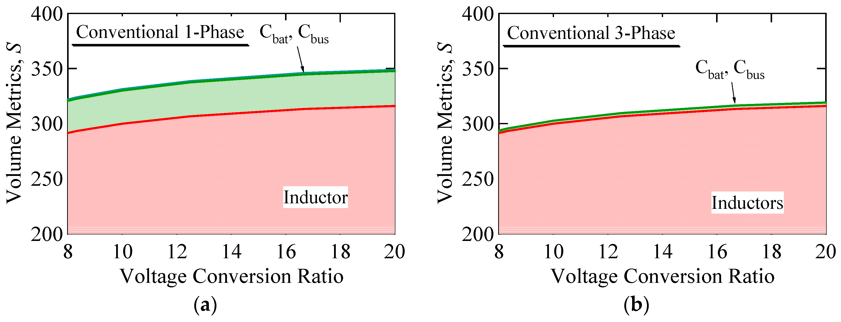
4.2. Normalized Charged-Discharged Energies in Passive Components
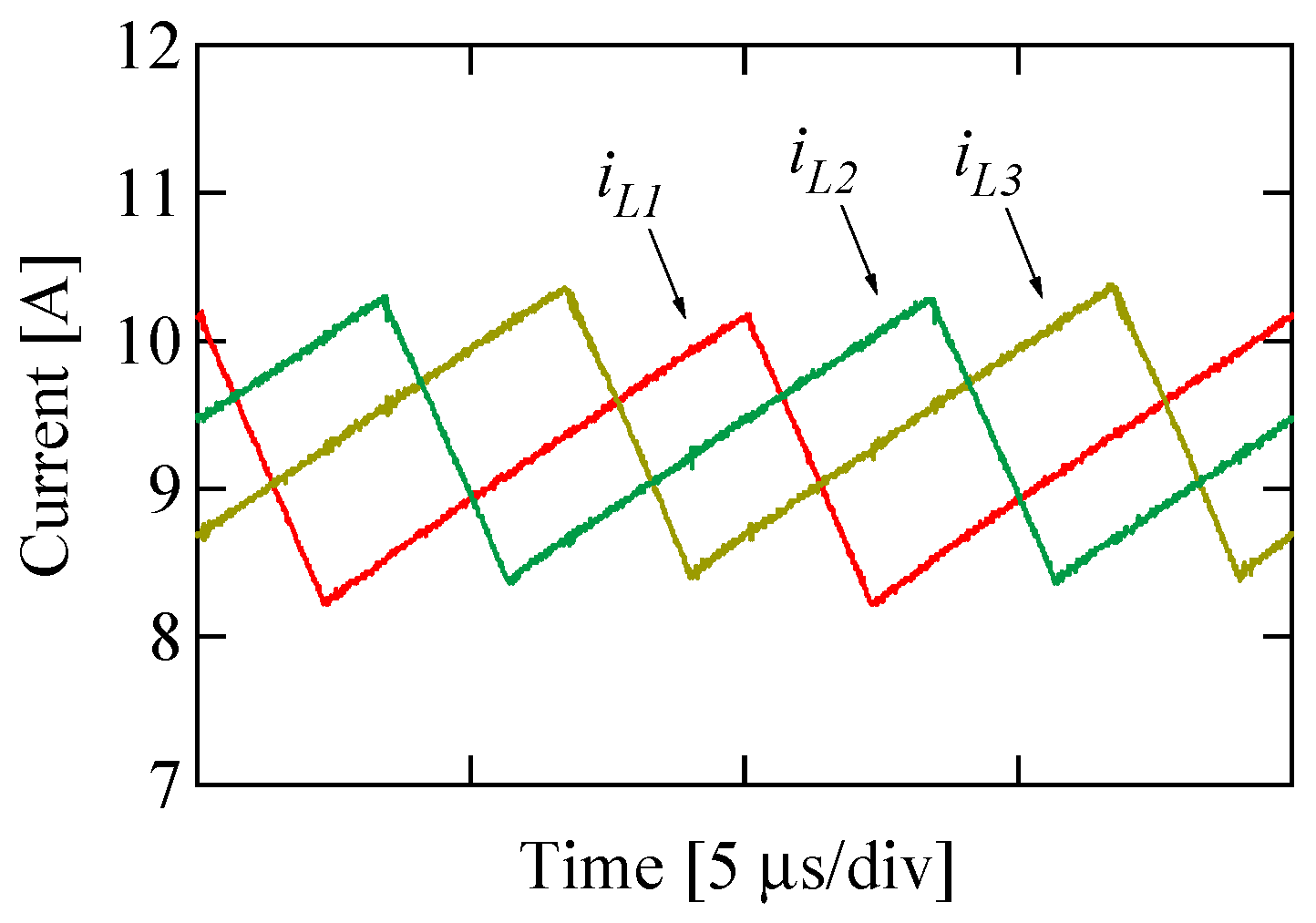
5. Experimental Results
6. Conclusions
Author Contributions
Funding
Conflicts of Interest
Nomenclature
| αC, αL | Ripple factor of capacitor voltage and inductor current |
| β | Energy density ratio of capacitors to inductors |
| d1, d2, d3 | Duty cycle of QL1, QL2, QL3 |
| EC, EL | Charged-discharged energy of capacitors and inductors |
| Ibus (A) | Average bus current |
| IL (A) | Balanced average inductor current |
| iL1, iL2, iL3 (A) | Instantaneous inductor current of L1, L2, L3 |
| IL1, IL2, IL3 (A) | Average inductor current of L1, L2, L3 |
| Imax (A) | Theoretical maximum current stress of MOSFETs |
| q1, q2, q3 (C) | Amount of charge released by iL1, iL2, iL3 |
| S | Size metrics |
| Ts [s] | Switching period |
| TDPR | Total device power rating |
| VC1, VC2 (V) | Voltage of C1, C2 |
| Vbat (V) | Battery voltage |
| VCbus (V) | Bus voltage |
| Vmax (V) | Theoretical maximum voltage stress of MOSFETs |
References
- Uno, M.; Kukita, A. Multi-port converter integrating boost and switched capacitor converters for single-cell battery power system in small satellite. In Proceedings of the IEEE ECCE-Asia Down Under, Melbourne, Australia, 3–6 June 2013; pp. 747–752. [Google Scholar]
- Cassani, P.A.; Williamson, S.S. Design, testing, and validation of a simplified control scheme for a novel plug-ion hybrid electric vehicle battery cell equalizer. IEEE Trans. Ind. Electron. 2010, 57, 3956–3962. [Google Scholar] [CrossRef]
- Baughman, A.; Ferdowsi, M. Double-tiered switched-capacitor battery charge equalization technique. IEEE Trans. Ind. Appl. 2008, 55, 2277–2285. [Google Scholar] [CrossRef]
- Uno, M.; Tanaka, K. Influence of high-frequency charge-discharge cycling induced by cell voltage equalizers on the life performance of lithium-ion cells. IEEE Trans. Veh. Technol. 2011, 60, 1505–1515. [Google Scholar] [CrossRef]
- Shang, Y.; Zhang, Q.; Cui, N.; Zhang, C. A cell-to-cell equalizer based on three-resonant-state switched-capacitor converters for series-connected battery strings. Energies 2017, 10, 206. [Google Scholar] [CrossRef]
- Uno, M.; Kukita, A. Double-switch equalizer using parallel- or series-parallel-resonant inverter and voltage multiplier for series-connected supercapacitors. IEEE Trans. Power Electron. 2014, 29, 812–828. [Google Scholar] [CrossRef]
- Arias, M.; Sebastian, J.; Hernando, M.M.; Viscarret, U.; Gil, I. Practical application of the wave-trap concept in battery–cell equalizers. IEEE Trans. Power Electron. 2015, 30, 5616–5631. [Google Scholar] [CrossRef]
- Uno, M.; Kukita, A. Single-switch single-transformer cell voltage equalizer based on forward-flyback resonant inverter and voltage multiplier for series-connected energy storage cells. IEEE Trans. Veh. Technol. 2014, 63, 4232–4247. [Google Scholar] [CrossRef]
- Li, L.; Huang, Z.; Li, H.; Lu, H. A high-efficiency voltage equalization scheme for supercapacitor energy storage system in renewable generation applications. Sustainability 2016, 8, 548. [Google Scholar] [CrossRef]
- Bui, T.M.; Kim, C.H.; Kim, K.H.; Rhee, S.B. A modular cell balancer based on multi-winding transformer and switched-capacitor circuits for a series-connected battery string in electric vehicles. Appl. Sci. 2018, 8, 1278. [Google Scholar] [CrossRef]
- Yao, K.; Ye, M.; Xu, M.; Lee, F.C. Tapped-inductor buck converter for high-step-down dc–dc conversion. IEEE Trans. Power Electron. 2015, 20, 775–780. [Google Scholar] [CrossRef]
- Hu, Y.; Xie, Y.; Fu, D.; Cheng, L. A new single-phase Π-type 5-level inverter using 3-yerminal switch-network. IEEE Trans. Ind. Electron. 2016, 63, 7165–7174. [Google Scholar] [CrossRef]
- Andrade, A.M.S.S.; Mattos, E.; Schuch, L.; Hey, H.L.; Martins, M.L.S. Synthesis and comparative analysis of very high step-up DC–DC converters adopting coupled-inductor and voltage multiplier cells. IEEE Trans. Power Electron. 2018, 33, 5880–5897. [Google Scholar] [CrossRef]
- Forouzesh, M.; Shen, Y.; Yari, K.; Siwakoti, Y.P.; Blaabjerg, F. High-efficiency high step-up DC–DC converter with dual coupled inductors for grid-connected photovoltaic systems. IEEE Trans. Power Electron. 2018, 33, 5967–5982. [Google Scholar] [CrossRef]
- Saeedian, M.; Adabi, M.E.; Hosseini, S.M.; Adabi, J.; Pouresmaeil, E. A novel step-up single source multilevel inverter: Topology, operating principle and modulation. IEEE Trans. Power Electron. 2018. [Google Scholar] [CrossRef]
- Uno, M.; Kukita, A. PWM switched capacitor converter with switched-capacitor-inductor cell for adjustable high step-down voltage conversion. IEEE Trans. Power Electron. 2018. [Google Scholar] [CrossRef]
- Zhang, Y.; Gao, Y.; Li, J.; Sumner, M. Interleaved switched-capacitor bidirectional DC-DC converter with wide voltage-gain range for energy storage systems. IEEE Trans. Power Electron. 2018, 33, 3852–3869. [Google Scholar] [CrossRef]
- Chen, H.C.; Lu, C.Y.; Rout, U.S. Decoupled master-slave current balancing control for three-phase interleaved boost converters. IEEE Trans. Power Electron. 2018, 33, 3683–3687. [Google Scholar] [CrossRef]
- Mao, H.; Yao, L.; Wang, C.; Batarseh, I. Analysis of inductor current sharing in nonisolated and isolated multiphase dc-dc converters. IEEE Trans. Ind. Electron. 2007, 54, 3379–3388. [Google Scholar] [CrossRef]
- Qian, W.; Cao, D.; Rivera, J.G.C.; Gebben, M.; Wey, D.; Peng, F.Z. A switched-capacitor dc-dc converter with high voltage gain and reduced component rating and count. IEEE Trans. Ind. Appl. 2012, 48, 1397–1406. [Google Scholar] [CrossRef]
- He, L. High-performance bridge modular switched-capacitor converter with small component requirement based on output impedance analysis for low loss. IEEE Trans. Power Electron. 2013, 28, 4668–4680. [Google Scholar] [CrossRef]
- Pasternak, S.R.; Kiani, M.H.; Rentmeister, J.S.; Stauth, J.T. Modeling and performance limits of switched-capacitor DC–DC converters capable of resonant operation with a single inductor. IEEE J. Emerg. Sel. Top. 2017, 5, 1746–1760. [Google Scholar] [CrossRef]
- Sanders, S.R.; Alon, E.; Le, H.P.; Seeman, M.D.; Jhon, M.; Ng, V.W. The road to fully integrated dc–dc conversion via the switched-capacitor approach. IEEE Trans. Power Electron. 2018, 28, 4146–4155. [Google Scholar] [CrossRef]
- Piqué, G.V.; Bergveld, H.J.; Alarcón, E. Survery and benchmark of fully integrated switching power converters: Switched-capacitor versus inductive approach. IEEE Trans. Power Electron. 2013, 28, 4156–4167. [Google Scholar] [CrossRef]
- Uno, M.; Sugiyama, K. Switched capacitor converter-based multi-port converter integrating bidirectional PWM and series-resonant converters for standalone photovoltaic systems. IEEE Trans. Power Electron. 2018. [Google Scholar] [CrossRef]


| Component | Voltage | Current |
|---|---|---|
| QL1 | Vbat/(1 − d) | IL |
| QH1 | 2Vbat/(1 − d) | IL |
| QL2 | Vbat/(1 − d) | 2IL |
| QH2 | 2Vbat/(1 − d) | IL |
| QL3 | Vbat/(1 − d) | 2IL |
| QH3 | Vbat/(1 − d) | IL |
| Component | Charged-Discharged Energy |
|---|---|
| L1–L3 | VbatILdTs |
| C1 | VbatILTs |
| C2 | 2VbatILTs |
| Cbus | 3VbatILd(1 − d)Ts |
| Cbat | αILVbat(3d − 2)Ts/24d |
| Component | Value |
|---|---|
| L1–L3 | 15 μH, 16.9 mΩ |
| Cbat | Ceramic Capacitor, 220 μF, 3.1 mΩ |
| Cbus | Al Electrolytic Capacitor, 272 μF, 5.0 mΩ |
| C1, C2 | Ceramic Capacitor, 22 μF, 6.0 mΩ |
| QL1–QL3, QH1–QH3 | N-Channel MOSFET, TPCA8050-H, Ron = 14.2 mΩ |
© 2018 by the authors. Licensee MDPI, Basel, Switzerland. This article is an open access article distributed under the terms and conditions of the Creative Commons Attribution (CC BY) license (http://creativecommons.org/licenses/by/4.0/).
Share and Cite
Uno, M.; Inoue, M.; Sato, Y.; Nagata, H. Bidirectional Interleaved PWM Converter with High Voltage-Conversion Ratio and Automatic Current Balancing Capability for Single-Cell Battery Power System in Small Scientific Satellites. Energies 2018, 11, 2702. https://doi.org/10.3390/en11102702
Uno M, Inoue M, Sato Y, Nagata H. Bidirectional Interleaved PWM Converter with High Voltage-Conversion Ratio and Automatic Current Balancing Capability for Single-Cell Battery Power System in Small Scientific Satellites. Energies. 2018; 11(10):2702. https://doi.org/10.3390/en11102702
Chicago/Turabian StyleUno, Masatoshi, Masahiko Inoue, Yusuke Sato, and Hikaru Nagata. 2018. "Bidirectional Interleaved PWM Converter with High Voltage-Conversion Ratio and Automatic Current Balancing Capability for Single-Cell Battery Power System in Small Scientific Satellites" Energies 11, no. 10: 2702. https://doi.org/10.3390/en11102702