Article

Capacitors Voltage Switching Ripple in Three-Phase Three-Level Neutral Point Clamped Inverters with Self-Balancing Carrier-Based Modulation

Department of Electrical, Electronic, and Information Engineering, University of Bologna, 40136 Bologna, Italy
*
Author to whom correspondence should be addressed.
Energies 2018, 11(12), 3244; https://doi.org/10.3390/en11123244
Submission received: 23 October 2018 / Revised: 13 November 2018 / Accepted: 19 November 2018 / Published: 22 November 2018

Abstract

:
This paper provides a comprehensive analysis of the capacitors voltage switching ripple for three-phase three-level neutral point clamped (NPC) inverter topologies. The voltage ripple amplitudes of the two dc-link capacitors are theoretically estimated as a function of both amplitude and phase angle of output current and the inverter modulation index. In particular, peak-to-peak distribution and maximum amplitudes of the capacitor voltage switching ripple over the fundamental period are obtained. A comparison is made considering different carrier-based pulse-width modulations in the case of almost all sinusoidal load currents, representing either grid connection or passive load with a negligible current ripple. Based on the voltage switching ripple requirements of capacitors, a simple and effective original equation for a preliminary sizing of the capacitors has been proposed. Numerical simulations and experimental tests have been carried out in order to verify the analytical developments.

1. Introduction

In industrial applications, the most used switching inverter is the two-level converter. Due to mass production, it is a relatively cheap and reliable configuration. Furthermore, as the number of semiconductor devices is low, they can be simply controlled by different types of pulse-width modulation (PWM) techniques. However, the main drawback of the two-level converter is the high harmonic content of the output voltage, which makes the use of bulky output filter necessary, increasing the cost of the system and the losses. The harmonic content can be reduced simply by increasing the PWM switching frequency, which leads to an increase of the switching losses. The use of power filters and high switching frequency has to be balanced to achieve reasonable converter costs with acceptable efficiency.
During the last decades, the drawbacks of the two-level converter motivated researchers to develop new converter topologies. A very promising inverter family, called multilevel inverters (MLIs), offer better quality output voltage waveforms with a reduced harmonic content comparing to the conventional two-level inverter topologies, increase the overall voltage and power rating of the converter, and generally mitigate the electromagnetic interferences.
The penetration of multilevel inverters has been steadily increasing due to their widespread usage in manufacturing, transport, energy, high-power drives and other industry applications. Several MLI topologies have been introduced and extensively studied in the literature. Most currently used multilevel topologies can be grouped: cascaded H-bridge (CHB), neutral point clamped (NPC), and flying capacitors (FC).
Multilevel inverters were initiated by the invention of the so-called NPC inverter in 1981 by Nabae et al. [1]. The NPC inverter uses a single DC bus subdivided into a number of voltage levels by a series string of capacitors. The voltages across the individual switches are clamped by diodes at the voltage level of only one capacitor of the series DC-link string. The major difficulty associated with control of the diode-clamped inverter is the balancing of the capacitor voltages [2,3]. To achieve that, many modulation techniques have been developed [4,5,6,7,8]. In particular, carrier-based modulation and space vector modulation (SVM) strategies, similar to those employed for conventional two-level three-phase inverters, can be readily modified and extended to fulfill the multilevel NPC requirements.
An essential part of MLI design is the selection of DC-link capacitors. The capacitors are a sensitive element of the inverter and a common source of failures. So far, regarding two-level converter systems, some papers have investigated the minimum DC-link capacitance and proposed methods for its size reduction [9,10]. Recently, based on the DC-link voltage analysis and considering both low- and/or high-frequency DC voltage components, simple and effective guidelines for designing the DC-link capacitor have been presented in [11] for single-phase H-bridge inverter, and in [12] for three-phase three-level flying capacitor inverter. Methods used to derive expressions for RMS value and harmonic spectrum of the capacitor current in two-level inverters, are extended to the three-level inverters in [13]. An analytical expression for calculating RMS current through the DC-link capacitor in a three-level NPC inverter is given in [14]. The analysis of the DC-link capacitor current in three-level NPC and CHB inverters and a new numerical approach for calculating the RMS value of the capacitor current is proposed in [15].
Evaluation of the low-frequency neutral-point voltage oscillations in the three-level NPC inverter using space vector modulation (SVM) techniques has been analyzed in [16]. A novel modulation strategy for the NPC inverter is proposed in [17] to overcome one of the main problems of this converter, which is the low-frequency voltage oscillation that appears in the neutral point. The proposed modulation strategy can completely remove this oscillation for all the operating conditions and for any kind of loads, even unbalanced and nonlinear loads.
Nowadays, NPC inverters are the most widely used three-level inverter topologies in the industrial applications, considering both the conventional and the T-type configurations (Figure 1). In order to choose the most suitable topology and hereby increase power efficiency, the comparison between of conventional NPC and T-type inverters has been investigated and reported in the literature [18], also considering the loss evaluation. An efficiency comparison of both over-mentioned topologies is presented in [19] and the result shows that the T-type inverter is generally more efficient at lower switching frequencies.
The analysis of inverter DC-link input current and voltage is essential for sizing and designing the DC-link capacitor since it directly impacts the price, the lifetime and the failure rate of a converter system. A DC-link capacitor has to deal with the harmonics of the inverter input current and to avoid the high DC-link voltage ripple appearance. In general, the low-frequency voltage ripple component is more important for the required capacitance design since it has a higher value comparing to the switching frequency voltage ripple component. Although correctly sizing the DC-link capacitances is important to control the magnitude of the low-frequency voltage ripple, it is not the only thing that must be considered.
The calculation of low-frequency input current and input voltage ripples on DC-link capacitors have been analyzed and presented in the literature by other authors [15,16]. The evaluation of voltage switching ripple for the NPC converters has not been reported yet. The analysis of the voltage switching ripple in DC-link capacitors of three-level three-phase NPC inverters, applicable to both conventional and T-type configurations (Figure 1), is presented in this paper, with reference to different carrier-based PWM techniques. The peak-to-peak capacitor voltage switching ripple amplitudes are analytically determined as a function of modulation index and output phase angle. Based on the limitation on the peak-to-peak capacitor voltage switching ripple amplitudes, simple and practical expressions for sizing the capacitors have been proposed.
The paper is organized as follows. Section 2 introduces the system configuration and the modulation principles. Section 3 presents the analysis of low-frequency and switching frequency input current. Section 4 presents the analysis of the capacitor voltage switching ripple. Section 5 defines the guidelines for a preliminary design of the DC-link capacitors. In Section 6 simulation and experimental verifications have been reported, and Section 7 presents the conclusion.

2. System Configuration and Modulation Principles

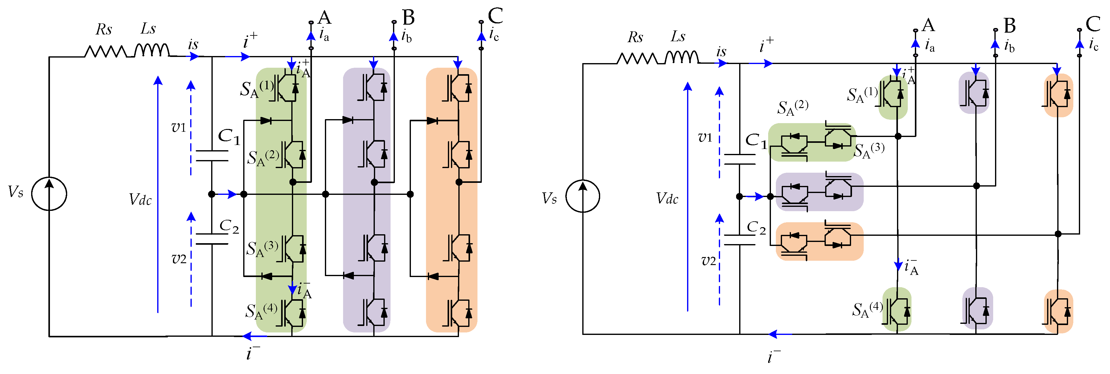
2.1. System Configuration

The circuit scheme of a three-level three-phase neutral point clamped inverter (NPC) is shown in Figure 1, for both conventional and T-type configurations. It consists of a DC voltage source (Vs) with series RL impedance, representing either a simplified model of a real DC source or a DC filter (series reactor). Each leg of the inverter is composed of four power switches (for leg A: SA(1) to SA(4), the same for legs B and C). Two capacitors C1 and C2 are connected to the neutral point of the inverter and serve as a voltage divider. For proper operation of the NPC inverter, the neutral point must be kept at one half of DC-link voltage by using a proper modulation strategy able to achieve voltage balancing between the capacitors.

2.2. Modulation Principles

In case of balanced modulation and within the linear modulation range, the output voltages normalized by Vdc and averaged over the switching period (Tsw = 1/fsw) correspond to the modulating signals [20]:
{ u A = m sin ( ϑ ) + C m = u A * + C m u B = m sin ( ϑ 2 π 3 ) + C m = u B * + C m u C = m sin ( ϑ 4 π 3 ) + C m = u C * + C m .
where ϑ = ωt, ω is the fundamental angular frequency (ω = 2πf), f is the fundamental frequency, m is the inverter modulation index, u i * are the normalized reference output voltages of each phase (i = A, B or C) and Cm represents the injected common mode signal.
The voltages across the two capacitors C1 and C2 can be spontaneously regulated to half of the DC-link voltage by the use of proper modulation technique with self-balancing capability. Correspondingly, the following averaged switching functions for the upper and lower switches S ¯ i ( 1 ) and S ¯ i ( 4 ) can be written (averaging is denoted by overline):
{ S ¯ i ( 1 ) = u i + | u i | S ¯ i ( 4 ) = u i + | u i | .
With reference to the modulation (1) and considering phase A, the averaged switching functions of the upper and the lower switches, Equation (2), become:
{ S ¯ A ( 1 ) = m sin ( ϑ ) + C m + | m sin ( ϑ ) + C m | S ¯ A ( 4 ) = m sin ( ϑ ) + C m + | m sin ( ϑ ) + C m | .
Due to the modulation symmetry among the three phases, the switching functions for the phases B and C are readily obtained considering the phase displacement of the normalized output voltages given in Equation (1).
In case of sinusoidal PWM (SPWM), the injected common-mode signal is zero:
C m = 0 .
However, in case of centered PWM (CPWM), the injected common-mode signal is:
C m = 1 2 ( max ( u A * , u B * , u C * ) + min ( u A * , u B * , u C * ) ) .
In this last case, Cm can be rewritten as:
C m = 1 2 m { sin ϑ , π 6 ϑ π 6 , 5 π 6 ϑ 7 π 6 sin ( ϑ + 2 π 3 ) , π 6 ϑ π 2 , 7 π 6 ϑ 3 π 2 sin ( ϑ 2 π 3 ) , π 2 ϑ 5 π 6 , 3 π 2 ϑ 11 π 6 .
A straightforward method to implement carrier-based optimized centered PWM (OCPWM) for three-phase three-level inverters has been proposed in [20]. The procedure is based on applying the traditional min/max centering separately to pivot voltages and residual two-level voltages. Pivot voltages are determined by a simple polarity combination of reference voltages. The resulting common-mode voltage that has to be injected in reference voltages is determined in few simple steps as described in the following equations:
C m = 1 2 ( max ( u A p , u B p , u C p ) + min ( u A p , u B p , u C p ) ) 1 2 ( max ( u A 2 L , u B 2 L , u C 2 L ) + min ( u A 2 L , u B 2 L , u C 2 L ) )
being
{ u A p = 1 4 [ s i g n ( u A * ) 1 3 ( s i g n ( u A * ) + s i g n ( u B * ) + s i g n ( u C * ) ) ] u B p = 1 4 [ s i g n ( u B * ) 1 3 ( s i g n ( u A * ) + s i g n ( u B * ) + s i g n ( u C * ) ) ] u C p = 1 4 [ s i g n ( u C * ) 1 3 ( s i g n ( u A * ) + s i g n ( u B * ) + s i g n ( u C * ) ) ]
{ u A 2 L = u A * u A p u B 2 L = u B * u B p u C 2 L = u C * u C p
Figure 2 shows the three carrier-based modulations considered in this paper.

3. Input Current Analysis

Input Current Components

With reference to Figure 1, the instantaneous input currents i+(t) and i(t) are composed of the averaged value over the switching period, i ¯ + and i ¯ , and the switching frequency component, Δ i + and Δ i . Similarly, i ¯ + and i ¯ consist of DC component over the fundamental period, Idc, and the alternating low-frequency component, i ˜ + and i ˜ , leading to:
{ i + ( t ) = i ¯ + + Δ i + = I d c + i ˜ + + Δ i + i ( t ) = i ¯ + Δ i = I d c + i ˜ + Δ i
In case of balanced load and neglecting the output current ripple, the corresponding three-phase output currents can be written as:
{ i a = I a c sin ( ϑ φ ) i b = I a c sin ( ϑ 2 π 3 φ ) i c = I a c sin ( ϑ 4 π 3 φ )
where Iac is the output current amplitude and φ is the power phase angle.
The averaged component (over the switching period) of each leg input current can be determined by multiplying the switching function of upper or lower switch of each phase by the corresponding output current. In the case of leg A it leads to:
{ i ¯ A + = S ¯ A ( 1 ) i a i ¯ A = S ¯ A ( 4 ) i a
By introducing Equations (3) and (11) in Equation (12), the averaged currents of the upper and lower switch of the leg A become:
{ i ¯ A + = I a c sin ( ϑ φ ) [ m sin ( ϑ ) + C m + | m sin ( ϑ ) + C m | ] i ¯ A = I a c sin ( ϑ φ ) [ m sin ϑ C m + | m sin ( ϑ ) + C m | ]
The total input currents i ¯ + and i ¯ can be calculated as the sum of the three leg currents as:
{ i ¯ + = S ¯ A ( 1 ) i a + S ¯ B ( 1 ) i b + S ¯ C ( 1 ) i c i ¯ = S ¯ A ( 4 ) i a S ¯ B ( 4 ) i b S ¯ C ( 4 ) i c
Due to the three-phase symmetry of modulation and output currents within the fundamental period T, both input currents have a periodicity of T/3. As a consequence, the analysis can be restricted to an angle range of 2π/3, and all the input harmonics are multiple of 3. i.e., apart from the DC component, the lowest harmonic order component is the 3rd.
With reference to the phase angle range 2π/3 ≤ ϑ ≤ 4π/3, two sub-ranges π/3 can be identified. Considering Equations (2), (11) and (14), the input currents i ¯ + and i ¯ can be expressed as:
i ¯ + = { S ¯ A ( 1 ) i a + S ¯ B ( 1 ) i b , 2 π 3 ϑ π S ¯ B ( 1 ) i b , π ϑ 4 π 3
i ¯ = { S ¯ C ( 4 ) i c , 2 π 3 ϑ π S ¯ A ( 4 ) i a S ¯ C ( 4 ) i c , π ϑ 4 π 3
Introducing Equations (1), (2), and (11) in Equations (15) and (16), and setting Cm = 0 as in case of SPWM, leads to:
i ¯ + = { m I a c [ 2 cos ( φ ) + cos ( 2 ϑ 2 π 3 φ ) ] ,   2 π 3 ϑ π m I a c [ cos ( φ ) + cos ( 2 ϑ π 3 φ ) ] ,   π ϑ 4 π 3
i ¯ = { m I a c [ cos ( φ ) cos ( 2 ϑ 2 π 3 φ ) ] ,   2 π 3 ϑ π m I a c [ 2 cos ( φ ) cos ( 2 ϑ π 3 φ ) ] ,   π ϑ 4 π 3
Similarly, replacing Equation (6) in Equation (1) in case of CPWM, input currents i ¯ + and i ¯ can be expressed as
i ¯ + = { m I a c 2 [ 3 sin ( 2 ϑ φ ) + sin ( π 6 + φ ) + 4 cos ( φ ) ] ,   2 π 3 ϑ 5 π 6 m I a c 2 [ 3 sin ( 2 ϑ π 3 φ ) sin ( φ π 6 ) + 4 cos ( φ ) ] , 5 π 6 ϑ π m I a c 2 3 [ cos ( 2 ϑ π 6 φ ) + cos ( φ + π 6 ) ] ,   π ϑ 7 π 6 m I a c 2 3 [ sin ( 2 ϑ φ ) + sin ( φ + π 3 ) ] , 7 π 6 ϑ 4 π 3
i ¯ = { m I a c 2 [ 3 sin ( 2 ϑ φ ) sin ( π 6 + φ ) + 2 cos ( φ ) ] ,   2 π 3 ϑ 5 π 6 m I a c 2 [ 3 sin ( 2 ϑ π 3 φ ) + sin ( φ π 6 ) + 2 cos ( φ ) ] , 5 π 6 ϑ π m I a c 2 [ 3 cos ( 2 ϑ π 6 φ ) 3 cos ( φ + π 6 ) + 6 cos ( φ ) ] ,   π ϑ 7 π 6 m I a c 2 [ 3 sin ( 2 ϑ φ ) 3 sin ( φ + π 3 ) + 6 cos ( φ ) ] , 7 π 6 ϑ 4 π 3
Although the above analytical calculations are based on SPWM and CPWM, the analysis could be readily extended to other PWM techniques, such as OCPWM, leading to more complex expressions not presented in this paper.
Consequently, the low-frequency input current components are readily determined in case of SPWM as:
I d c = 3 2 m I a c cos ( φ )
i ˜ + = { 1 2 m I a c [ cos ( φ ) + 2 cos ( 2 ϑ 2 π 3 φ ) ] ,   2 π 3 ϑ π 1 2 m I a c [ cos ( φ ) 2 cos ( 2 ϑ π 3 φ ) ] ,   π ϑ 4 π 3
i ˜ = { 1 2 m I a c [ cos ( φ ) + 2 cos ( 2 ϑ 2 π 3 φ ) ] ,   2 π 3 ϑ π 1 2 m I a c [ cos ( φ ) 2 cos ( 2 ϑ π 3 φ ) ] ,   π ϑ 4 π 3
In the case of CPWM, the low-frequency input currents are expressed as:
i ˜ + = { m I a c 2 [ 3 sin ( 2 ϑ φ ) + sin ( π 6 + φ ) + cos ( φ ) ] ,   2 π 3 ϑ 5 π 6 m I a c 2 [ 3 sin ( 2 ϑ π 3 φ ) sin ( φ π 6 ) + cos ( φ ) ] , 5 π 6 ϑ π m I a c 2 3 [ cos ( 2 ϑ π 6 φ ) + cos ( φ + π 6 ) 3 cos ( φ ) ] ,   π ϑ 7 π 6 m I a c 2 3 [ sin ( 2 ϑ φ ) + sin ( φ + π 3 ) 3 cos ( φ ) ] , 7 π 6 ϑ 4 π 3
i ˜ = { m I a c 2 [ 3 sin ( 2 ϑ φ ) + sin ( π 6 + φ ) + cos ( φ ) ] ,   2 π 3 ϑ 5 π 6 m I a c 2 [ 3 sin ( 2 ϑ π 3 φ ) sin ( φ π 6 ) + cos ( φ ) ] , 5 π 6 ϑ π m I a c 2 [ 3 cos ( 2 ϑ π 6 φ ) + 3 cos ( φ + π 6 ) 3 cos ( φ ) ] ,   π ϑ 7 π 6 m I a c 2 [ 3 sin ( 2 ϑ φ ) + 3 sin ( φ + π 3 ) 3 cos ( φ ) ] , 7 π 6 ϑ 4 π 3

4. Input Voltage Analysis

4.1. Input Voltage Components

Based on the analysis of the inverter input current ripple components, the instantaneous voltages v1 and v2 across DC-link capacitors can be written as:
{ v 1 = V 1 + v ˜ 1 + Δ v 1 v 2 = V 2 + v ˜ 2 + Δ v 2
where V1 and V2 are the DC components averaged over the fundamental period, v ˜ 1 and v ˜ 2 are the alternating low-frequency ripple components, and Δ v 1 and Δ v 2 are the switching frequency ripple components of the voltages across capacitors C1 and C2, respectively. Being the low-frequency ripple components widely studied in literature, the analysis is focused on the switching ripple component.

4.2. Peak-to-Peak Voltage Switching Ripple Evaluation

In order to calculate the voltage switching ripple of DC-link capacitors, the amount of the switching frequency component of currents Δi1 and Δi2 circulating through the DC-link capacitor C1 and C2 should be determined. Assuming that the DC source impedance at the switching frequency is much higher than the capacitor’s reactance, the whole current component Δi+ and Δi are circulating through the capacitors C1 and C2, i.e., Δi1 = Δi+ and Δi2 = Δi. In this case, the corresponding DC voltage variations (peak-to-peak) over the sub-periods [0–Δt1] and [0–Δt2] can be expressed as
Δ V 1 = 1 C 1 0 Δ t 1 Δ i + d t ,   Δ V 2 = 1 C 2 0 Δ t 2 Δ i d t .
being Δt1 and Δt2 specific switching time intervals. The instantaneous input current is considered constant within each considered time interval.
Due to the periodicity of the input currents i+ and i, the evaluation of peak-to-peak voltage ripple is limited to the phase angle range 2π/3 ≤ ϑ ≤ 4π/3. Analyzing the voltage ripple, two cases have been identified: the first case considering zero phase angle (φ = 0°) and the second considering φ = 60°. The peak-to-peak voltage switching ripple of capacitors has been analytically calculated as:
In case of φ = 0°:
Δ V 1 = T s w C 1 { ( 1 S ¯ A ( 1 ) ) i ¯ + , 2 π 3 ϑ 5 π 6 ( 1 S ¯ B ( 1 ) ) i ¯ + , 5 π 6 ϑ 4 π 3
Δ V 2 = T s w C 2 { ( 1 S ¯ C ( 4 ) ) i ¯ , 2 π 3 ϑ 7 π 6 ( 1 S ¯ A ( 4 ) ) i ¯ , 7 π 6 ϑ 4 π 3
In case of φ = 60°:
Δ V 1 = T s w C 1 { ( 1 S ¯ A ( 1 ) ) i ¯ + , 2 π 3 ϑ 5 π 6 ( i a + i b i ¯ + ) S ¯ A ( 1 ) , 5 π 6 ϑ π ( 1 S ¯ B ( 1 ) ) i ¯ + , 5 π 6 ϑ 4 π 3
Δ V 2 = T s w C 2 { ( 1 S ¯ C ( 4 ) ) i ¯ , 2 π 3 ϑ 7 π 6 ( i c i a i ¯ ) S ¯ C ( 4 ) , 7 π 6 ϑ 4 π 3
being S i ( 1 ) and S i ( 4 ) the switching function for the upper and lower switches of phase i (being i = A, B or C), given by Equation (2). The total averaged input currents i ¯ + and i ¯ can be calculated by Equations (17) and (18) in case of sinusoidal PWM, and by Equations (19) and (20) in case of centered PWM. In case of optimized centered PWM the input currents can be calculated introducing Equations (2), (7) and (11) in Equations (15) and (16), leading to more complex developments.
Equations (28)–(31) suggest normalization for ΔV1 and ΔV2, as follow:
Δ V 1 = I a c f s w C 1 Δ U 1 ,   Δ V 2 = I a c f s w C 2 Δ U 2 .
being ΔU1 and ΔU2 the normalized peak-to-peak voltage switching ripple amplitude of capacitors.
Figure 3 shows the distribution of the normalized peak-to-peak voltage switching ripple calculated based on Equations (28), (29), (30) and (31) over the period [0, 120°]. Two modulation indices have been selected, m = 0.3 and m = 0.5 and two output phase angles are considered, φ = 0 and φ = 60°.
Figure 3 presents the normalized peak-to-peak voltage ripple amplitude across the upper capacitor since the normalized peak-to-peak voltage ripple amplitude across the lower capacitor has exactly the same profile with a phase shift corresponding to 60° (1/2 of the considered period).
According to Figure 3, it can be seen a wide excursion of the normalized peak-to-peak voltage ripple amplitude, generally ranging between 0 (min) and 0.25 (max). Despite there are evident differences in the voltage switching ripple envelope profile among the three modulation strategies, it cannot be identified a modulation clearly better than the others from this point of view. This consideration is also supported by the diagrams presented in Figure 4, representing the maximum of the normalized peak-to-peak ripple amplitude, calculated numerically, over the whole modulation index range, for φ = 0°, 30°, 60°, and 90°, considering SPWM, CPWM, and OCPWM. Again, these three modulation techniques give similar and comparable results also with reference to the maximum of the peak-to-peak voltage switching ripple. For all the cases, the absolute maximum of normalized peak-to-peak voltage ripple amplitude can be assumed as 0.25.

5. Dc-link Preliminary Capacitor Design

Based on the analysis of capacitor voltage ripple components, simple and effective guidelines for a preliminary design of the capacitors C1 and C2 are proposed in this section. In particular, the capacitances can be calculated taking into account requirements or restrictions referred to the switching frequency and/or low-frequency voltage ripple components.
Despite the design of DC-link capacitors in the three-phase three-level inverter has been widely addressed in literature considering always the low-frequency voltage ripple, a guideline for the design of the DC-link capacitors for this multilevel inverter configuration based on the switching voltage ripple has not been developed yet.
In general, the capacitor voltage switching ripple amplitude could have additional specific restrictions to limit switching noise, electromagnetic interferences, and voltage stress on the DC-link.
In this paper, the selection of the DC-link capacitors C1 and C2 can be performed on the basis of the maximum amplitude of the peak-to-peak voltage switching ripple at the switching frequency (that is in the order of kHz).
According to Figure 4, it can be noted that the maximum amplitude of the peak-to-peak ripple is determined as:
Δ U 1 max = Δ U 2 max = 1 4
In this case, the capacitances can be readily calculated on the basis of Equations (32) and (33):
C 1 1 4 I a c f s w Δ V 1 max , C 2 1 4 I a c f s w Δ V 2 max

6. Results

In order to verify proposed theoretical developments valid for both the considered NPC multilevel inverter configurations (Figure 1), numerical simulations and corresponding experimental tests are carried out. Inverter is controlled by carrier-based multilevel PWM (Figure 2) with reference to the three considered modulation techniques (SPWM, CPWM, and OCPWM). The switching frequency is set 2.5 kHz to better emphasize the switching ripple components, and two different output phase angles (0 and 60°) are considered, as for the specific analytical developments. The main circuit parameters are summarized in Table 1 for both simulations and experiments.

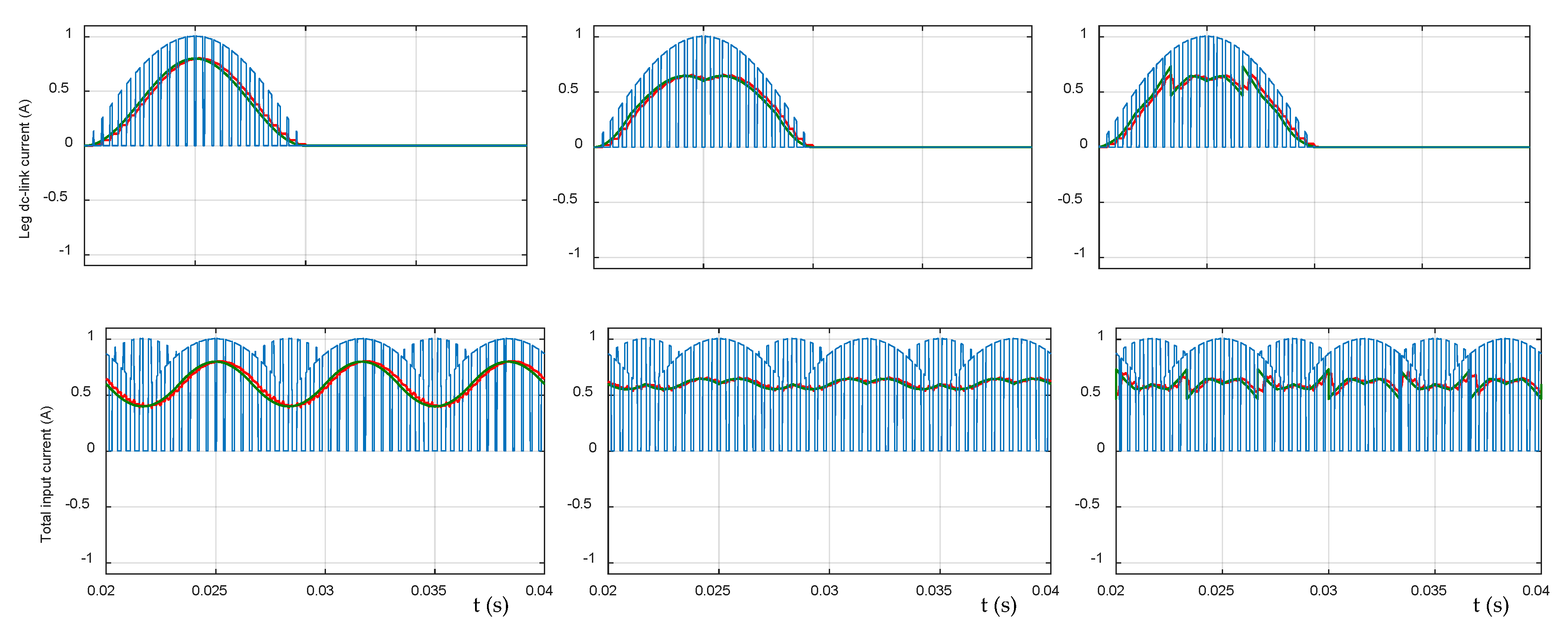
6.1. Simulation Results

Simulation results are carried out by implementing the power circuit scheme and the PWM techniques by Matlab/Simulink, considering SPWM, CPWM, and OCPWM.
The first simulation tests (Figure 5 and Figure 6) are concerning the input inverter currents. In this case, unity sinusoidal output current (Iac = 1A) are considered to easily verify the analytical developments presented in Section 3, with specific reference to the considered output phase angles φ = 0° and φ = 60°.
The top traces in Figure 5 and Figure 6 show the simulation results comparing the instantaneous input current of leg A i A + (blue trace) with its averaged value over the switching period i ¯ A + (red trace), and the corresponding low-frequency current component calculated by Equation (13) (green trace) in case of m = 0.4 and for two cases of output phase angles φ = 0° (Figure 5) and φ = 60° (Figure 6). The bottom traces in Figure 5 and Figure 6 show the total input current, with emphasis to instantaneous value i + (blue trace) and its averaged value over the switching period i ¯ + (red trace). The low-frequency current component (green trace) is determined analytically in both cases of SPWM and CPWM by Equations (22) and (24), respectively, and is calculated by replacing Equations (2), (7), and (11) in Equation (15), in the case of OCPWM.
The numerical results generally show a perfect matching with the theoretical values. The small delay between averaged and theoretical currents (Tsw/2) is due to the averaging process itself.
The second group of simulation tests is concerning the switching voltage ripple across the two DC-link capacitors. In this case, the load circuit model is corresponding to the real experimental setup, made with the purpose to easily adapt the output phase angles to the considered cases (φ = 0 and φ = 60°), according to Figure 7. The corresponding circuit parameters are given in Table 2.
The voltage switching ripple is determined by filtering away the low-frequency components form the instantaneous capacitor voltages.
Figure 8 presents the instantaneous voltage switching ripple across the capacitors (blue traces) in case of sinusoidal PWM together with the theoretical envelopes ±ΔV1/2 (upper capacitor) and ±ΔV2/2 (lower capacitor), analytically evaluated by (28) and (29) (red traces) for two cases of modulation index m = 0.3 (top) and 0.5 (bottom), considering the output phase angle φ = 0. The same quantities are presented in Figure 9 with reference to output phase angle φ = 60°. In this case, envelopes ±ΔV1/2 and ±ΔV2/2 are analytically evaluated by (30) and (31).
Similarly, Figure 10 and Figure 11 present the instantaneous voltage switching ripple across the capacitors (blue traces) in case of centered PWM together with the theoretical envelopes ±ΔV1/2 (upper capacitor) and ±ΔV2/2 (lower capacitor) (red traces) for two cases of modulation index m = 0.3 (top) and 0.5 (bottom), considering the output phase angles φ = 0 (Figure 10) and φ = 60° (Figure 11).
As mentioned in Section 4, the analytical developments could be readily extended to other more sophisticated modulation strategies, such as optimized centered PWM, but leading to more complex and less meaningful expressions. For this reason, the envelopes of voltage switching ripple have not explicitly obtained in case of OCPWM, just numerically derived introducing Equations (2), (7), (11), (15), and (16) in the basic Equations (28)–(31). Similarly, to previous cases, Figure 12 and Figure 13 present the instantaneous voltage switching ripple across the capacitors (blue traces) in case of optimized centered PWM together with the envelopes ±ΔV1/2 (upper capacitor) and ±ΔV2/2 (lower capacitor) (red traces) for two cases of modulation index m = 0.3 (top) and 0.5 (bottom), considering the output phase angles φ= 0 (Figure 12) and φ = 60° (Figure 13).

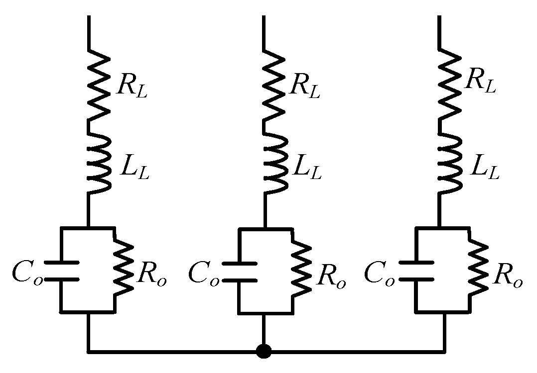
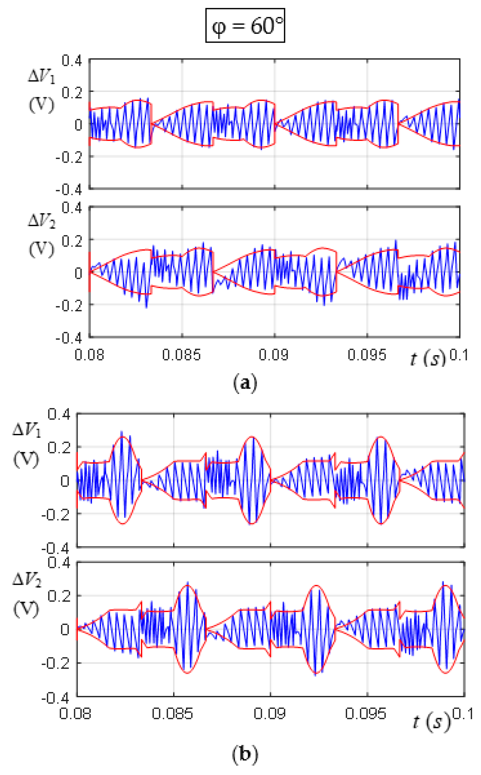
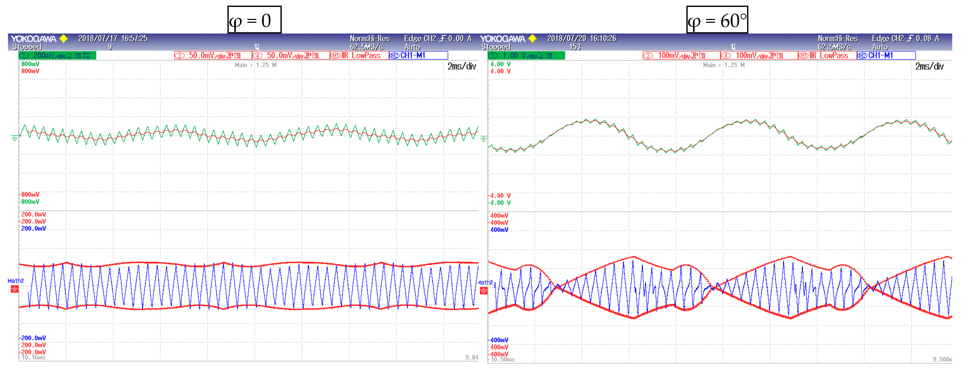
6.2. Experimental Results

A picture view of the whole experimental setup is shown in Figure 14. It consists of a three-phase T-type NPC inverter implemented by 12 discrete Silicon Carbide (SiC) power MOSFETs (CREE C2M0080120D) rated for 1200 V and 36 A. The three considered PWM techniques and the calculations to analytically determine the envelopes of voltage switching ripple across the two dc-link capacitors are implemented by a TMS320F28335 floating point DSP control board. Code Composer Studio (CCS) is adopted for programming the DSP board, with the possibility of real-time adjustment of modulation parameters by computer interface. The main circuit parameters are given in Table 1 and Table 2, i.e., the same used for the second group of simulations.
Experimental results are shown by Yokogawa DLM 2024 oscilloscope screenshots. Figure 15 presents an example of load voltage and current (blue and red traces, respectively) obtained by the laboratory setup in case of sinusoidal PWM and unity power factor (m = 0.5).
Figure 16 and Figure 17 present the results with reference to sinusoidal PWM and centered PWM techniques, respectively. Two values of modulation index: m = 0.3 and 0.5 (from top to bottom) and two values of the output phase angles φ = 0 and φ = 60° are considered (left and right column, respectively). In all screenshots, upper traces present the capacitor voltage and its averaged counterpart (blue and green traces, respectively) and the bottom traces present the measured capacitor voltage switching ripple and the calculated peak-to-peak envelopes provided by the DSP board and displayed using DAC block with a proper voltage scaling (red and green traces, respectively).
The capacitor voltage switching ripple has been obtained experimentally by simply using the “ac coupling” built-in function of the oscilloscope together with the built-in low-pass filter, on the basis of the instantaneous capacitor voltage, according to Equation (26).
Simulation and experimental results have a good matching for all the considered cases, as proved by comparing Figure 8 and Figure 9 with Figure 16 in case of SPWM and by comparing Figure 10 and Figure 11 with Figure 17 in case of CPWM. Note that the same scale is adopted in corresponding simulation and experimental di agrams to facilitate the comparison.

7. Conclusions

This paper deals with input current analysis and determination of capacitors voltage switching ripple in three-phase three-level neutral point clamped inverters. Reference is made to the basic modulation strategies, namely sinusoidal PWM, centered PWM, and optimized centered PWM, but the proposed method be easily extended to other modulation techniques. The switching frequency current and voltage ripple components have been analytically determined for the two dc-link capacitors. In particular, the peak-to-peak voltage ripple amplitudes have been calculated as a function of the inverter modulation index and the output current amplitude. Simple and effective guidelines for a preliminary design the dc-link capacitors of the NPC configuration have been also introduced. Developments have been carried out in case of general output power factor, representing either grid connections, motor, or passive loads.
The mathematical developments have been verified, both numerically and experimentally, for different values of modulation indices and specifically for two output phase angles φ = 0 (corresponding to most of the grid-connected applications) and φ = 60°. A very satisfactory matching between analytical, numerical, and experimental results has been achieved, proving the validity of the proposed approach.

Author Contributions

M.H. developed the theoretical analysis and the simulation results, also providing for the manuscript arrangement in cooperation with R.M. G.R. performed the experimental test and revised the manuscript, supported by M.H. and R.M. G.G. generally supervised and finalized the work.

Funding

This research received no external funding.

Conflicts of Interest

The authors declare no conflict of interest.

References

  1. Nabae, A.; Takahashi, I.; Akagi, H. A New Neutral-Point-Clamped PWM Inverter. IEEE Trans. Ind. Appl. 1981, 17, 518–523. [Google Scholar] [CrossRef]
  2. Giri, S.K.; Mukherjee, S.; Kundu, S.; Banerjee, S.; Chakraborty, C. A Carrier-Based PWM Scheme for Neutral Point Voltage Balancing in Three-Level Inverter Extending to Full Power Factor Range. IEEE J. Emerg. Sel. Top. Power Electron. 2017, 64, 1873–1883. [Google Scholar] [CrossRef]
  3. Liu, P.; Duan, S.; Yao, C.; Chen, C. A Double Modulation Wave CBPWM Strategy Providing Neutral-Point Voltage Oscillation Elimination and CMV Reduction for Three-Level NPC Inverters. IEEE Trans. Ind. Electron. 2018, 65, 16–26. [Google Scholar] [CrossRef]
  4. Dordevic, O.; Jones, M.; Levi, E. A Comparison of Carrier-Based and Space Vector PWM Techniques for Three-Level Five-Phase Voltage Source Inverters. IEEE Trans. Ind. Inform. 2013, 9, 609–618. [Google Scholar] [CrossRef]
  5. Petrella, R.; Pevere, A. Interleaved Carrier-Based Modulations for Reducing Low-Frequency Neutral Point Voltage Ripple in the Three-Phase Neutral Point Clamped Inverter. In Proceedings of the 2014 IEEE Applied Power Electronics Conference and Exposition APEC, Fort Worth, TX, USA, 16–20 March 2014; pp. 2386–2393. [Google Scholar]
  6. Xia, C.L.; Zhang, G.Z.; Yan, Y.; Gu, X.; Shi, T.N.; He, X.N. Discontinuous Space Vector PWM Strategy of Neutral-Point-Clamped Three-Level Inverters for Output Current Ripple Reduction. IEEE Trans. Power Electron. 2017, 32, 5109–5121. [Google Scholar] [CrossRef]
  7. López, I.; Ceballos, S.; Pou, J.; Zaragoza, J.; Andreu, J.; Ibarra, E.; Konstantinou, G. Generalized PWM-Based Method for Multiphase Neutral-Point-Clamped Converters with Capacitor Voltage Balance Capability. IEEE Trans. Power Electron. 2017, 32, 4878–4890. [Google Scholar] [CrossRef]
  8. Pevere, A.; Petrella, R. Discontinuous Hybrid Modulation Technique for Three-Phase Three-Level Neutral Point Clamped Inverters. In Proceedings of the 2013 IEEE Energy Conversion Congress and Exposition ECCE, Denver, CO, USA, 15–19 September 2013; pp. 3992–3999. [Google Scholar]
  9. Bianchi, N.; Di Pre, M. Active Power Filter Control Using Neural Network Technologies. IEE Proc. Electr. Power Appl. 2003, 150, 139–145. [Google Scholar]
  10. Vujacic, M.; Hammami, M.; Srndovic, M.; Grandi, G. Evaluation of DC Voltage Ripple InSingle-Phase H-Bridge PWM Inverters. In Proceedings of the IEEE 26th International Symposium on Industrial Electronics, Scotland, UK, 19–21 June 2017; pp. 711–716. [Google Scholar]
  11. Vujacic, M.; Hammami, M.; Srndovic, M.; Grandi, G. Theoretical and Experimental Investigation of Switching Ripple in the DC-Link Voltage of Single-Phase H-Bridge PWM Inverters. Energies 2017, 10, 1189. [Google Scholar] [CrossRef]
  12. Hammami, M.; Vujacic, M.; Grandi, G. Dc-Link Current and Voltage Ripple Harmonics in Three-Phase Three-Level Flying Capacitor Inverters with Sinusoidal Carrier-Based PWM. In Proceedings of the IEEE International Conference Industrial Technology, Lyon, France, 20–22 February 2018. [Google Scholar]
  13. Liang, Z.; Li, M.; Dong, Z.; Tian, S.; Li, K. Analytical Closed-Form Expressions of DC Current Ripple for Three-Level Neutral Point Clamped Inverters with Space-Vector Pulse-Width Modulation. IET Power Electron. 2016, 9, 930–937. [Google Scholar]
  14. Gopalakrishnan, K.S.; Das, S. Analytical Expression for RMS DC Link Capacitor Current in a Three-Level Inverter. In Proceedings of the Centenary Conference Electrical Engineering, Indian Institute of Science, Bangalore, India, 15–17 December 2011. [Google Scholar]
  15. Orfanoudakis, G.I.; Sharkh, S.M.; Yuratich, M.A. Analysis of Dc-Link Capacitor Current in Three-Level Neutral Point Clamped and Cascaded H-Bridge Inverters. IET Power Electron. 2013, 6, 1376–1389. [Google Scholar] [CrossRef]
  16. Pou, J.; Pindado, R.; Boroyevich, D.; Rodríguez, P. Evaluation of the Low-Frequency Neutral-Point Voltage Oscillations in the Three-Level Inverter. IEEE Trans. Ind. Electron. 2005, 52, 1582–1588. [Google Scholar] [CrossRef]
  17. Pou, J.; Zaragoza, J.; Rodríguez, P.; Ceballos, S.; Sala, V.M.; Burgos, R.P.; Boroyevich, D. Fast-Processing Modulation Strategy for the Neutral-Point-Champed Converter with Total Elimination of Low-Frequency Voltage Oscillations in the Neutral Point. IEEE Trans. Ind. Electron. 2007, 54, 2288–2294. [Google Scholar] [CrossRef]
  18. Fujii, K.; Kikuchi, T.; Koubayashi, H.; Yoda, K. 1-MW Advanced T-Type NPC Converters for Solar Power Generation System. In Proceedings of the 2013 15th European Conference on Power Electronics and Applications (EPE), Lille, France, 2–6 September 2013. [Google Scholar]
  19. Zhang, Z.; Anthon, A.; Andersen, M.A.E. Comprehensive Loss Evaluation of Neutral-Point-Clamped (NPC) and T-Type Three-Level Inverters Based on a Circuit Level Decoupling Modulation. In Proceedings of the 2014 International Power Electronics and Application Conference and Exposition PEAC, Shanghai, China, 5–8 November 2014. [Google Scholar]
  20. Grandi, G.; Loncarski, J. Simplified Implementation of Optimised Carrier-Based PWM in Three-Level Inverters. Electron. Lett. 2014, 50, 631–633. [Google Scholar] [CrossRef]
Figure 1. Circuit schemes of the three-phase three-level neutral point clamped (NPC) inverter: conventional type (left side) and T-type (right side).
Energies 11 03244 g001
Figure 2. Carrier-based PWM modulation logic for each leg (i) of NPC inverters: SPWM (red trace), CPWM (blue trace), and OCPWM (green trace) in case of m = 0.4. Underline denotes complementary.
Energies 11 03244 g002
Figure 3. Normalized peak-to-peak voltage ripple amplitude across the capacitors over the period [0, 120°] for two modulation indices m = 0.3 (a,b) and m = 0.5 (c,d) and output phase angles φ = 0 (a,c) (left) and 60° (b,d) (right) in case of SPWM (red), CPWM (blue) and OCPWM (green).
Energies 11 03244 g003
Figure 4. Maximum peak-to-peak value of the normalized voltage switching ripple vs. modulation index m in case of (a) sinusoidal pulse-width modulation (SPWM), (b) centered PWM (CPWM) and (c) optimized centered PWM (OCPWM) for different output phase angles.
Energies 11 03244 g004
Figure 5. One leg dc-link current (top) and total input current (bottom): instantaneous value (blue trace), its averaged value over the switching period (red), and calculated value (green) in case of SPWM, CPWM and OCPWM (from right to left) for m = 0.4, Iac = 1A and φ = 0°.
Energies 11 03244 g005
Figure 6. One leg dc-link current (top) and total input current (bottom): instantaneous value (blue trace), its averaged value over the switching period (red), and calculated value (green) in case of SPWM, CPWM and OCPWM (from right to left) for m = 0.4, Iac = 1A and φ = 60°.
Energies 11 03244 g006
Figure 7. Three-phase load circuit.
Energies 11 03244 g007
Figure 8. Capacitor voltage switching ripple (SPWM): simulation results (blue trace) and calculated peak- to-peak envelope (red traces) over a period for m = 0.3 (a) and m = 0.5 (b) in case of φ = 0°.
Energies 11 03244 g008
Figure 9. Capacitor voltage switching ripple (SPWM): simulation results (blue trace) and calculated peak- to-peak envelope (red traces) over a period for m = 0.3 (a) and m = 0.5 (b) in case of φ = 60°.
Energies 11 03244 g009
Figure 10. Capacitor voltage switching ripple (CPWM): simulation results (blue trace) and calculated peak- to-peak envelope (red traces) over a period for m = 0.3 (a) and m = 0.5 (b) in case of φ = 0°.
Energies 11 03244 g010aEnergies 11 03244 g010b
Figure 11. Capacitor voltage switching ripple (CPWM): simulation results (blue trace) and calculated peak- to-peak envelope (red traces) over a period for m = 0.3 (a) and m = 0.5 (b) in case of φ = 60°.
Energies 11 03244 g011
Figure 12. Capacitor voltage switching ripple (OCPWM): simulation results (blue trace) and calculated peak- to-peak envelope (red traces) over a period for m = 0.3 (a) and m = 0.5 (b) in case of φ = 0°.
Energies 11 03244 g012
Figure 13. Capacitor voltage switching ripple (OCPWM): simulation results (blue trace) and calculated peak- to-peak envelope (red traces) over a period for m = 0.3 (a) and m = 0.5 (b) in case of φ = 60°.
Energies 11 03244 g013
Figure 14. Picture view of the experimental setup.
Energies 11 03244 g014
Figure 15. Example of load voltage (blue) and current (red) for SPWM (m = 0.5, φ = 0°).
Energies 11 03244 g015
Figure 16. Experimental results for φ = 0° (left) and φ = 60° (right). Upper half: capacitor voltage and its averaged value. Lower half: calculated peak-to-peak envelope and measured capacitor voltage switching ripple with different modulation indexes: m = 0.3 and 0.5 (from top to bottom) in case of SPWM.
Energies 11 03244 g016
Figure 17. Experimental results for φ = 0° (left) and φ = 60° (right). Upper half: capacitor voltage and its averaged value. Lower half: calculated peak-to-peak envelope and measured capacitor voltage switching ripple with different modulation indexes: m = 0.3 and 0.5 (from top to bottom) in case of CPWM.
Energies 11 03244 g017aEnergies 11 03244 g017b
Table 1. Simulation/experiment circuit parameters.
LabelDescriptionParameters
VsDC voltage source100 V
RsDC source resistance5 Ω
LsDC source inductance10.15 mH
C1, C2DC-link capacitors1.12 mF
f, fsw fundamental and switching frequencies50 Hz, 2.5kHz
Table 2. Load parameters.
Loadφ = 0φ = 60°
RL3.16 Ω3.16 Ω
LL20.1 mH20.1 mH
Ro20 Ω0
Co58 μF0

