A Transformerless Single-Phase Current Source Inverter Topology and Control for Photovoltaic Applications


1
Department of Electronics Engineering, National Technological of Mexico-Technological Institute of Celaya, Celaya 38010, Mexico
2
Electronic Technology Department, King Juan Carlos University, 28933 Mostoles, Madrid, Spain
*
Author to whom correspondence should be addressed.
Energies 2018, 11(8), 2011; https://doi.org/10.3390/en11082011
Submission received: 31 May 2018
/
Revised: 26 July 2018
/
Accepted: 31 July 2018
/
Published: 2 August 2018
(This article belongs to the Special Issue Advanced Control Techniques for Power Converters)
Abstract
:Low power grid-tied photovoltaic (PV) generation systems increasingly use transformerless inverters. The elimination of the transformer allows smaller, lighter and cheaper systems, and improves the total efficiency. However, a leakage current may appear, flowing from the grid to the PV panels through the existing parasitic capacitance between them, since there is no galvanic isolation. As a result, electromagnetic interferences and security issues arise. This paper presents a novel transformerless single-phase Current Source Inverter (CSI) topology with a reduced inductor, compared to conventional CSIs. This topology directly connects the neutral line of the grid to the negative terminal of the PV system, referred as common mode configuration, eliminating this way, theoretically, the possibility of any leakage current through this terminal. The switches control is based on a hysteresis current controller together with a combinational logic circuitry and it is implemented in a digital platform based on National Instruments Technology. Results that validate the proposal, based on both simulations and tests of a low voltage low power prototype, are presented.
1. Introduction
Low-frequency transformers (50–60 Hz) between the conversion stage and the grid are often included in grid-tied photovoltaic (PV) systems. For security reasons, the grid neutral line and the chassis of the PV panel must be grounded. The transformer ensures that no leakage current flows between the grounded PV panels and the grounded grid neutral line. It also provides galvanic isolation and guarantees the absence of direct current (DC) injected from the PV system into the grid. However, the low-frequency transformer results in bulkier, heavier, and more expensive systems compared to transformerless ones. Finally, it also reduces the total efficiency of the system [1,2,3,4]. In order to eliminate these drawbacks, it can be used transformerless inverters. Unfortunately, in this case, a direct electrical connection between the PV panels ground and the grounded grid neutral line appears, due to the existing parasitic capacitances of the PV panels to ground. If a varying common-mode (CM) voltage, VCM, is generated by the conversion stage, a leakage current, or common-mode currents (icm), flows through the resulting equivalent circuit. This circuit is formed by the inverter and its output filter, the existing ground impedance ZGcGg and the parasitic capacitance CPVg between the PV panel and ground, as shown in Figure 1 [2,3,5]. This leakage current affects system efficiency, deteriorates the distortion of the grid current and the electromagnetic compatibility (EMC), and may cause security issues [5,6,7,8,9,10,11,12,13,14,15,16,17].
According to [2,3], VCM is defined as:
where v1N is the voltage difference between points “1” and “N”, v2N is the voltage difference between points “2” and “N” and, L1 and L2 are the output filter inductors.
Thus, the value of the leakage current mainly depends on the value of the parasitic capacitance of the PV system and the common-mode voltage, VCM, which is closely related to the inverter modulation strategy [6,7]. The PV panel and its frame structure, the surface and the distance between cells, the ambient conditions or the converter EMC filter are, among others, factors that affect to the value of the parasitic capacitance [8].
In order to minimize the generation of variable VCM voltages in transformerless PV systems, several solutions have been proposed: in [18], a review of several modulation strategies to suppress leakage currents is presented. Modulation techniques that do not produce a variable VCM, such us Bipolar Sinusoidal Pulse Width Modulation (BSPWM), are a possible solution [18]. Another option is isolating the PV system from the grid when VCM varies. Topologies such us H5, H6, HERIC and those shown in [19,20,21], have been proposed following this principle. Finally, other solutions propose the direct connection of the negative terminal of PV to the neutral line of the grid, referred here as common mode (CM). Such a configuration is proposed in [22]. It is worth mentioning that all these topologies are voltage source inverters (VSI).
Another option for a transformerless PV inverter is the Current Source Inverter (CSI). The voltage and current waveforms of this kind of inverters make them suitable for high power applications and adjustable speed drives. They also presents low EMC issues, low torque pulsations, and reduced stress on motors insulation. Fuel cells and wind turbine farms connected to the grid also uses CSI converters, since they present boost capability and permits parallel operation [23].
The CSI is also a natural candidate for transformerless PV inverters since they keep constant the value of the current at a defined set-point. In PV systems it is always desirable to have a Maximum Power Point Tracking (MPPT) algorithm in order to optimize the energy obtained from the PV panels. The PV panel current is one of the variables usually needed to implement an MPPT algorithm, so that the optimum value of the PV panel current can be used as the CSI current set-point.
Few CSI topologies for transformerless PV systems can be found in the literature. The Flying Inductor topology (FI), also known as the Karschny inverter, has the negative PV array connected directly to the neutral terminal of the grid, behaving almost as a CSI inverter in common mode configuration [24]. For this converter, the input voltage must be higher than the AC mains. Very recently, a modified FI with buck-boost capabilities has been presented [25]. The FI topology demands a high low-frequency input-current ripple from the PV panel, although it can be reduced with the appropriate design of the input capacitor placed in parallel with the PV panel. Recently, some CSI proposals for leakage current reduction have appeared in the literature. A transformerless CSI with low leakage current, based on the VSC H5 topology, is presented in [26]. In the same way, two transformerless three-phase CSI, based on the VSC H7 topology, are presented in [27,28]. These schemes are based on traditional differential mode inverters.
Following this trend, this paper presents a novel CSI topology with low leakage current, that could be considered a modified FI topology. It features low switching dv/dt and reliable protection against over-currents and short-circuits. The presented topology uses the common mode configuration, so the neutral line of the grid is connected directly to the negative terminal of the PV system, unlike the existing proposals. This connection maintains its voltage constant and negligible leakage current is generated, ideally zero. Another characteristic of this topology is that it allows the use of a smaller inductor L, compared to those usually found in conventional CSIs.
2. Proposed Topology
The circuit diagram of the proposed inverter is shown in Figure 2. It a based on a CSI in which, as mentioned before, the neutral line of the grid is connected directly to the negative terminal of the PV system. The output of the inverter is coupled to the grid through a CLC filter. It is composed of six power Metal-Oxide-Semiconductor Field-Effect Transistors (MOSFET) switches (S1, S2, S3, S4, S5 and S6) with a diode in series each, two capacitors (Cf and Cfout) and two inductors (L and Lf). Only two of the MOSFETs are conducting in each switching state.
2.1. Analysis of the CSI Converter
In order to analyze the topology, an equivalent subcircuit is obtained for each switching state of the inverter, depending on what switches are On or Off simultaneously. The proposed CSI can be in one of five states, as summarized in Table 1.
The equivalent subcircuits for each state are depicted in Figure 3.
2.1.1. Subcircuit 1
This subcircuit is defined by S1 and S4 turned on, and all other switches turned off (Figure 3a) This subcircuit generates the current for the positive half cycle of the output waveform. The inductor current iL increases in this stage if PV panel input voltage Vin is greater than filter capacitor voltage VCf. At the same time, VCf increases depending on the sign of iL − iLf, and filter current iLf increases if voltage VCf is greater than grid voltage Vout. Otherwise, all of them decrease. The state equations are:
2.1.2. Subcircuit 2
This subcircuit is defined by S2 and S3 turned on, and all other switches turned off (Figure 3b) This subcircuit generates the current for the negative half cycle of the output waveform. The inductor current iL increases in this stage if VCf is positive, otherwise decreases; filter capacitor voltage VCf decreases depending on the sign of iL + iLf, and filter current iLf increases if VCf is greater than Vout, otherwise decreases. The state equations are Equation (4) and:
2.1.3. Subcircuit 3
In this subcircuit, the switches S1 and S2 are turned on, and all other switches are turned off (Figure 3c). The inductor current iL increases and the filter capacitor voltage VCf decreases. The filter current iLf only increases if VCf is greater than Vout; if not, it decreases. No output current is generated in this stage. The state equations are Equation (4) and:
2.1.4. Subcircuit 4
In this subcircuit, the switches S5 and S6 are turned on, and all other switches are turned off (Figure 3d). The inductor current iL and the filter capacitor voltage VCf decreases. The filter current iLf only increases if VCf is greater than Vout; if not, it decreases. No output current is generated in this stage. The state equations are Equations (4) and (8):
2.1.5. Subcircuit 5
In this subcircuit, the switches S3 and S4 are turned on, and all other switches are turned off (Figure 3e). Ideally, the inductor current iL remains constant and the filter capacitor voltage VCf decreases. The filter current iLf only increases if VCf is greater than Vout; if not, it decreases. No output current is generated in this stage. The state equations are Equations (4) and (8):
Table 2 summarizes the significant voltages and currents for each subcircuit. It indicates under which conditions their values increase or decrease.
2.2. Model of the CSI Converter
In order to obtain a model of the converter, we define U1, U2, and U5 as the control laws for switches S1, S2, S3, S4, S5 and S6, according to Figure 2.
The model is obtained considering Equation (2) through Equation (13), as follows:
The capacitor Cout is not a state variable since it is at the same voltage as the grid.
2.3. Proposed Controller of the CSI Converter
For the modulation strategy of the proposed converter, Unipolar Sinusoidal Pulse Width Modulation (USPWM) has been chosen [18]. To do so, a sinusoidal modulator signal is compared with two symmetrical triangular carrier signals. Then, comparing the sinusoidal modulator signal with the upper triangular carrier, the auxiliary control signal A is obtained. In the same way, the auxiliary control signal B is obtained comparing the sinusoidal modulator signal with the lower triangular carrier.
Both signals A and B at a logic high level correspond to subcircuit 1, indicating that the output current iout will be positive. Both signals A and B at a low logic level correspond to subcircuit 2, indicating that the output current iout will be negative. Finally, both signals A and B at different logic levels correspond to any of the subcircuits 3, 4 or 5, indicating a zero output current iout. Subcircuits 1 and 2 increase or decrease the inductor current iL respectively. In order to maintain the iL current constant, as in any CSI converter, the controller has to select the appropriate subcircuit 3, 4 or 5.
So, subcircuits 1 and 2 are in charge of providing the output current iout, while subcircuits 3, 4 and 5 are responsible for keeping constant the inductance current iL.
All these waveforms are shown in Figure 4. Note that two low-frequency triangular carrier signals have been used only to better illustrate the operation.
2.3.1. Inductor Current Control
The current controller consists of a hysteresis controller along with a zero output current selector subcircuit. For the hysteresis controller, it has to be defined a value for the current hysteresis band, around the constant value of the inductor current iL. When the current iL is higher or lower than desired, a high logic level signal PE or NE is generated respectively, by means of two comparators. These signals together with a signal , coming for the zero output current subcircuit selector, generates signal F. This signal will be used as an input to select the appropriate zero output current subcircuit 3 or 4, in order to increase or decrease current iL. The hysteresis controller associated circuitry is shown in Figure 5.
It has to be noticed that although the hysteresis controller is a frequency variable control, its output signal F is the input to a bi-stable of the zero output current selector subcircuit which is clocked by the Sinusoidal Pulse Width Modulation (SPWM) signal, resulting, then, in a constant switching frequency.
The zero output current selector subcircuit detects any zero output current ipwm state. To do so, an XOR function of signals A and B is performed, obtaining an auxiliary output signal C. This signal is at a high logic level at any zero output current ipwm and is also used as the CLK input to a D-type positive edge triggered flip-flop, which will divide the frequency of C by half. The input of the D-type flip-flop is signal F, coming from the hysteresis controller. The output signal Q allows differentiating two cases for the zero output current state. Signal Q at a high logic level indicates that subcircuit 3 must be used, and signal Q at a low logic level indicates that subcircuit 4 must be used.
Therefore, this current controller allows to increase and decrease the current iL during the zero output current sates in order to keep iL constant. These signals and the associated logic circuit are shown in Figure 6 (a low-frequency signal was used to illustrate the operation).
It has to be noticed that the selection of the appropriate zero output current ipwm state depends on changes of signals A and B. During the sinusoidal output current zero crossing, both signals A and B do not change in an interval. During this interval, it is not possible to change the state of charge or discharge of the inductance L, so the current iL will remain increasing or decreasing according to the last zero output current state selected. This may cause an overcurrent, as seen in Figure 7. The length of this interval depends mainly on the frequency of the SPWM carrier signal and to a lesser extent on the amplitude modulation index. This drawback can be overcame increasing the SPWM carrier signal frequency, at a higher cost in switching losses; increasing the value of the inductance L to limit the maximum current iL, at a higher cost in size and weight of this inductance; or oversizing the nominal current of the switches. Alternatively, a new control with an independent second hysteresis band can be designed, at a higher cost in control complexity.
2.4. CSI Converter Synthesis
The design criteria for the different components of the converter are detailed. A low voltage low power prototype has been built and tested following these design guidelines. Since the main purpose is to validate the topology and the proposed control, it is not an optimized design in terms of efficiency, size, and weight.
2.4.1. Inductor
It is desirable to have the minimum possible inductor L. It has to be large enough to store energy to maintain an average constant value of the iL current, and to limit its excursion as close as possible to the hysteresis band. Its design has to take into account the worst case of operation, corresponding to a change from subcircuit 3 to subcircuit 1, in which the inductor current iL increases, as shown in Figure 9. Equations (17) and (18) determine the necessary inductance Ls3 and Ls1 to limit the maximum value of the increment of iL (ΔiL) at each stage, derived from Equations (2) and (7), respectively:
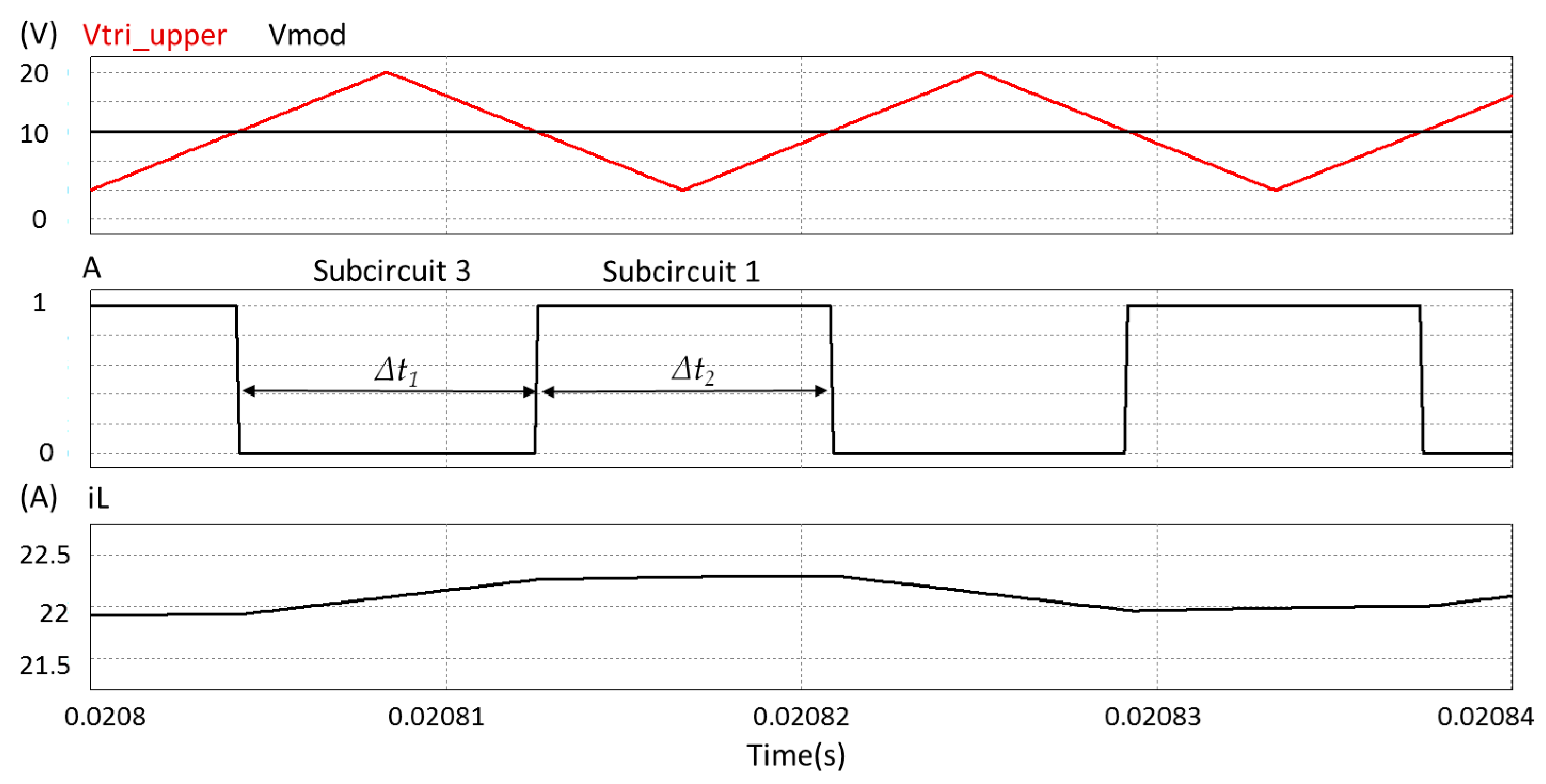
where Δt1 and Δt2 are the duration of subcircuits 3 and 1 respectively. These stages are consecutive, both contribute to ΔiL, so the necessary L is obtained by adding Equations (17) and (18), resulting in Equation (19):
It can be observed that the contribution of subcircuit 3 to iL is higher than the contribution of subcircuit 1. The time Δt1 is maximum at the peak of the sinusoidal modulator signal and depends on the modulation index of the SPWM. At low modulation indexes, subcircuit 3 stage is longer than at high modulation indexes. A conservative value of 0.5 for the modulation index can be taken as design criteria.
For an input voltage Vin = 200 V, average current iL = 22 A, hysteresis band of 0.02 A, switching frequency fsw = 60 kHz, modulation signal fgrid = 60 Hz and modulation index of 0.5; a value of Δt1 ≈ Δt2 = 10 μs is obtained by simulation. With a ΔiL = 0.5 A (2.5% of iL) results in an inductance of approximately 5 mH.
As mentioned in Section 2.3.1, during the sinusoidal output current iout zero crossing an overcurrent may occur. For the proposed values, the overcurrent interval lasts up to 50 μs, the value was obtained by simulation, and an overcurrent of ΔiL ≈ 2.5 A may be expected.
An alternative criteria design for inductance L is to limit this maximum current iL. A worst case would be subcircuit 3, Equation (17), with the aforementioned value of Δt1 ≈ 50 μs obtained by simulation, resulting in an inductance L of approximately 10 mH.
2.4.2. Output Filter
For reducing current ripple provoked by PWM high-frequency switching and improve Total Harmonic Distortion (THD) of the output current iout, it is necessary an output filter. A CLC filter has been implemented. It consists of a conventional CL filter plus an additional capacitor Cout on the grid side. This configuration shows better performance with smaller size and capacity compared to a CL filter. A detailed analysis and calculation method, including filter resonance, damping methods, and grid inductance influence can be found in [29]. As a simplified approach, a CL filter can be first calculated [30]. Equations (20) and (21) are the current function transfer GCL and cut-off frequency fcoff, respectively, for an ideal non-dumped filter, although a small series dumping effect is always present due to capacitors ESR and inductance winding resistance:
For a switching frequency of fsw = 60 kHz, a cut-off frequency fcoff = 1.5 kHz, and selecting a Cf = 5 μF film capacitor, an inductance Lf = 2 mH is obtained. A Cout = 0.1 μF capacitor is then added, taking into account that the two resonance frequencies of a CLC filter are related to all components values of the filter (Cf, Lf, Cout and grid variable inductance) [29]. These values are validated by simulation.
2.4.3. Semiconductors Selection
In CSI converters, the semiconductors for the switches must be unidirectional in current, so if MOSFETs are selected, a series diode must be included. Another option is the use of single Insulated Gate Bipolar Transistors (IGBT) as switches (without anti-parallel diode), reducing the number of components and increasing system reliability since no series diodes are needed. Regarding efficiency, it should be evaluated if two low loss semiconductors in series, such as SiC MOSFETs and SiC diodes, offer a better performance than a single IGBT.
In the prototype developed, Si MOSFETs and diodes have been used because of the availability of these components. For the currents and voltages expected, <5 A and <230 V respectively, an IRF840 MOSFET (8 A, 500 V, RDS = 0.85 Ω, Fairchild Semiconductor Corporation, Sunnyvale, CA, USA) and a MUR840 diode (8 A, 400 V, Fairchild Semiconductor Corporation, Sunnyvale, CA, USA) have been selected.
2.4.4. Comparison with Other CSI Schemes
Comparing the proposed converter with other CSI topologies, it can be found that a significant reduction in the inductor L is achieved. A general classification of CSI can be found in [31]. For Multilevel Paralleled CSI, the design criteria for the inductor is the energy stored in order to maintain the output current, resulting in large inductors of 400 mH for inductor currents of 0.5 A [31]. The Multilevel Two-stages CSI uses two inductors, the input and the balanced inductor, of 600 mH and 60 mH respectively, for currents of 2 A. These inductors can be reduced at higher currents, but its value still remains high [32]. The Embedded Multilevel CSI uses two balance inductors of 45 mH each, and an input inductor of 105 mH for a total current of 18 A [33]. The PWM CSI has values of 80 mH for inductor currents of 10 A [34]. A modified PWM CSI topology allows reductions of the inductor up to 7 mH for inductor currents of 91 A [35]. Also, the reduction can be obtained by means of the switching strategies, resulting in inductors of 30 mH for 9 A currents [36].
Note that for the same current of the PWM CSI of [34] and keeping ΔiL = 2.5% of iL, and approximately inductance of 750 μH results. Also note that none of these topologies deal with leakage current reduction. Recently, some proposals for leakage current reduction have appeared. A transformerless CSI with low leakage current, based on the VSC H5 topology, is presented in [26], with an inductor of 8 mH for inductor currents of 8 A. It concludes that for an inductor reduction, higher switching frequencies should be achieved by means of SiC devices, and then the leakage current may be an important issue. In the same way, two transformerless three-phase CSI, based on the VSC H7 topology, are presented in [27,28]. A reduced inductor of 2 mH, but without information regarding the inductor current, is used in [27]. Two different modulation strategies are presented in [28], with an inductor of 2 mH for inductor currents of 8 A. Table 3 summarizes the significant values of the CSI schemes compared.
As it can be observed in the table, the proposed topology offers the best leakage current reduction since it uses the common mode configuration. Some of the other schemes also have low values for leakage currents, but not as low as the proposed one, since they all are based on traditional differential mode inverters.
3. Simulation and Prototype Test Results
The proposed system was first numerically simulated and then tested in a low power prototype, in order to confirm the feasibility of the proposed system.
3.1. Simulations Results
A simulation using PSIM© (Version 11.1, Powersim Inc., Rockville, MD, USA) was performed for the circuit of Figure 2, in which the CSI inverter is connected to the grid. Parameter values for the simulation are shown in Table 4.
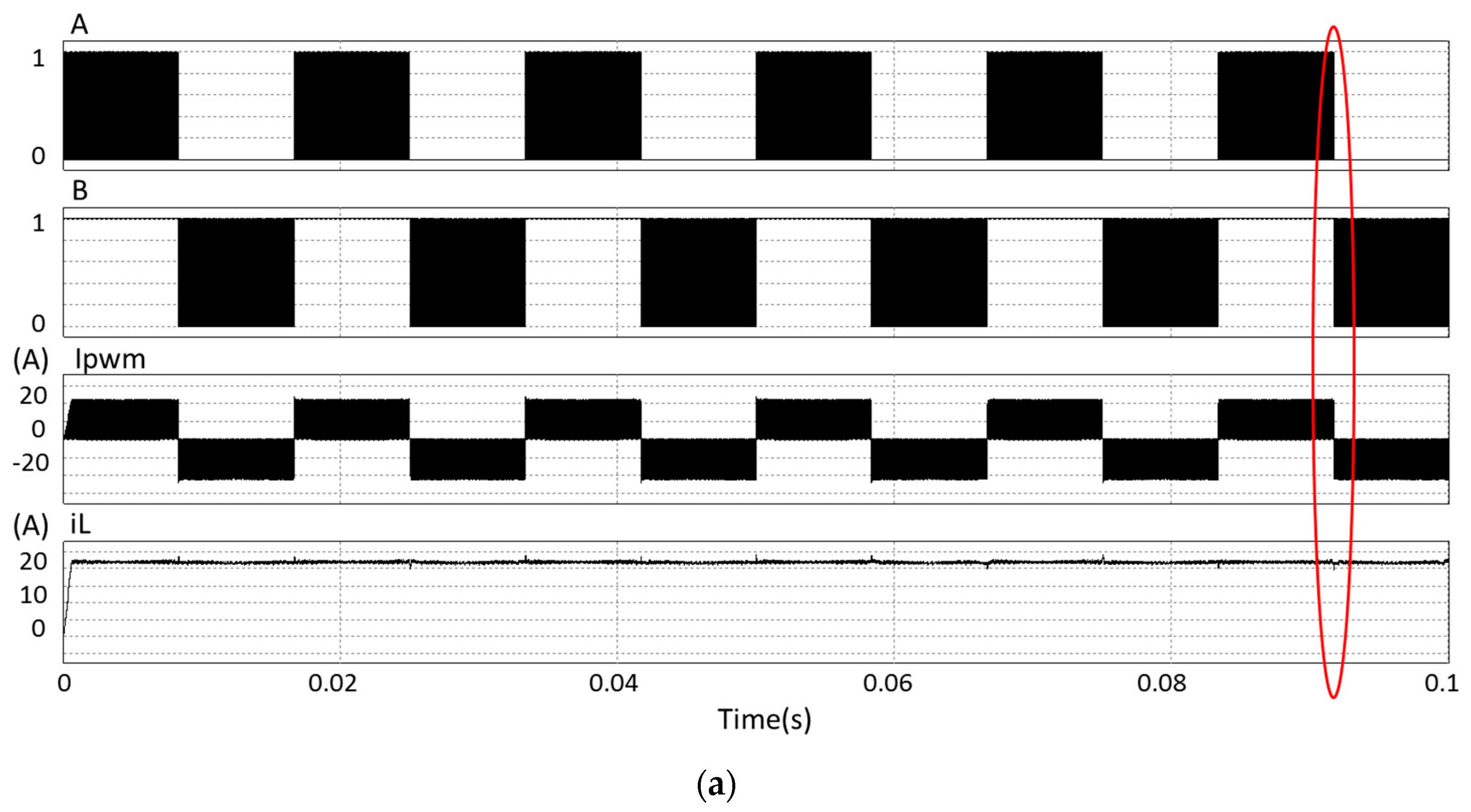
The operation of the proposed hysteresis controller shown in Figure 10. Figure 10a shows several periods of auxiliary control signals A and B, the resulting output current before de CLC filter, ipwm, and the inductor current iL, in order to illustrate the steady state operation of the system. Figure 10b shows a zoom of the rounded area in Figure 10a. It can be observed that the system operates as expected. The signals Vout, iout, and iL are shown in Figure 11. As it can be observed, the current of the inductor L is controlled around the desired level by means of the hysteresis band, except during the sinusoidal output current iout zero crossing, where an overcurrent occurs, although always within acceptable limits. The voltage and the current are operated with a CLC filter. The output signals can be viewed clearly sinusoidal and in phase. The THD of the output current at steady state is 1.8%.
The leakage current in the solar panel is under 15 mA for a conservative value of the parasitic capacitance CPVg = 5 nF every 200 W, that makes a total of 25 nF for an array of panels of 1 kW, as it can be seen in Figure 12.
3.2. Prototype Test
The proposed system was designed and built. The controller was implemented on an electronic board based on the National Instruments technology. The platform considered was the General Purpose Inverter Controller (GPIC), together with the LabVIEW visual programming software. The protections have been also programmed.
3.2.1. Controller Stage
The first component of the implemented controller in the LabVIEW software (2016 version, National Instruments Corporation, Austin, TX, USA) is the input/output block. The grid voltage Vline and the inductor current iL are sensed by means of the LEM LV25-P and LTS 25-NP voltage and current sensors, respectively. These signals are read by the GPIC. Also, the output signal for driving the switches are implemented. The current reference, free of distortions and synchronized with the grid, was generated by means of a Second Order Generalized Integrator-Frequency Looked Loop (SOGI-FLL). The amplitude was normalized, in order to avoid the dependency from the input voltage variations, and a measurements offset elimination stage was also added. A soft-start has also been implemented, to avoid high currents at the start-up of the power stage. It consists of an AC mains zero crossing detector that triggers the start-up of the converter. The switches control signals are generated following a USPWM pattern. The sinusoidal signal reference, synchronized with the grid, comes from de SOGI-FL, and the triangular carrier signals are at a frequency of 60 kHz. As it was mentioned before, a combinational circuit and a hysteresis controller is employed to regulate the current of the inductor L, iL, selecting the appropriate subcircuit according to the Table 2. SPWM, the hysteresis controller, the control signals A, B, F and Q, subcircuit switches selection and overlapping time are generated by logic blocks implemented on the GPIC platform. One of the main advantages of using LabVIEW is that a friendly-user interface can be easily implemented. It allows to fix the converter control parameters, such as the current protection, the desired inductor current iL level (set point), the width of the hysteresis band or the soft-start operation; and also some signals can be shown, to monitor the status of the converter. A diagram of the blocks of the controller is shown in Figure 13.
3.2.2. Experimental Test
A low power prototype was implemented, just to illustrate the operation of the proposed topology and control. A PV panel simulator E4361A from Agilent Technologies was used to generate the input voltage Vin. This simulator generates a maximum output voltage of 60 V and a maximum output current of 4.25 A, so maximum available voltage and power are bounded.
Parameter values for the prototype are shown in Table 5.
First, the prototype was tested with a resistive load. Figure 14 and Figure 15 show the main waveforms and output current iout distortion, for an inductance current iL of 1 A and 3 A, respectively. A hysteresis band of 0.2 A was selected. The THD of the output current was measured with a 1735 Power Logger Analyst (FLUKE, Everett, WA, USA). As it can be seen, the converter operates as expected. At this low voltage, overcurrents in iL are negligible. A THD of 2.8% was obtained for the last test.
The performance of the converter under a sudden change in the set point of the inductor current iL is illustrated in Figure 16. A step from 1 A to 3 A and viceversa is forced. A hysteresis band of 0.2 A was selected. The settling time was 784 μs and 260 μs respectively.
The prototype was also tested connected to the grid, as shown in Figure 2. A sudden change in the set point of the inductor current iL was conducted. Figure 17 shows the output current and the grid voltage during this test.
It has to be noted that there is no direct control of the output current iout, so the THD can be high when connected to the grid. Additional control strategies may be proposed to reduce the output current distortion.
3.2.3. Power Losses Estimation
The conduction losses of the power stage can be determined considering the simplified circuit is shown in Figure 18. This is possible since there are always two switches conducting at the same time, and the inductor current iL is kept constant (the ripple is disregarded). The switches have been implemented with a MOSFET and a diode in series. If an IGBT without diode in anti-parallel is considered, the series diode should be removed.
The power losses, including the switching losses, are determined by:
where rL is the parasitic resistance of the inductor L; VD is the diode forward voltage; rDSon is the MOSFET ON resistance; VDS is the MOSFET Drain-Source voltage; tr and tf are the rise and fall time of the main semiconductors, respectively; and fsw is the switching frequency.
The measured rL is 0.4 Ω. Τhe components selected are Si semiconductors, with VD = 1.1 V, VDS = 35 V, rDSon = 850 mΩ tr = 35 ns, tf = 30 ns, and fsw = 60 kHz, the estimated power losses are 4.57 W. However, changing VDS = 200 V, the losses are incremented to 5.86 W and considering a grid voltage of 127 V, the resulting estimated efficiency is 88.45%.
With equivalent SiC semiconductors, the values are now VD = 0.8 V, VDS = 35 V, rDSon = 16 mΩ, tr = 11 ns, tf = 10 ns and fsw = 60 kHz, the estimated power losses are 2.41 W. And, considering VDS = 200 V, the losses are incremented to 2.82 W, if the grid voltage is 127 V, the resulting estimated efficiency is 94.08% respectively. Figure 19 shows an estimated loss breakdown figures for both Si and SiC semiconductors for these last conditions.
As it can be seen, the losses in the diodes are the main contributor to total losses, so, as mentioned in Section 2.4.3, a solution with an IGBT switches without antiparallel diode should be considered for a practical implementation. It has been taken into account that, as mentioned in Section 3.2.2.
4. Conclusions
There are many works on topologies of transformerless PV converters, trying to reduce the leakage current at the ground connection. One of the most successful technique is the common mode configuration, in which the neutral line of the grid directly connects to the negative terminal of the PV system. However, most of them are based on VSI converters. This paper proposes a new topology for a CSI converter with reduced leakage currents in common mode configuration. A complete analysis, design, and operation were presented. A new controller has been also designed and implemented. A 1 kW system simulation has been carried out, but also a low power prototype has been built and tested in order to confirm the feasibility of the proposed system. The system has a leakage current under 15 mA and low output current THD, <3%. Efficiency has been estimated, with reasonable numbers, although converter design was intended to test the topology proposed and the control, and it was not optimized for reduced losses. Finally, the inductor L is smaller than those usually found in conventional CSIs. The obtained results show that this proposal is suitable for PV converters connected to the AC mains.
Author Contributions
The authors contribute to the whole work. J.C., N.V., C.H. and J.V. worked on the converter topology, controller design, implementation, and testing. N.V. and J.V. supervised the paper writing and reviewing.
Funding
This research was partially funded by the SINFOTON-CM: S2013/MIT-2790 program from the Comunidad de Madrid, Spain, and by the National Instruments Corporation through the 2016 NI Academic Research Grant program. By the Mexican side, this work was sponsored by CONACyT under project No. 293557.
Conflicts of Interest
The authors declare no conflict of interest. The founding sponsors had no role in the design of the study; in the collection, analyses, or interpretation of data; in the writing of the manuscript, and in the decision to publish the results.
References
- Zhang, L.; Siui, K.; Xing, Y.; Xing, M. H6 Transformerless Full-Bridge PV Grid-Tied Inverters. IEEE Trans. Power Electron. 2014, 29, 1229–1238. [Google Scholar] [CrossRef]
- Gu, Y.; Li, W.; Zhao, Y.; Yang, B.; Li, C.; He, X. Transformerless Inverter with Virtual DC Bus Concept for Cost-Effective Grid-Connected PV Power Systems. IEEE Trans. Power Electron. 2013, 28, 793–805. [Google Scholar] [CrossRef]
- Gubra, E.; Sanchis, P.; Ursua, A.; Lopez, J.; Marroyo, L. Ground currents in single-phase transformerless photovoltaic systems. Prog. Photovolt. Res. Appl. 2007, 15, 629–650. [Google Scholar] [CrossRef] [Green Version]
- Gonzalez, R.; Gubia, E.; Lopez, J.; Manrroyo, L. Transformerless Single-Phase Multilevel-Based Photovoltaic Inverter. IEEE Trans. Ind. Electron. 2008, 55, 2694–2702. [Google Scholar] [CrossRef]
- Gu, B.; Dominic, J.; Lai, J.-S.; Chen, C.-L.; LaBella, T.; Chen, B. High reliability and efficiency single-phase transformerless inverter for grid-connected photovoltaic systems. IEEE Trans. Power Electron. 2013, 28, 2235–2245. [Google Scholar] [CrossRef]
- Vázquez, N.; Rosas, M.; Hernández, C.; Vázquez, E.; Perez-Pinal, F.J. A New Common-Mode Transformerless Photovoltaic Inverter. IEEE Trans. Ind. Electron. 2015, 62, 6381–6391. [Google Scholar] [CrossRef]
- Li, W.; Gu, Y.; Luo, H.; Cui, W.; He, X.; Xia, C. Topology review and derivation methodology of single-phase transformerless photovoltaic inverters for leakage current suppression. IEEE Trans. Ind. Electron. 2015, 62, 4537–4551. [Google Scholar] [CrossRef]
- Kerekes, T.; Teodorescu, R.; Liserre, M. Common mode voltage in case of transformerless PV inverters connected to the Grid. In Proceedings of the 2008 IEEE International Symposium on Industrial Electronics, Cambridge, UK, 30 June–2 July 2008. [Google Scholar]
- Kerekes, T.; Todorescu, R.; Rodríguez, P.; Vázquez, G.; Aldabas, E. A new high-efficiency single-phase transformerless PV inverter topology. IEEE Trans. Ind. Electron. 2011, 58, 184–191. [Google Scholar] [CrossRef] [Green Version]
- Xiao, H.; Xie, S. Transformerless split-inductor neutral point clamped three-level PV grid-connected inverter. IEEE Trans. Power Electron. 2012, 27, 1799–1808. [Google Scholar] [CrossRef]
- Bae, Y.; Kim, R.-Y. Suppression of common-mode voltage using a multicentral photovoltaic inverter topology with synchronized PWM. IEEE Trans. Ind. Electron. 2014, 61, 4722–4733. [Google Scholar] [CrossRef]
- Ji, J.; Wu, W.; He, Y.; Lin, Z.; Blaabjerg, F.; Chung, H.S.-H. A simple differential mode EMI suppressor for the LLCL-filter-based single-phase grid-tied transformerless inverter. IEEE Trans. Ind. Electron. 2015, 62, 4141–4147. [Google Scholar] [CrossRef]
- Xiao, H.; Xie, S. Leakage current analytical model and application in single-phase transformerless photovoltaic grid-connected inverter. IEEE Trans. Electromagn. Compat. 2010, 52, 902–913. [Google Scholar] [CrossRef]
- Yu, W.; Lai, J.-S.J.; Qian, H.; Hutchens, C. High-efficiency MOSFET inverter with H6-type configuration for photovoltaic nonisolated AC-module applications. IEEE Trans. Power Electron. 2011, 26, 1253–1260. [Google Scholar] [CrossRef]
- López, Ó.; Freijedo, F.D.; Yepes, A.G.; Fernández-Comesaña, P.; Malvar, J.; Teodorescu, R.; Doval-Gandoy, J. Eliminating ground current in a transformerless photovoltaic application. IEEE Trans. Energy Convers. 2010, 25, 140–147. [Google Scholar] [CrossRef]
- Salmi, T.; Bouzguenda, M.; Gastli, A.; Masmoudi, A. A novel transformerless inverter topology without zero-crossing distortion. Int. J. Renew. Energy Res. 2012, 2, 140–146. [Google Scholar]
- López, Ó.; Teodorescu, R.; Freijedo, F.; DovalGandoy, J. Leakage current evaluation of a singlephase transformerless PV inverter connected to the grid. In Proceedings of the APEC 07—Twenty-Second Annual IEEE Applied Power Electronics Conference and Exposition, Anaheim, CA, USA, 25 February–1 March 2007. [Google Scholar]
- Shi, X.; Tang, T.; Xu, J.; Huang, R.; Xie, S.; Kan, J. Leakage current elimination mechanism for photovoltaic grid-tied inverters. In Proceedings of the IECON 2013—39th Annual Conference of the IEEE Industrial Electronics Society, Vienna, Austria, 10–13 November 2013. [Google Scholar]
- Xiao, H.F.; Liu, X.P.; Lan, K. Zero-Voltage-Transition Full-Bridge Topologies for Transformerless Photovoltaic Grid-Connected Inverter. IEEE Trans. Ind. Electron. 2014, 61, 5393–5401. [Google Scholar] [CrossRef]
- Araujo, S.V.; Zacharias, P.; Mallwitz, R. Highly Efficient Single-Phase Transformerless Inverters for Grid-Connected Photovoltaic Systems. IEEE Trans. Ind. Electron. 2010, 57, 3118–3128. [Google Scholar] [CrossRef]
- Cui, W.; Yang, B.; Zhao, Y.; Li, W.; He, X. A novel single-phase transformerless grid-connected inverter. In Proceedings of the IECON 2011—37th Annual Conference of the IEEE Industrial Electronics Society, Melbourne, VIC, Australia, 7–10 November 2011. [Google Scholar]
- Vazquez, N.; Vazquez, J.; Vaquero, J.; Hernandez, C.; Vazquez, E.; Osorio, R. Integrating Two Stages as a Common-Mode Transformerless Photovoltaic Converter. IEEE Trans. Ind. Electron. 2017, 64, 7498–7507. [Google Scholar] [CrossRef]
- Morsy, A.S.; Ahmed, S.; Enjeti, P.; Massoud, A. An active damping technique for a current source inverter employing a virtual negative inductance. In Proceedings of the 2010 Twenty-Fifth Annual IEEE Applied Power Electronics Conference and Exposition (APEC), Palm Springs, CA, USA, 21–25 February 2010. [Google Scholar]
- Karschny, D. Wechselrichter. German Patent DE 19 642 522 (C1), 23 April 1998. [Google Scholar]
- Azary, M.T.; Sabahi, M.; Babaei, E.; Meinagh, F.A.A. Modified Single-Phase Single-Stage Grid-Tied Flying Inductor Inverter with MPPT and Suppressed Leakage Current. IEEE Trans. Ind. Electron. 2018, 65, 221–231. [Google Scholar] [CrossRef]
- Guo, X. A Novel CH5 Inverter for Single-Phase Transformerless Photovoltaic System Applications. IEEE Trans. Circuits Syst. Express Briefs 2017, 64, 1197–1201. [Google Scholar] [CrossRef]
- Lorenzani, E.; Immovilli, F.; Migliazza, G.; Frigieri, M.; Bianchini, C.; Davoli, M. CSI7: A Modified Three-Phase Current-Source Inverter for Modular Photovoltaic Applications. IEEE Trans. Ind. Electron. 2017, 64, 5449–5459. [Google Scholar] [CrossRef]
- Wang, W.; Gao, F.; Rui, S. Operation and Modulation of H7 Current Source Inverter with Hybrid SiC and Si Semiconductor Switches. IEEE J. Emerg. Sel. Top. Power Electron. 2018, 6, 387–399. [Google Scholar] [CrossRef]
- Shin, Y.; Lee, J.-H.; Lee, J.-S.; Lee, K.-B. CLC filter design of a flyback-inverter for photovoltaic systems. In Proceedings of the 2014 International Power Electronics Conference (IPEC-Hiroshima 2014—ECCE ASIA), Hiroshima, Japan, 18–21 May 2014. [Google Scholar]
- Ertasgin, G.; Whaley, D.M.; Soong, W.L.; Ertugrul, N. Low-Pass Filter Design of a Current-Source 1-ph Grid-Connected PV Inverter. In Proceedings of the 57th International Scientific Conference on Power and Electrical Engineering of Riga Technical University (RTUCON), Riga, Latvia, 13–14 October 2016. [Google Scholar]
- Vazquez, N.; Lopez, H.; Hernandez, C.; Vazquez, E.; Osorio, R.; Arau, J. A Different Multilevel Current-Source Inverter. IEEE Trans. Ind. Electron. 2010, 57, 2623–2632. [Google Scholar] [CrossRef]
- Barbosa, P.G.; Braga, H.A.C.; Rodrigues, M.D.C.B.; Teixeira, E.C. Boost current multilevel inverter and its application on single-phase grid-connected photovoltaic systems. IEEE Trans. Power Electron. 2006, 21, 1116–1124. [Google Scholar] [CrossRef]
- Antunes, F.L.M.; Braga, H.A.C.; Barbi, I. Application of a generalized current multilevel cell to current-source inverters. IEEE Trans. Ind. Electron. 1999, 46, 31–38. [Google Scholar] [CrossRef]
- Zmood, D.N.; Holmes, D.G. A generalised approach to the modulation of current source inverters. In Proceedings of the PESC 98 Record 29th Annual IEEE Power Electronics Specialists Conference, Fukuoka, Japan, 22–22 May 1998. [Google Scholar]
- Joos, G.; Moschopoulos, G.; Ziogas, P.D. A high performance current source inverter. IEEE Trans. Power Electron. 1993, 8, 571–579. [Google Scholar] [CrossRef]
- Espinoza, J.R.; Joos, G. Current source converter on-line pattern generator switching frequency minimization. IEEE Trans. Ind. Electron. 1997, 44, 198–206. [Google Scholar] [CrossRef]
Figure 1.
Block diagram that illustrates the leakage current path in a transformerless PV inverter.

Figure 2.
Proposed topology, including parasitic capacitances Cp1 and Cp2.

Figure 3.
Circuit diagrams of the equivalent subcircuits (a) Subcircuit 1; (b) Subcircuit 2; (c) Subcircuit 3; (d) Subcircuit 4; (e) Subcircuit 5.
Figure 3.
Circuit diagrams of the equivalent subcircuits (a) Subcircuit 1; (b) Subcircuit 2; (c) Subcircuit 3; (d) Subcircuit 4; (e) Subcircuit 5.

Figure 4.
From top to bottom; low-frequency USPWM pattern generation comparing two triangular carrier signals, Vtri_upper and Vtri_lower with a sinusoidal modulating signal, Vmod; the auxiliary logic control signal A; auxiliary logic control signal B; and output current ipwm before the CLC filter.
Figure 4.
From top to bottom; low-frequency USPWM pattern generation comparing two triangular carrier signals, Vtri_upper and Vtri_lower with a sinusoidal modulating signal, Vmod; the auxiliary logic control signal A; auxiliary logic control signal B; and output current ipwm before the CLC filter.

Figure 5.
Hysteresis controller circuitry. Band comparators for PE and NE signals generation. Positive_band and Negative_band are the upper and lower limits of the current hysteresis band, respectively. The logic circuit for signal F generation, including signal .
Figure 5.
Hysteresis controller circuitry. Band comparators for PE and NE signals generation. Positive_band and Negative_band are the upper and lower limits of the current hysteresis band, respectively. The logic circuit for signal F generation, including signal .

Figure 6.
Zero output current subcircuit selector. (a) Logic circuit; (b) From top to bottom, auxiliary logic control signals A, B, C, and Q.
Figure 6.
Zero output current subcircuit selector. (a) Logic circuit; (b) From top to bottom, auxiliary logic control signals A, B, C, and Q.

Figure 7.
From top to bottom; inductor current iL, upper and lower limits of the current hysteresis band, Positive_band and Negative_band respectively; Negative_terror (NE) is the hysteresis comparator output logic signal generated when the inductor current iL is lower than Negative_band; Positive_error (PE) is the hysteresis comparator output logic signal generated when the inductor current iL is higher than Positive_band; output current ipwm before the CLC filter.

Figure 8.
Truth tables of the control signals of the switches (a) Switching logic for S1: ; (b) Switching logic S2: ; (c) Switching logic for S3: ; (d) Switching logic for S4: ; (e) Switching logic for S5 and S6: .
Figure 8.
Truth tables of the control signals of the switches (a) Switching logic for S1: ; (b) Switching logic S2: ; (c) Switching logic for S3: ; (d) Switching logic for S4: ; (e) Switching logic for S5 and S6: .

Figure 9.
Simulated signals. From top to bottom; SPWM signal at the peak of the grid voltage, where Vmod is the sinusoidal modulator signal and Vtri_upper is the upper the triangular carrier signal. Auxiliary control logic signal A, where the first 0 state corresponds to subcircuit 3, with a duration of Δt1, and the following 1 state corresponds to subcircuit 1, with a duration of Δt2. Inductor current iL, increasing during subcircuits 3 and 1.

Figure 10.
From top to bottom: Auxiliary logic control signals A and B, unfiltered output current ipwm, and inductor current iL. (a) Complete signals in several periods; (b) Zoom of the rounded area of (a). Vout = 127 Vrms, 60 Hz, iL = 22 A, Pout = 1 kW.
Figure 10.
From top to bottom: Auxiliary logic control signals A and B, unfiltered output current ipwm, and inductor current iL. (a) Complete signals in several periods; (b) Zoom of the rounded area of (a). Vout = 127 Vrms, 60 Hz, iL = 22 A, Pout = 1 kW.


Figure 11.
Operation at startup and steady state. From top to bottom: output voltage Vout; output current iout; and inductor current iL. Vout = 127 Vrms, 60 Hz, iout = 7.8 Arms, iL = 22 A, Pout = 1 kW.
Figure 11.
Operation at startup and steady state. From top to bottom: output voltage Vout; output current iout; and inductor current iL. Vout = 127 Vrms, 60 Hz, iout = 7.8 Arms, iL = 22 A, Pout = 1 kW.

Figure 12.
Leakage current. Maximum values are under 15 mA. Parasitic capacitance CPVg = 25 nF for an array of panels of 1 kW.
Figure 12.
Leakage current. Maximum values are under 15 mA. Parasitic capacitance CPVg = 25 nF for an array of panels of 1 kW.

Figure 13.
Diagram of the blocks of the proposed controller.

Figure 14.
Main waveforms and output current iout THD for iL = 1 A and a load resistance of 24 Ω. (a) From top to down, Ch1 output voltage Vout, Ch2 output current iout, Ch3 voltage VL across inductor L, and Ch4 inductor current iL; (b) Output current iout THD measurement.
Figure 14.
Main waveforms and output current iout THD for iL = 1 A and a load resistance of 24 Ω. (a) From top to down, Ch1 output voltage Vout, Ch2 output current iout, Ch3 voltage VL across inductor L, and Ch4 inductor current iL; (b) Output current iout THD measurement.

Figure 15.
Main waveforms and output current iout THD for iL = 3 A and a load resistance of 8 Ω. (a) From top to down, Ch1 output voltage Vout, Ch2 output current iout, Ch3 voltage VL across inductor L, and Ch4 inductor current iL; (b) Output current iout THD measurement.
Figure 15.
Main waveforms and output current iout THD for iL = 3 A and a load resistance of 8 Ω. (a) From top to down, Ch1 output voltage Vout, Ch2 output current iout, Ch3 voltage VL across inductor L, and Ch4 inductor current iL; (b) Output current iout THD measurement.

Figure 16.
A sudden change in inductor current iL set point. From top to down, output voltage Vout, output current iout, voltage across inductor L, VL, and inductor current iL. (a) Current iL set point variation from 1 A to 3 A; (b) Current iL set point variation from 3 A to 1 A.
Figure 16.
A sudden change in inductor current iL set point. From top to down, output voltage Vout, output current iout, voltage across inductor L, VL, and inductor current iL. (a) Current iL set point variation from 1 A to 3 A; (b) Current iL set point variation from 3 A to 1 A.

Figure 17.
Grid voltage (dark blue) and output current iout (light blue) waveforms under an inductor current iL variation.
Figure 17.
Grid voltage (dark blue) and output current iout (light blue) waveforms under an inductor current iL variation.

Figure 18.
Simplified circuit for conduction losses calculation.

Figure 19.
Loss breakdown estimation. (a) Using Si semiconductors; (b) Using SiC semiconductors.


Table 1.
Switching states.
| Switch | Subcircuit 1 (+) | Subcircuit 2 (−) | Subcircuit 3 (0) | Subcircuit 4 (0) | Subcircuit 5 (0) |
|---|---|---|---|---|---|
| S1 | On | Off | On | Off | Off |
| S2 | Off | On | On | Off | Off |
| S3 | Off | On | Off | Off | On |
| S4 | On | Off | Off | Off | On |
| S5 | Off | Off | Off | On | Off |
| S6 | Off | Off | Off | On | Off |
Table 2.
Voltages and currents behavior.
| Variable | Subcircuit 1 | Subcircuit 2 | Subcircuit 3 | Subcircuit 4 | Subcircuit 5 |
|---|---|---|---|---|---|
| iL | Increases if Vin is greater than VCf otherwise decreases | Increases if VCf is positive otherwise decreases | Increases | Decreases | No change |
| VCf | Depends on the value of iL − iLf | Depends on the value of iL + iLf | Decreases | Decreases | Decreases |
| iLf | Increases if VCf is greater than Vout otherwise decreases | Increases if VCf is greater than Vout otherwise decreases | Increases if VCf is greater than Vout otherwise decreases | Increases if VCf is greater than Vout otherwise decreases | Increases if VCf is greater than Vout otherwise decreases |
Table 3.
CSI topologies comparison, including inductor values.
| Converter | Semiconductors | Passive Components | Other Characteristics | |||||||
|---|---|---|---|---|---|---|---|---|---|---|
| Voltage Stress | Switches | Diodes | Ls | Cs | Inductor Value | Inductor Current | Leakage Current | Output Waveform | Efficiency | |
| Reference [31] | Vpk | 8 | 8 | 2 | 1 | 400 mH | 500 mA | High | Multilevel | Not available |
| Reference [32] | Vpk | 6 | 6 | 2 | 1 | 60 mH | 2 A | High | Multilevel | >90% |
| Reference [34] | Vpk | 4 | 4 | 1 | 1 | 80 mH | 10 A | High | Unipolar | Not available |
| Reference [33] | > Vpk | 8 | 8 | 2 | 1 | 45 mH | 18 A | High | Multilevel | Not available |
| Reference [26] | Vpk | 5 | 5 | 2 | 1 | 8 mH | 8 A | 24.7 mA | Unipolar | Not available |
| Reference [36] | Vpk | 6 | 6 | 1 | 3 | 30 mH | 9 A | High | Unipolar, 3-phase | Not available |
| Reference [35] | Vpk | 7 | 7 | 1 | 3 | 7 mH | 91 A | High | Unipolar, 3-phase | Not available |
| Reference [27] | Vpk | 7 | 7 | 1 | 3 | 2 mH | Not available | 26 mA | Unipolar, 3-phase | >90% |
| Reference [28] | Vpk | 7 | 7 | 1 | 3 | 2 mH | 8 A | Low | Unipolar, 3-phase | >90% |
| Proposed | Vpk | 6 | 6 | 1 | 1 | 5 mH, 150 uH | 1 A, 100 A | <10 mA | Unipolar | >90% |
Vpk is the peak of the grid voltage.
Table 4.
Simulation parameters.
| Parameter | Symbol | Value | Parameter | Symbol | Value |
|---|---|---|---|---|---|
| Input voltage | Vin | 200 V | RMS output voltage | Vout | 127 V |
| Inductor | L | 5 mH | Inductor current | iL | 22 A |
| Filter capacitor | Cf | 5 μF | Current hysteresis | Hysteresis | 0.04 A |
| Filter inductor | Lf | 2 mH | Grid frequency | fgrid | 60 Hz |
| Output capacitor | Cout | 0.1 μF | Switching frequency | fsw | 60 kHz |
Table 5.
Prototype parameters.
| Parameter | Symbol | Value | Parameter | Symbol | Value |
|---|---|---|---|---|---|
| Input voltage | Vin | 35 V | Load resistance | R | 24 Ω and 8 Ω |
| RMS output voltage | Vout | 12.5 V | Inductor current | iL | 1–3 A |
| Inductor | L | 5 mH | Hysteresis band | Hysteresis | 0.2 A |
| Filter capacitor | Cf | 5 μF | Grid frequency | fgrid | 60 Hz |
| Filter inductor | Lf | 2 mH | Switching frequency | fsw | 60 kHz |
| Output capacitor | Cout | 0.1 μF | - | - | - |
© 2018 by the authors. Licensee MDPI, Basel, Switzerland. This article is an open access article distributed under the terms and conditions of the Creative Commons Attribution (CC BY) license (http://creativecommons.org/licenses/by/4.0/).
Share and Cite
MDPI and ACS Style
Cardoso, J.; Vazquez, N.; Hernandez, C.; Vaquero, J. A Transformerless Single-Phase Current Source Inverter Topology and Control for Photovoltaic Applications. Energies 2018, 11, 2011. https://doi.org/10.3390/en11082011
AMA Style
Cardoso J, Vazquez N, Hernandez C, Vaquero J. A Transformerless Single-Phase Current Source Inverter Topology and Control for Photovoltaic Applications. Energies. 2018; 11(8):2011. https://doi.org/10.3390/en11082011
Chicago/Turabian StyleCardoso, Jorge, Nimrod Vazquez, Claudia Hernandez, and Joaquin Vaquero. 2018. "A Transformerless Single-Phase Current Source Inverter Topology and Control for Photovoltaic Applications" Energies 11, no. 8: 2011. https://doi.org/10.3390/en11082011
Note that from the first issue of 2016, this journal uses article numbers instead of page numbers. See further details here.