Improved Current Doubler Rectifier

Section Power Electronics, Faculty of Electronic Engineering and Technology, Technical University—Sofia, 1000 Sofia, Bulgaria
Energies 2018, 11(9), 2485; https://doi.org/10.3390/en11092485
Submission received: 16 August 2018
/
Revised: 7 September 2018
/
Accepted: 17 September 2018
/
Published: 18 September 2018
(This article belongs to the Section F: Electrical Engineering)
Abstract
:It is widely accepted to examine and explain the functioning of the standard “Current Doubler Rectifier” as strictly symmetrical according to the electrical current through the two inductances. The present work challenges this consideration and proposes a new version of the electrical circuit diagram where the current symmetry is improved. The proposed circuit is called the “Improved Current Doubler Rectifier”.
1. Introduction
The compared advantages of the “Current Doubler Rectifier” to the “Voltage Doubler Rectifier” for DC-to-DC converters are known [1]. There is also an option with transistors in the secondary side called the “Synchronous current doubler rectifier” [2,3,4,5,6]. Other options use “coupled inductors” [7,8,9]. Normally, the functioning of the “Current Doubler Rectifier”, here called standard “Current Doubler Rectifier”, is examined in an established mode of operation [10,11,12]. In this mode, if there is a voltage on the secondary coil of the transformer, the difference between this and the output voltage is applied to one of the inductances and the current through its increases. At the same time interval, the other inductance is applied to the output voltage, and the current through it decreases. At zero voltage on the secondary coil of the transformer, the currents through the two inductances decrease. In this standard examination, the currents through both inductances have the same directions at all time intervals, as they only increase or decrease. This consideration neglects the start-up process, in which it turns out that the current through one of the two inductances has the opposite direction to that of the established mode.
Figure 1 shows the principle diagram and the voltage and current indications during the first operation cycle of the standard “Current Doubler Rectifier” after the converter has been started. It is assumed that the voltage of the secondary coil of the transformer has the polarity shown in the figure. It is seen that the current flows through the inductance from the bottom to the top of the circuit as it increases now and at any subsequent interval, during which the polarity of the secondary coil voltage is the same. During the pause and change of polarity, this current decreases but keeps its direction. In this first cycle, the current flows as well, but in the opposite direction through the inductance (from the top to bottom of the circuit). This violates the symmetrical operation of the standard “Current Doubler Rectifier”. It is only when changing the polarity of the voltage of the secondary coil in the next cycle, when the current will change its direction. An additional source of asymmetry is the increase in the voltage of capacitor after each operation cycle during the startup process. For example, in the first cycle, the current is changing at the highest speed, as the capacitor is discharged. In the next cycle, the current , besides starting from a negative value, will also change at a slower speed as the capacitor is charged to some voltage from the first cycle, and so on. The difference in the two currents in the first cycle leads to different starting conditions. In subsequent cycles during the startup process, some additional asymmetry causes an increase in capacitor voltage after each cycle. As a result, during the time, at periodical operation, the average value of current remains lower than that of the current . As a result, the currents through the two diodes and are different, and the current through the secondary coil of the transformer also has a direct current component. Similarly, if in the first operation cycle, the polarity of the voltage of the secondary coil is opposite to that shown in Figure 1, then the average current value will be lower than that of . The load also affects the current difference. The purpose of the work is to eliminate the difference in currents rather than to study the impact of the load on it. A difference in the average values of the two currents is noted in the results of the experimental studies published in other articles, for example [6] (Figure 14), [10] (Figure 4), [13] (Figure 14) [14] (p. 32). This difference remains in the case of “coupled inductors” [9] (Figure 9a). The equalization of currents through the two inductances is paid attention in [15], where a “modified current doubler rectifier” is proposed and the equalization is on the average values of the currents. Other improvements to the standard “Current Doubler Rectifier” are known. They do not consider the asymmetry of currents, but consider other issues instead. In [16], zero voltage switching is used to extend the operating range. In [7], the reduction of the maximum currents and the increase of the working frequency is considered. The authors of [17] explore the increase in efficiency under light load. In [18], the authors have added a resonant capacitor in the primary side to compensate for the leakage inductance of the transformer.
This article introduces a simplified modification of the standard solution called “Improved Current Doubler Rectifier”, which avoids, to a large extent, the above-mentioned disadvantages. Comparative results of computer simulation and experimental research are presented.
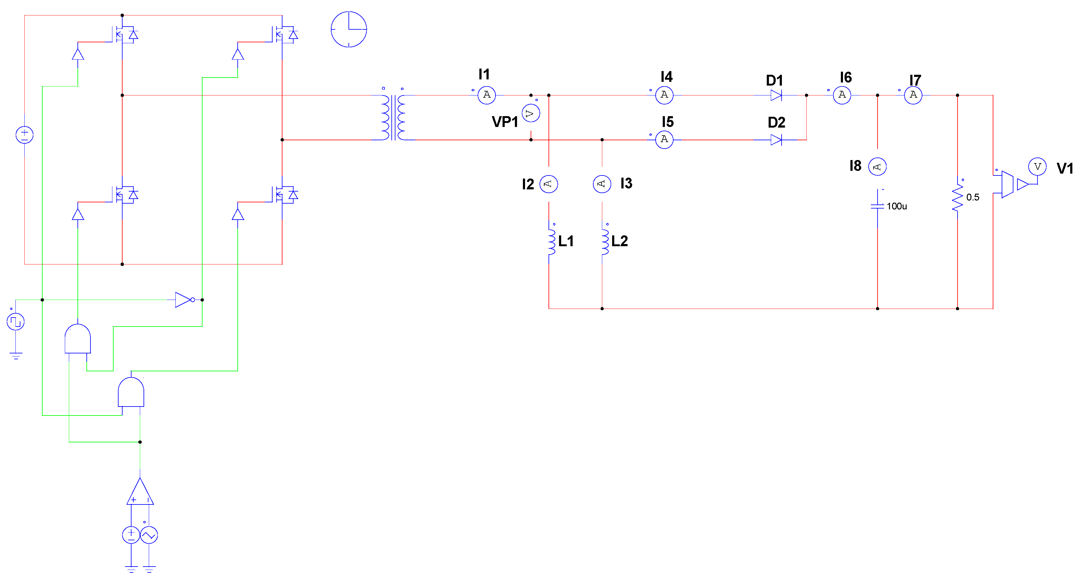
2. Computer Simulation Results
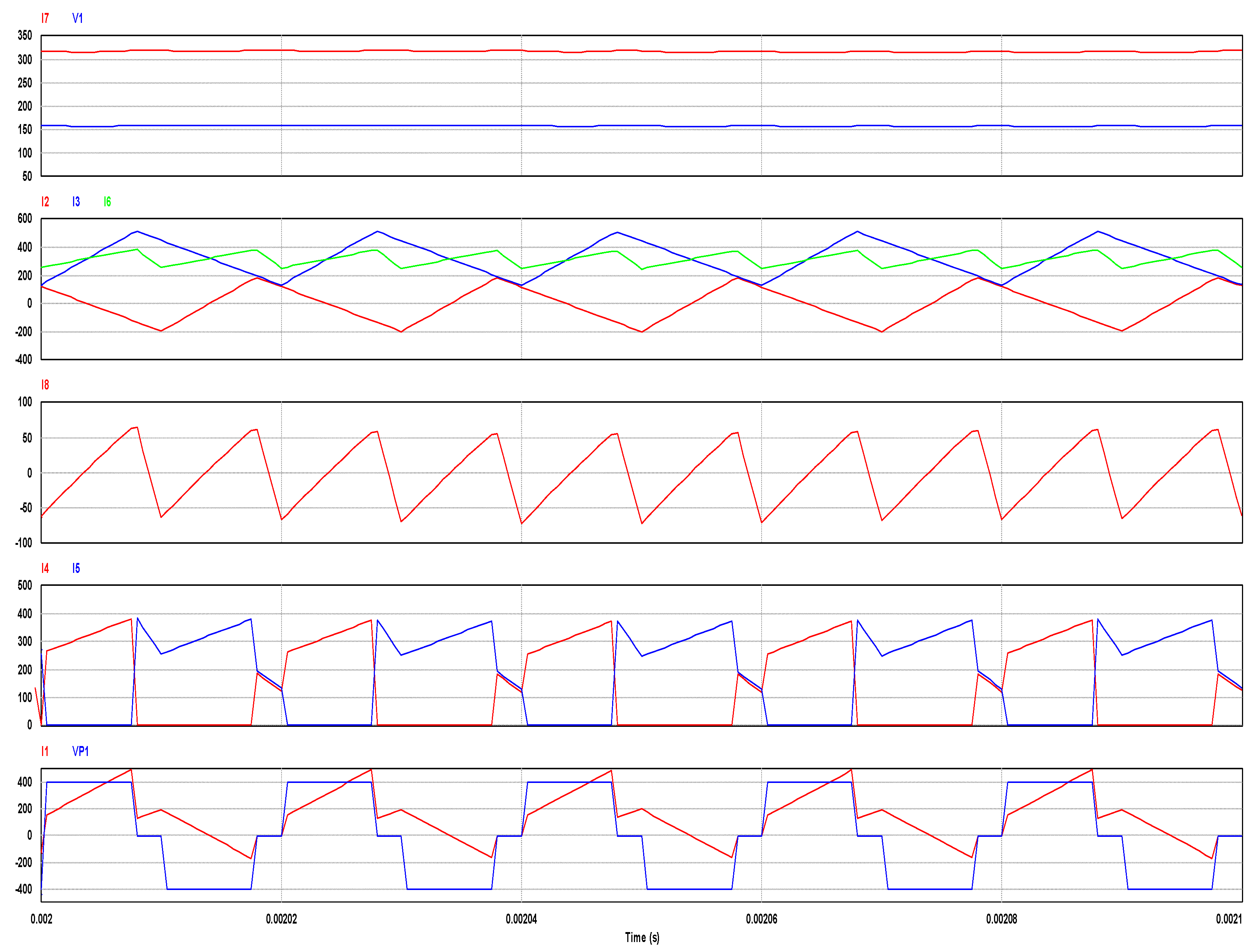
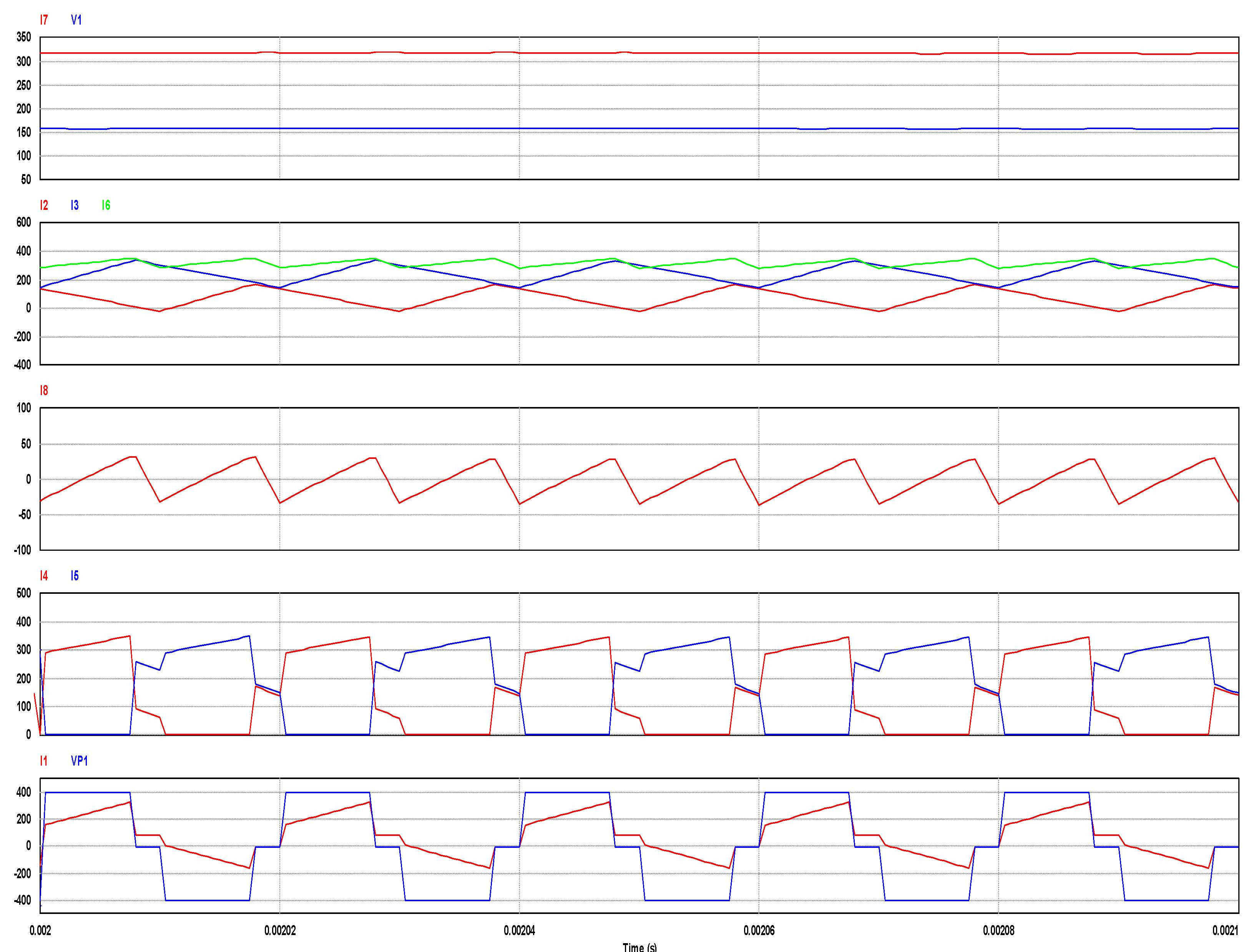
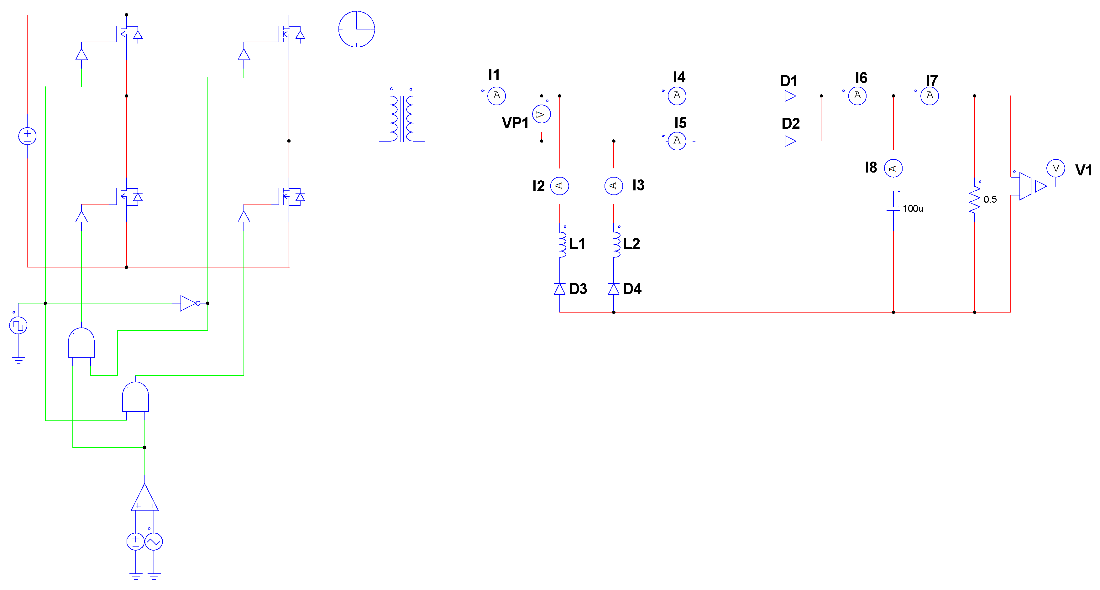
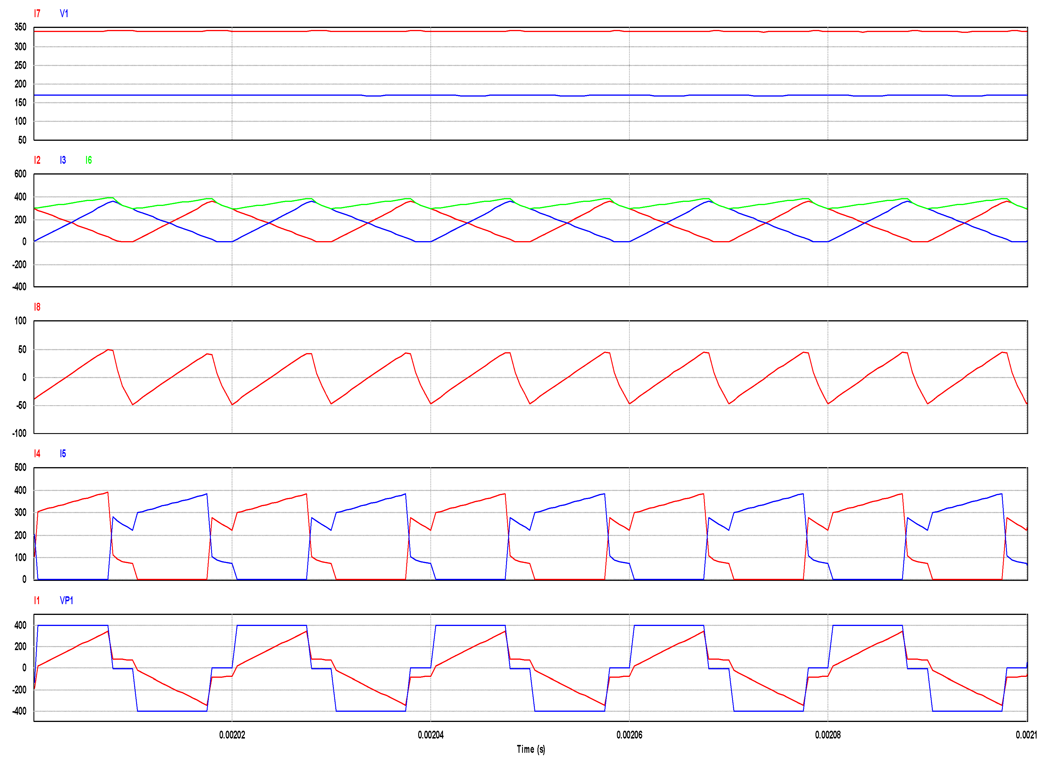
The above-mentioned conclusions about the difference in the average values of the currents through the two inductances, due to the different operating conditions in the first cycle, are confirmed in the present work with the help of a computer simulation diagram done with the PSIM program shown in Figure 2. The observed values are indicated in the diagram and they are shown in Figure 3 and Figure 4 for different inductance values. The units on the ordinate are in volts and amps. The indications of the values shown in the time diagrams are seen in Figure 2, and include the following: I2, I3 (electric currents through the inductances); I1, VP1 (electric current and secondary coil voltage); I4, I5 (electric currents through the diodes); I6 (the sum of I2 and I3); I8 (current through the capacitor); I7, V1 (current and voltage of the load).
The comparison of the results of Figure 3 with those of Figure 4 shows that at a higher inductance value the effect in question is less expressed, i.e., the difference in the values of the average currents through them is smaller. Perhaps this is the reason why researchers did not notice the difference in currents and did not pay attention to the start-up processes.
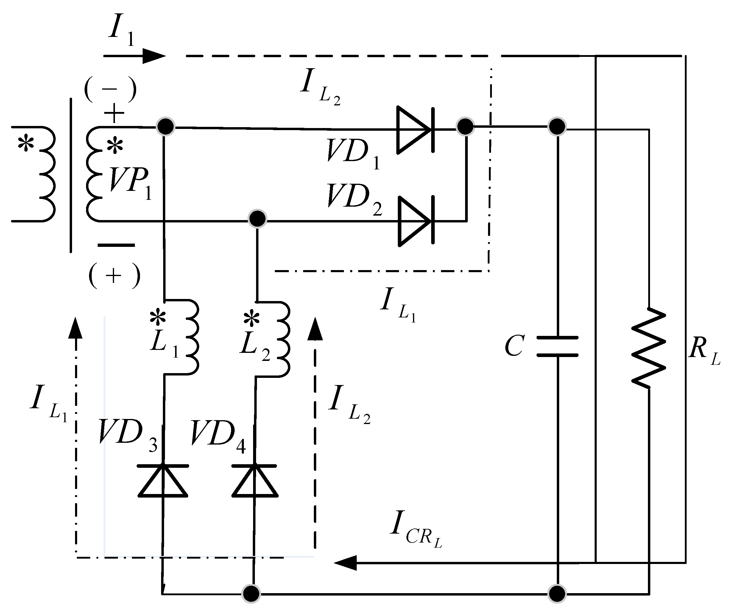
To avoid the asymmetry due to the first operating cycle, this article proposes the successive connection of diodes to inductances, as this circuit is called “Improved Current Doubler Rectifier”, which is shown in Figure 5. It shows that in the first operation cycle at the shown polarity of the voltage of the secondary coil without brackets, electric current flows only through the inductance in the direction of bottom to the top of the diagram. Due to the presence of in this first cycle, there is no current flowing through the inductance . When changing the polarity of the voltage in the second cycle, shown in the figure in brackets, current will flow through the inductance , in the direction of bottom to top. The diagram will have the same results if the first cycle corresponds to the polarity of the voltage shown in brackets. In this way, the circuit becomes symmetrical with respect to the two currents in their first cycle. From the diagram of Figure 5, it is seen that a single-phase bridge rectifier is connected to the secondary coil of the transformer, as the inductances are being connected to cathodes of and . It should be noted that only the asymmetry due to the gradual charging of the capacitor during the startup process remains.
The operation of “Improved Current Doubler Rectifier” is checked with the computer simulation diagram shown in Figure 6. The results are presented in Figure 7 and Figure 8 for the same values of the two inductances corresponding to Figure 3 and Figure 4. Figure 7 and Figure 8 show almost complete symmetry of the circuit in terms of currents through inductances, currents through the diodes, and lack of a direct current component through the secondary coil of the transformer.
3. Experimental Investigation
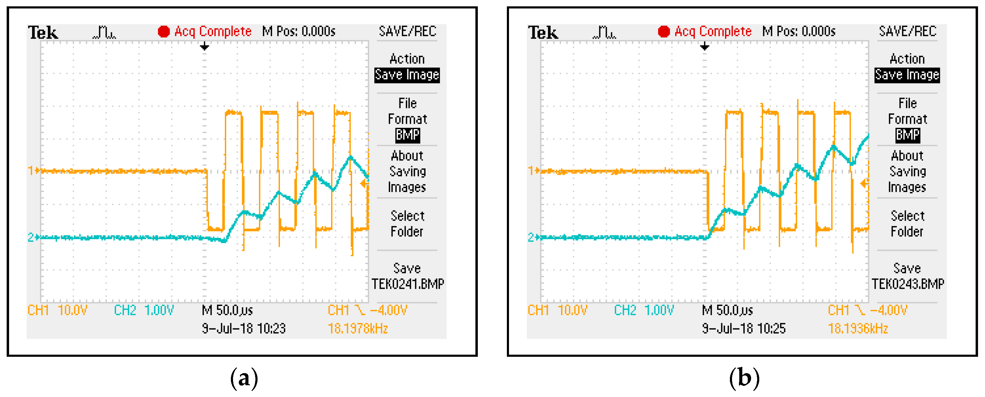
To investigate the start-up processes, a bridge DC/DC converter with a high-frequency transformer has been implemented. This converter is powered by a voltage with a value , obtained after rectification of the voltage of the power supply network. In the converter control system, special measures are provided to ensure the symmetrical operation of the diagonally connected transistors in both half periods. In the first part of the experiment, a standard “Current Doubler Rectifier” of Figure 1 is connected in the secondary side at the inductance value of . The values of the two inductances are specifically selected to be equal, and the measurement is done with an electronic RLC meter. Figure 9 and Figure 10 show oscillograms from the initial run experiment at different time scales. When monitoring the oscillogram of the voltage , the active end of the voltage probe on the oscilloscope’s first channel is connected to the anode of the diode, and the ground, up to the anode of diode . The currents are monitored by a current probe, connected to the second channel at a 100 mV/A scale. The probe is connected so that the positive direction of the current through is from the end to the beginning of each inductance, as the currents and are shown in Figure 5. As all the oscillograms show below, the voltage scale of CH1 is 10 V/div, and the current scale of CH2 is 10 A/div.
From the comparison of Figure 9a,b can be seen the difference in the first operation cycle. At the described connection of the first channel voltage probe, the first cycle corresponds to the negative voltage of the anode to the anode of (therefore positive voltage of anode of to the anode of ). At this first cycle the current through flows in the opposite direction and in the second cycle starts from a negative value that is −2 A. In the first cycle the current through starts from zero value.
From the comparison of Figure 10a,b can be seen the difference in the maximum values of currents during the start-up process. For the inductance , the maximum value is 28 A and for the inductance it is 3 A. Therefore, the difference in the maximum values is 5 A.
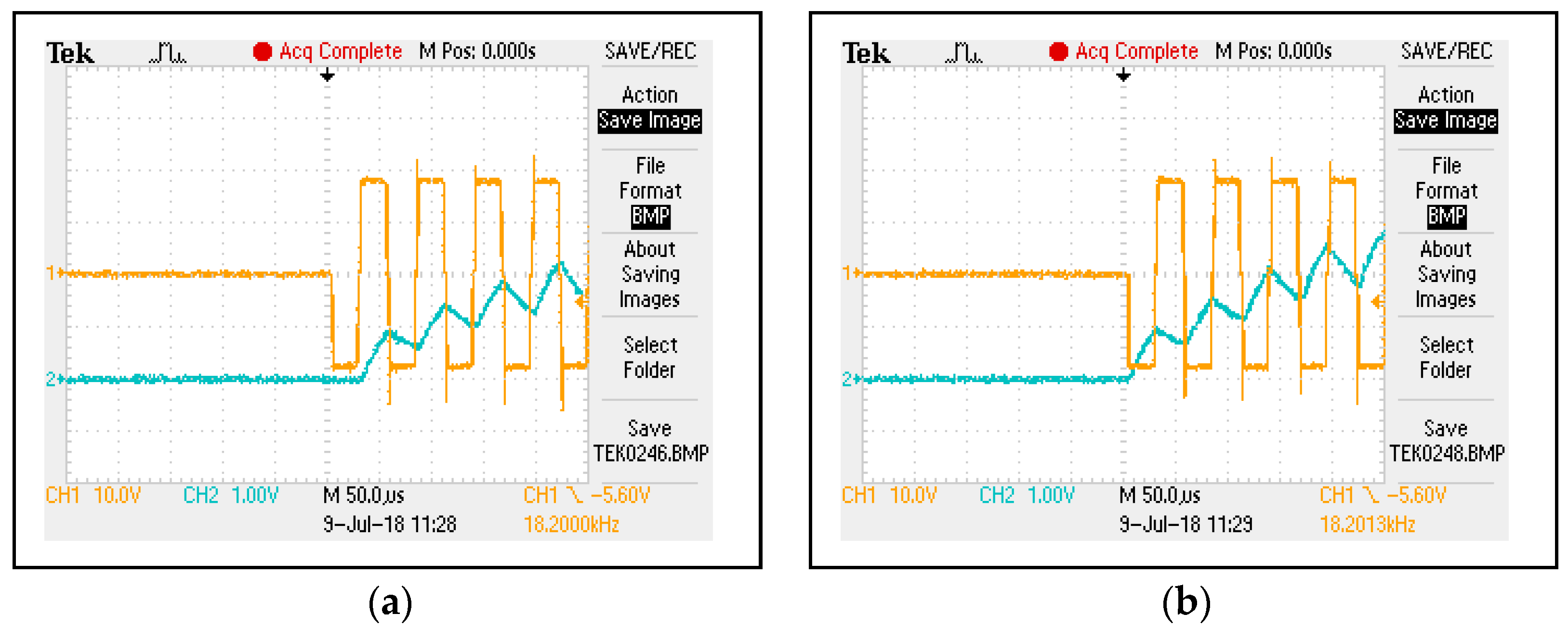
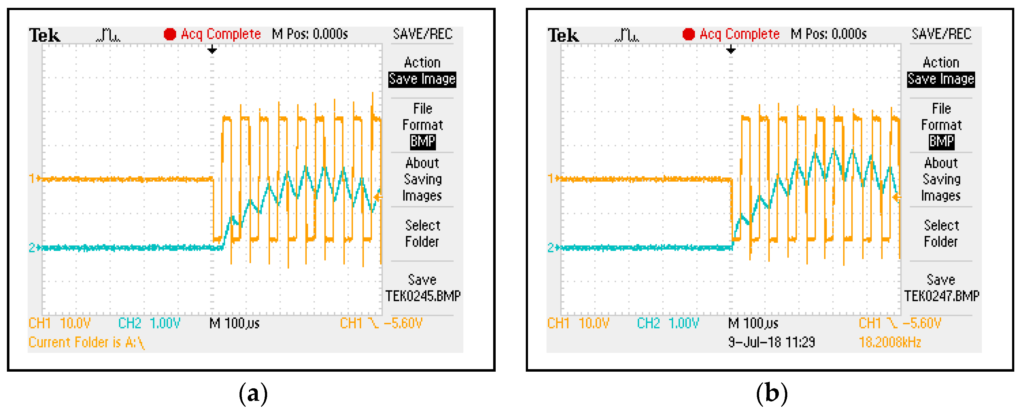
In the second part of the experiment, in the secondary side, is connected the so-called “Improved Current Doubler Rectifier”, which is connected only by adding the two diodes of the anode group in Figure 5, at the same inductance value . Figure 11 and Figure 12 show oscillograms from the start-up processes in different time scales. The position and scale of the voltage and current probes is unchanged.
From the comparison of Figure 11a,b, it is seen that there is no current flowing through the inductance in the opposite direction during the first cycle (unlike Figure 9a). During the second cycle, this current starts at zero value. In the first cycle, the current through starts from a zero value as it is in Figure 9b.
From the comparison of Figure 12a,b, the difference in the maximum current values during the start-up process is visible, for the inductance the maximum value is 24 A and for the inductance , 28 A. Therefore, the difference in the maximum values is 4 A and it is reduced compared to the first case. Although smaller, there is some asymmetry in the currents, due to the gradual increase in capacitor voltage as it was described in the introduction.
4. Conclusions
The results of the researches conducted through computer simulation and those of the experimental studies confirm the original theoretical examination and prove the advantages of the offered solutions in the present work “Improved Current Doubler Rectifier”, which, namely, include the following: improving the symmetry of the currents through the two inductances (at their fully equal values and symmetric control of the converter in the primary side); and the lack of a direct current component in the secondary coil of the transformer. These advantages are achieved by a simple modification of the standard circuit. The advantage, however, is at the expense of a certain disadvantage, i.e., the increased number of “Improved Current Doubler Rectifier” diodes. The proposed circuit could be developed and tested though synchronous current rectification in the secondary side, similar to the “Synchronous current doubler rectifier”.
Funding
This research received no external funding.
Conflicts of Interest
The author declares no conflict of interest.
References
- Balogh, L. The Current-Doubler Rectifier: An Alternative Rectification Technique for Push-Pull and Bridge Converters; Design Note 63; Texas Instruments: Dallas, TX, USA, December 1994; pp. 4-79–4-81. [Google Scholar]
- Mappus, S. PWM IC’s AB Outputs Drive Synchronous Rectifier. Power Electron. Technol. 2003, 2, 52–56. [Google Scholar]
- Texas Instruments. Control Driven Synchronous Rectifiers in Phase Shifted Full Bridge Converters; Application Note SLUA287; Texas Instruments: Dallas, TX, USA, March 2003. [Google Scholar]
- Chiang, B.P.; Hu, M. Switching Analysis of Synchronous Rectifier MOSFET’s with Phase Shifted Full-Bridge Converter and Current Doubler; Application Note 833; Vishay Siliconix: Mansfield, TX, USA, October 2007. [Google Scholar]
- Texas Instruments. Using the UCC3895 in a Direct Control Driven Synchronous Rectifier Applications; User’s Guide SLUU109B; Texas Instruments: Dallas, TX, USA, February 2009. [Google Scholar]
- Garsia, R. ISL6752/54EVAL1Z ZVS DC/DC Power Supply with Synchronous Rectifier User Guide; AN1603; Intersil: Pettas, CA, USA, June 2011. [Google Scholar]
- Wu, T.F.; Tsai, C.; Chang, Y.; Chen, Y. Analysis and Implementation of an Improved Current-Doubler Rectifier with Coupled Inductors. IEEE Trans. Power Electron. 2008, 23, 2681–2693. [Google Scholar]
- Huber, L.; Jovanovic, M.H. Forward-Flyback Converter with Current-Doubler Rectifier with Coupled Inductors: Analysis, Design, and Evaluation Results. IEEE Trans. Power Electron. 1999, 14, 184–192. [Google Scholar] [CrossRef]
- Batarseh, I.; Abu-Quahouq, J.; Mao, H. DC-DC Converter with Coupled-Inductors Current-Doubler. U.S. Patent 6982887B2, 3 January 2006. [Google Scholar]
- Texas Instruments. Current Doubler Rectifier Offers Ripple Cancelation; Application Note SLUA323; Texas Instruments: Dallas, TX, USA, September 2004. [Google Scholar]
- Texas Instruments. UCC3895 Phase Shift PWM Controller EVM Kit Setup and Usage; User Guide SLUU069A; Texas Instruments: Dallas, TX, USA, September 2000. [Google Scholar]
- Lin, B.R.; Huang, K.; Wang, D. Analysis and implementation of full-bridge converter with current doubler rectifier. IEE Proc. Electr. Power Appl. 2005, 152, 1193–1202. [Google Scholar] [CrossRef]
- Renesas Electronics Corporation. ISL 6752/54 EVAL1Z-ZVS DC/DC Power Supply with Synchronous Rectifiers Evaluation Board; AN1603; Renesas Electronics Corporation: Tokyo, Japan, May 2018. [Google Scholar]
- Balogh, L. 100 W, 400 kHz DC/DC Converter with Current Doubler Synchronous Rectification Achives 92% Efficiency; Texas Instruments: Dallas, TX, USA, 2000. [Google Scholar]
- Mao, H.; Yao, L.; Deng, S.; Batarseh, I.; Abdel-Rahman, O.; Liu, J.; Batarseh, I. Inductor Current Sharing of Current Doubler Rectifier in Isolated DC-DC Converters. In Proceedings of the 21st Annual IEEE Applied Power Electronics Conference and Exposition, Dallas, TX, USA, 19–23 March 2006; pp. 770–775. [Google Scholar]
- Song, H.; Zhang, Y.; Zhang, Y. An Improved Current-Doubler Rectifier for the Marine Controlled Source Electromagnetic Transmitter. Math. Probl. Eng. 2018. [Google Scholar] [CrossRef]
- Sun, J.; Webb, K.F.; Mehrotra, V. An Improved Current-Doubler Rectifier with Integrated Magnetics. In Proceedings of the 17th Annual IEEE Applied Power Electronics Conference and Exposition, Dallas, TX, USA, 10–14 March 2002. [Google Scholar] [CrossRef]
- Ruan, X.; Wang, Y. Calculation of the Resonant Capacitor on the Improved Current-Doubler Rectifier ZVS PWM Full-Bridge Converter. IEEE Trans. Ind. Electron. 2004, 51, 518–520. [Google Scholar] [CrossRef]
Figure 1.
Diagram for clarifying the operation in the first cycle.
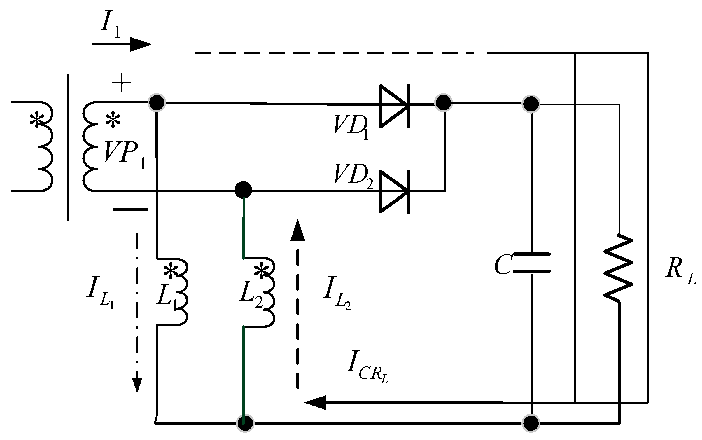
Figure 2.
Computer simulation diagram of the standard “Current Doubler Rectifier”.

Figure 3.
Computer simulation results of a standard “Current Doubler Rectifier” with inductances .

Figure 4.
Computer simulation results of standard “Current Doubler Rectifier” with inductances

Figure 5.
Diagram for clarifying the functioning of “Improved Current Doubler Rectifier”.

Figure 6.
“Improved Current Doubler Rectifier” computer simulation diagram.

Figure 7.
Computer simulation results of “Improved Current Doubler Rectifier” with inductances .

Figure 8.
Computer simulation results of “Improved Current Doubler Rectifier” with inductances

Figure 9.
Horizontal axis scale : (a) voltage –CH1 and current –CH2, (b) voltage –CH1 and current – CH2.
Figure 9.
Horizontal axis scale : (a) voltage –CH1 and current –CH2, (b) voltage –CH1 and current – CH2.

Figure 10.
Horizontal axis scale : (a) voltage –CH1 and current –CH2, (b) voltage –CH1 and current –CH2.
Figure 10.
Horizontal axis scale : (a) voltage –CH1 and current –CH2, (b) voltage –CH1 and current –CH2.
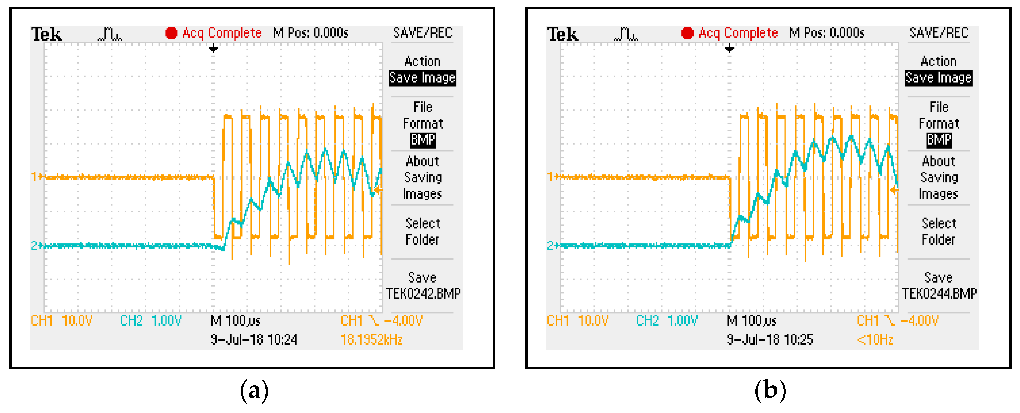
Figure 11.
Scale on horizontal axis : (a) voltage –CH1 and current –CH2, (b) voltage –CH1 and current –CH2.
Figure 11.
Scale on horizontal axis : (a) voltage –CH1 and current –CH2, (b) voltage –CH1 and current –CH2.

Figure 12.
Scale on horizontal axis : (a) voltage –CH1 and current –CH2, (b) voltage –CH1 and current –CH2.
Figure 12.
Scale on horizontal axis : (a) voltage –CH1 and current –CH2, (b) voltage –CH1 and current –CH2.

© 2018 by the author. Licensee MDPI, Basel, Switzerland. This article is an open access article distributed under the terms and conditions of the Creative Commons Attribution (CC BY) license (http://creativecommons.org/licenses/by/4.0/).
Share and Cite
MDPI and ACS Style
Antchev, M. Improved Current Doubler Rectifier. Energies 2018, 11, 2485. https://doi.org/10.3390/en11092485
AMA Style
Antchev M. Improved Current Doubler Rectifier. Energies. 2018; 11(9):2485. https://doi.org/10.3390/en11092485
Chicago/Turabian StyleAntchev, Mihail. 2018. "Improved Current Doubler Rectifier" Energies 11, no. 9: 2485. https://doi.org/10.3390/en11092485
APA StyleAntchev, M. (2018). Improved Current Doubler Rectifier. Energies, 11(9), 2485. https://doi.org/10.3390/en11092485
Note that from the first issue of 2016, this journal uses article numbers instead of page numbers. See further details here.