Integrated Solution for Driving Series-Connected IGBTs and Its Natural Intrinsic Balancing

1
Graduate Program in Electrical Engineering, Universidade Federal de Minas Gerais, Av. Antônio Carlos 6627, Belo Horizonte MG 31270-901, Brazil
2
Department of Electronic Engineering, Universidade Federal de Minas Gerais, Av. Antônio Carlos 6627, Belo Horizonte MG 31270-901, Brazil
*
Author to whom correspondence should be addressed.
Energies 2019, 12(12), 2406; https://doi.org/10.3390/en12122406
Submission received: 7 May 2019
/
Revised: 17 June 2019
/
Accepted: 20 June 2019
/
Published: 22 June 2019
(This article belongs to the Special Issue Analysis, Design and Modeling of Modular Power Converters)
Abstract
:The use of series connected IGBTs is still a current subject in literature, despite such a discussion having started in the 1990s. Though countless academic studies, there are currently no available commercial products on the market for medium voltage inverters (up to 4.16 kV) and lower power (up to 1 MW) using this technology. This is related to the difficulty of ensuring the dynamic and static voltage sharing between IGBTs, giving rise to relatively expensive and complex firing circuits, when compared to the components they intend to control. Therefore, this article aims to present a simple and low-cost alternative, still effective for driving low voltage series-connected IGBTs, specifically for the encapsulation TO-247 type. Experimental results are presented showing the behavior of the solution under several operating conditions.
Keywords:
association; series; IGBTs; TO-247; thyristors; circuit; firing; inverter; medium; voltage1. Introduction
The medium voltage semiconductor device market is fairly restricted and has a low component consumption when compared to the low voltage semiconductors market. Thus, the speed of development and the cost of medium voltage semiconductor devices has not followed the same trend seen in the low voltage device market over the last few decades.
This deflection between the evolutionary curve of these two areas creates the opportunity to review methods and topologies that address the use of series-connected semiconductor devices. With specific interest in the niche of medium voltage inverters (up to 4.16 kV) with lower power (up to 1 MW), more efficient, advanced and lower cost components, currently available on the low voltage market, can be used in series connection, in order to meet the requirements of medium voltage equipment. However, this better trade-off collides with the difficulty of ensuring the dynamic and static voltage sharing between the devices.
Some IGBTs series connection techniques were introduced and discussed in [1,2,3,4], which summarized that the difficulties of this association were related to the following intrinsic characteristic differences in: Leakage currents (Ices); tail currents; output capacitances (Cce); gate threshold voltages (Vth); gate-emitter capacitances (Cge). As well as the following extrinsic characteristics, referring to the load and gate circuit differences in: Series parasitic inductances between devices; control circuits, due time delays between parallel firing channels; parasitic capacitances of each gate driver power supply.
There are many methods that aim to overcome such differences and ensure voltage sharing. Primarily, they can be divided into three broad categories and some subcategories [5]: Passive or active snubbers circuits; active gate control circuits; and voltage clamping circuits. As shown in Figure 1.
The static voltage unbalance is caused by the difference in the device tail current, resulting in distinct widths of their depletion regions and voltage blocking. In order to make it clear, a practical turn-off switching example, obtained by [4], is presented at Figure 2a and it shows the static voltage unbalance occurring before 35 µs (turn-on) and after 65 µs (turn-off) instants. This physical effect is usually avoided by a parallel resistor with each device in series. In this regard, they can also be used together with active methods, as these usually act only during switching transients [6,7,8]. Also, they can be series-connected with zener diodes [9,10,11], reducing losses by limiting their operation range. In the active category, there are methods that temporarily put the device back into the active region, increasing the losses of the semiconductor devices. For example, the active voltage control (AVC) [12,13] provides a temporary clamping preconditioning step, avoiding the static unbalance after a certain period, under penalty of a complex analog and digital control system. Also, there is a zener voltage clamp feeding the gate signal back [3,14], which limits the static voltage unbalance between devices. However, this would not necessarily reach parity, because it fits more adequately as a maximum voltage protection or an active clamping.
The dynamic voltage unbalance is the one which occurs during the switching transient, and can essentially be rejected in two ways [7]. The first one is the load-side balancing and uses simple circuits such as passive snubbers C, RC, RCD, PC [5,10] or more complex circuits such as active snubbers [15,16]; The other is the gate-side balancing, where the firing circuit is used to actively act on the current or voltage profile of the gate. Also, for practical elucidation, a turn-on transient example [4], is presented in Figure 2b where a voltage zoom shows clearly a poor dynamic voltage sharing when no-balancing method is applied.
In [1], an active firing solution for series-connected IGBTs was described and an analogue feedback control circuit was used. Thus, the individual firing circuits received a predefined reference and manipulated each gate voltage profile, so that the Vce voltages of the devices followed the reference. However, by restricting the transient, imposing a slower reference, and by defining a fixed initial preconditioning stage, this method increases the switching losses [5]. In [17], a current feedback control (di/dt) was internally inserted to the previous Vce voltage controller, being able to increase its bandwidth, under the penalty of inserting a new sensor and making the control adjustment more complex. Another evolution of the method [1] was proposed by [8], where the fixed parameters of the model (Vce reference and preconditioning step) were now dynamically estimated and varied in order to obtain optimal losses and voltage sharing. However, the greater flexibility imposes the need for a micro controlled system with A/D conversion, making it even more complex and with dynamic limitation.
In [18], the voltage unbalance was avoided by inserting time delays into the gate signals of each semiconductor device. Effectively, in a series connection, leading or lagging one device firing command directly influences the blocking voltage of the others. For that purpose, a feedback control system tracks the required delays to impose optimal balancing, taking some time up to the convergence. In general, the solution presented low reliability [5], besides the need for micro-processing and A/D conversion, which greatly increased its complexity and reduced its dynamic response. Therefore, it ended up limiting the class of IGBTs in which such a system could be used, being restricted to those with slower switching times. In [19], a micro-controller was used to track and reject delay times in the IGBT firing commands, as well as to integrate the concepts of passive control (snubber RC) and active voltage clamping.
In [20], to overcome the asynchronous firing commands, a balancing core was proposed (Figure 3), avoiding time differences of the firing commands due to the imposition of magnetically induced currents in the gate driver circuits. According to [5], this method presents moderate reliability and high complexity, due to the need for parallel coupling between the firing channels.
Returning to the concept of passive voltage sharing, in [21] the effects of the parasitic capacitances on the series connected IGBTs were analyzed. They came from the gate driver power supply and were due to the load side geometry. Two proposals were presented: The first was based on a self-powered firing circuit, which decreased its parasitic capacitance; the second one was based on a three-dimensional connection of the IGBTs, which physically also allowed for the decrease and more balanced distribution of parasitic capacitances. Essentially, this method explored the need for a careful look at one of the extrinsic characteristics. In this way, interestingly, it focused on the cause and not on its effect. However, the intrinsic characteristics were totally denied.
An interesting firing solution was proposed in [22] for individual IGBT firing. It used a double magnetic link through which the power supply energy and the firing command (high-frequency encoded) were transmitted (Figure 4). Therefore, it is possible to eliminate the auxiliary power supplies required for each gate driver circuit. However, high-frequency data transmission, over a non-insulated link from the load side, makes this method more complex to ensure electromagnetic compatibility and the ability to decode the firing signal.
Based on the literature reviewed, it is clear that the complex methods are suitable for firing medium voltage IGBTs, as they present a dynamic response limitation. They demonstrate results for devices with switching times of a few micro-seconds. In addition, its complexity drastically increases the cost, due to the use of digital and/or analogue feedback systems, besides the need for auxiliary power supplies with specific galvanic isolation for medium voltage class. Therefore, they are only justified when driving medium voltage and high power IGBTs, since it equalizes its relative cost. Consequently, they would give rise to solutions with tens of kilovolts.
This article specifically focused on practical feasibility and proposes an effective, simple and low-cost solution oriented to the specific niche of medium voltage inverters (up to 4.16 kV) with lower power (up to 1 MW). In this regard, it is considered that the use of semiconductor devices will be restricted to ultra-fast IGBTs (for example, with rise times less than 100 ns), with a forward blocking voltage of 1200 V and manufactured with the encapsulation TO-247. These devices cost about eight dollars, representing real restriction in the complexity of the firing system and, therefore, in its cost, since it is supposed to be cheaper or in the same price range of the power device it intends to command. In this sense, an optimized power layout and gate driver circuit was proposed based on the typical command of thyristors using pulse transformers. A synchronous rectifier was galvanic isolated by a pulse transformer and it was responsible for treating the firing current pulses, as well as controlling the gate´s maximum and minimum voltage. These commands were imposed via two primary simple magnetic loops—one for positive and another for negative commands. Both were driven by a pulse amplifier, as shown in Figure 5.
2. Main Requirements
A. Perfect Firing Sync
One of the main factors of voltage unbalance during the switching transient of series-connected IGBTs is caused by time delays, due to individualized parallel channels for firing the devices. Considering the use of ultra-fast IGBTs with switching times of tens of nanoseconds, even a small uncertainty in the timing accuracy of firing channels can lead to the voltage unbalance. Thus, it is indispensable to propose a firing system capable of imposing an extremely precise synchronism in the gate command of each series-connected semiconductor device.
B. Power and Control Galvanic Insulation
In the matter of series connected devices for a medium voltage multilevel application, another important issue is how to provide galvanic insulated firing circuits among devices and the controller. Usually, galvanic isolation is done through small individual transformers. Its insulation level is crucial to a medium voltage application, which increases its cost and size.
On the other hand, in the vast majority, the insulation of the command circuits is done through optical transmitters and receivers. However, the cost of these receivers, transmitters and the optical fibers is also a limiting factor in their use. This restricts their application to higher power and voltage systems where their relative cost is reduced.
C. Relative Cost
Especially in this paper, the cost factor imposes strict limits, after all, the value of a gate driver should be lower than or equal to the device it intends to control. Therefore, when considering only IGBTs with encapsulation TO-247, simplicity becomes indispensable for project viability. Thus, extrinsic and intrinsic causes must first be attacked, as opposed to the direct attempt to reject its effects, since this would imply a higher cost for the solution.
D. Extrinsic Characteristics
Regarding the extrinsic issues, the concern with electrical parasitic characteristics is very important. They are derived from the mechanical and electrical design, as evidenced in [21], regarding the parasitic capacitance of the power supplies. Therefore, a precise symmetry of the control and power circuits must be imposed. Also, magnetic loops induced by high current variations must be avoided in the firing circuits.
E. Intrinsic Characteristics
Regarding the nature of the intrinsic characteristics, it is important to carefully select the IGBT models, since fabrication technologies influence the physical behavioral effects of the series connection [23]. Certain physical effects naturally tend to bring the devices to share voltage during switching transients, such as the Miller effect [24,25]. Where, the fastest devices “slow down”, while the slower ones “accelerate” during the transient. Such behavior is a consequence of the inverse proportional characteristic of the gate-collector capacitance (Cgc) in relation to the collector-emitter voltage (Vce).
F. Passive Balancing
Also, to avoid any intrinsic differences, passive snubbers with smaller percentage values should be used, so far as the unbalance is naturally reduced from the point of view that the solution is optimized, primarily, for causes and, secondarily, for the effects.
3. Gate Driver
Analyzing the previous section, the proposed firing solution aimed to comply with requirements A, B and C. As shown in Figure 5, two simple primary magnetic loops were responsible for both power energy and firing command (typical thyristor concept). Therefore, there was no need for a power supply for each IGBT or individual optical fibers control, which made the cost of the control system less dependent on the number of serial devices. However, for the IGBTs, the gate voltage must be kept constant after turn-on and turn-off. Thus, the individual gate driver circuits were supplied by two types of periodic positive or negative current pulses (the refreshing and switching pulses—see Figure 6). Benefiting from the IGBT gate storage function [26] and the very small parasitic capacitance of the gate-driver components, the gate-emitter capacitance (Cge) can be easily charged, discharged or kept constant when clamped positive or negatively by zener diodes, setting the gate voltage levels for turn-on and off (Figure 6).
In more detail, Figure 7 shows the push-pull pulse amplifier circuit that was supplied by 30–60Vdc and had a 30 V freewheel zener diode; the double primary pulse transformers with turns ratio of 1:1:7; the individual gate driver circuits implemented by two 6.5 V small zener diodes used for triggering the mosfets type N and P; two 18.5 V zener diodes responsible for setting the gate voltage levels for turn-on and off; and the RS and RC snubbers for n series-connected IGBTs.
The solution presented imposed an extremely precise synchronism, since only one command channel was responsible for firing or blocking, simultaneously, all devices in series. In addition, when using toroidal cores (Figure 5) and wires with medium voltage insulation, the necessary galvanic isolation was obtained between power and control. Therefore, requirements A and B were fulfilled. Requirement C was achieved as a consequence of simplicity, since the method did not use complex microprocessor systems, extra sensors, A/D converters and feedback controllers. In addition, the gate driver circuit was designed by shelf components, allied to the fact that it was a method that was less dependent from the number of devices.
4. Hexagonal Sub-Module
As previously defined, the extrinsic characteristics refer to the power and control circuit. The use of IGBTs with encapsulation TO-247 facilitated its integration using printed circuit boards. Thus, the mechanical design of the power and control could be fully integrated in order to minimize the inductances, parasitic capacitances and magnetic loops that could be induced by the high current variations during switching transients. Jointly, it is indispensable to have a mechanical and electrical design totally symmetrical between the series-connected devices. In this regard, in order to comply with the aforementioned requirement D, Figure 8 shows a developed model that was a hexagonal sub-module concept with six series-connected IGBTs. It is responsible for one of the voltage levels in a larger three-dimensional multilevel converter structure, which is not the subject of this article.
5. Natural Intrinsic Balancing
It is very important to use IGBT families whose technologies maximize physical effects that lead to natural voltage sharing. In this case, IGBT IKQ75N120CH3, manufactured by Infineon was used. It is based on Highspeed3 technology, a vertical structure with a trench gate and field stop layer [27]. Figure 9 shows two physical effects, present in this family, where only a little is known, but is unprecedented in the series connection context. The first effect is called self-turn-on [28,29], identified by the increasing of the gate voltage rise between instants −20 ns to 0 ns. The second effect is called negative gate capacitance [30,31], which is identified by the gate voltage drop between 0 ns and 60 ns.
To verify the natural intrinsic balancing, a turn-on experiment was carried out with three different forward blocking voltages (0 V, 100 V and 200 V) and no-load current, shown in Figure 9. In this way, it could be seen that one IGBT with a higher forward blocking voltage presented its gate command leading and with larger amplitude than the other one with a smaller forward blocking voltage. This behavior was reversed by the negative gate capacitance effect at the final switching instants (between 50 ns and 100 ns), lagging the command to re-equalize the gate-emitter voltage back again (the arrows indicate the leading and lagging effects). Therefore, a negative physical feedback was present in the gate signal, which led to the increase or decrease of the switching times and, naturally, imposed the voltage sharing of the series-connected devices.
In addition to the behavioral analysis defined in requirement E, passive snubbers were still necessary to avoid physical differences during the tail current period (requirement F). No technique is simpler, more effective and popular than the use of passive snubber circuits. Its use increases total losses, but it has the trade-off presented by the reduction of the power device switching losses [5]. A comparison of several passive snubbers C, RC, RCD and PC is made in [10], which was focused on series association. However, it did not present major improvements, as the slightly better results come with an increased circuit complexity.
Therefore, we started with the simplest snubber circuit possible, consisting of a resistor (Rs) and a RC filter (Figure 7).
6. Experimental Results
6.1. Test Bench and Hexagonal Sub-Module
A test bench was assembled according to the power scheme shown in Figure 10, consisting of two hexagonal sub-modules, output inductor, dual secondary transformer and a 12-pulse rectifier feeding a DC link with nominal voltage of 1200 V.
Figure 11 shows pictures of the hexagonal power sub-module. In its top view, we can see the six sets of IGBTs, the individual gate driver circuits, powered by pulse transformers designed with toroidal cores, as well as the two primary isolated loops responsible for the positive and negative gate current pulses. In the bottom view, the snubbers circuits can be seen.
All experiments presented below show many waveforms since, in general, they are comparisons between the six series-connected IGBTs. Due to the impossibility of obtaining six simultaneous measurements, a variable was used to synchronize the experiments carried out separately. Therefore, they could be seen under the same time base, imposing temporal determinism over their comparisons. For this, nothing was fairer than the use of the primary current firing pulse that is shared by all semiconductor devices in the series string. In this sense, the experiments were always repeated six times, obtaining the temporal sync signal and the measured variable of interest for each device. Subsequently, the experiments were arranged together, where the sync signals were the time reference for positioning the signals of interest.
6.2. Gate Command Synchronization
Figure 12 shows the operation of the control firing system for switching under zero forward blocking voltage. As expected, perfect synchronization between all gate-emitter voltages was obtained. Yet, the primary current firing pulses were shown in order to prove the temporal determinism of the results.
6.3. Natural Intrinsic Balancing without Snubber
Figure 13 and Figure 14 show a turn-on and a turn-off transient switching, respectively. They were performed with a current of 60 A, total voltage of 1200 V and in the snubberless condition, to avoid any influence on the Vce voltages. The Vce and Vge voltages of the six series-connected IGBTs are shown, as well as the collector current (Ic). The new results corroborate with the argument cited in topic 5, since the fastest device (IGBT 6+) is clearly the one with the slowest and lowest amplitude gate voltage (see arrows). Especially, for the case of the turn-off switching (Figure 14), the most apparent effects were the Miller effect and the negative gate capacitance. Therefore, in both cases, turn-on or turn-off, a negative feedback on the gate signal was present, which led to the intrinsic natural balancing during transients.
6.4. Final Results with Static Analysis
In this topic, the complete solution, using the snubbers circuits, has been experimented for different current conditions (0 A, 30 A and 60 A) and under same 1200 V total blocking voltage. In these experiments, unlike the previous analysis, static imbalances are also considered.
Figure 15 shows the turn-on switching with no-load current; however, it is possible to verify the snubbers circuits current (of negative side devices—Figure 10). The result shows a perfect balancing during the static and dynamic periods.
Figure 16 and Figure 17 show the turn-on switching with 30 A and 60 A load currents, respectively. There is a maximization of the physical effects, responsible for the natural intrinsic balancing, in the attempt to reject the unbalances caused by the increased collector current. The results demonstrated an effective dynamic balancing, even under a critical condition, since the transient switching time was about 60 ns. In addition, there was also a tendency to increase the static differences in the collector-emitter voltages as the current increased. However, snubber circuits fulfill their role in keeping these differences within a threshold that does not greatly affect transient behavior, as obtained.
Figure 18 and Figure 19 show the turn-off switching with 30 A and 60 A load currents, respectively. Again, a maximization of the physical effects, responsible for the natural intrinsic balancing, is inferred with the increase of the collector current, resulting in an optimal dynamic voltage sharing. There is also an increase in static differences among collector-emitter voltages due the current increase, as can be noticed during the off-state. Clearly, some physical behaviors are current dependent as, for instance, the space charge region width [32,33], leading to greater differences on the blocking voltage when compared with a no-load turn-off. It means that increasing intrinsic physical differences will result in a slightly greater static voltage unbalance, since its limitation is imposed only by passive snubbers during the off-state (refer to Figure 17 that shows satisfactory dynamic results during the turn-on, despite of the initial static voltage unbalance caused by a previous turn-off switching).
7. Conclusions
Under a holistic view on the practical feasibility of the series-connected low voltage IGBTs, this article presented an integrated solution based on an optimized power design and a simple and low-cost gate firing solution. The extrinsic and intrinsic voltage unbalancing causes were discussed and they must first be attacked, as opposed to the direct attempt to reject their effects. In addition, the natural intrinsic balancing concept was introduced along with the importance of selecting IGBT families whose technologies maximize the physical behaviors that are helpful for voltage sharing. In this sense the results prove that the integrated solution under the proposed requirements was feasible, efficient and low cost, being able to impose static and dynamic voltage sharing among the series-connected IGBTs. Thus, this solution may be the basis for the development of a new class of medium voltage multilevel converters. A class that, by leveraging the low-voltage IGBTs series association can take advantage of its improved performance, higher frequency switching capabilities, easy mounting on printed circuit boards, its inherent application in multi-level topologies, in addition to its extremely low cost. As a matter of fact, these are the positive factors supporting the studies presented here.
Author Contributions
Conceptualization, G.O.F.; methodology, G.O.F.; validation, G.O.F.; formal analysis, G.O.F.; investigation, G.O.F.; resources, G.O.F., P.C.C. and M.A.S.M.; data curation, G.O.F.; writing—original draft preparation, G.O.F.; writing—review and editing, M.A.S.M. and P.C.C.; visualization, P.C.C. and M.A.S.M.; validation, P.C.C. and M.A.S.M.; supervision, P.C.C. and M.A.S.M.
Funding
This research received no external funding.
Acknowledgments
The authors thank the Power Electronics Group (GEP) and the Graduate Program in Electrical Engineering of Universidade Federal de Minas Gerais, for their collaboration on this paper.
Conflicts of Interest
The authors declare no conflicts of interest.
References
- Palmer, P.R.; Githiari, A.N. The series connection of IGBTs with optimized voltage sharing in the switching transient. In Proceedings of the Power Electronics Specialists Conference, PESC’95, Atlanta, GA, USA, 18–22 June 1995; Volume 1, pp. 44–49. [Google Scholar]
- Hong, S.; Chitta, V.; Torrey, D.A. Series connection of IGBT’s with active voltage balancing. IEEE Trans. Ind. Appl. 1999, 35, 917–923. [Google Scholar] [CrossRef]
- Bruckmann, M.; Sommer, R.; Fasching, M.; Sigg, J. Series connection of high voltage IGBT modules. In Proceedings of the Industry Applications Conference, Third IAS Annual Meeting, St. Louis, MO, USA, 12–15 October 1998; Volume 2, pp. 1067–1072. [Google Scholar]
- Palmer, P.R.; Rajamani, H.S.; Dutton, N. Experimental comparison of methods of employing IGBTs connected in series. Proc. Electr. Power Appl. IEEE 2004, 151, 576–582. [Google Scholar] [CrossRef]
- Shammas, N.Y.A.; Withanage, R.; Chamund, D. Review of series and parallel connection of IGBTs. IEE Proc. Circuits Devices Syst. 2006, 153, 34–39. [Google Scholar] [CrossRef]
- Hong, S.; Lee, Y.G. Active gate control strategy of series connected IGBTs for high power PWM inverter. In Proceedings of the IEEE 1999 International Conference on Power Electronics and Drive Systems, Hong Kong, China, 27–29 July 1999; pp. 646–652. [Google Scholar]
- Abbate, C.; Busatto, G.; Lannuzzo, F. High-voltage, high-performance switch using series-connected IGBTs. IEEE Trans. Power Electron. 2010, 25, 2450–2459. [Google Scholar] [CrossRef]
- Lim, T.C.; Williams, B.W.; Finney, S.J.; Palmer, P.R. Series-connected IGBTs using active voltage control technique. IEEE Trans. Power Electron. 2013, 28, 4083–4103. [Google Scholar] [CrossRef]
- Mazuela, M.; Baraia, I.; Sanchez, A.R.; Echeverria, I.; Torre, I.; Atutxa, I. Simple Voltage Balancing Method to Protect Series-Connected Devices Experimentally Verified in a 5L-MPC Converter. IEEE Trans. Ind. Electron. 2018, 65, 3699–3707. [Google Scholar] [CrossRef]
- Zhang, F.; Yang, X.; Ren, Y.; Feng, L.; Chen, W.; Pei, Y. A hybrid active gate drive for switching loss reduction and voltage balancing of series-connected IGBTs. IEEE Trans. Power Electron. 2017, 32, 7469–7481. [Google Scholar] [CrossRef]
- Baraia, I.; Barrena, J.A.; Abad, G.; Segade, J.M.C.; Iraola, U. An experimentally verified active gate control method for the series connection of IGBT/diodes. IEEE Trans. Power Electron. 2012, 27, 1025–1038. [Google Scholar] [CrossRef]
- Yang, X.; Zhang, J.; He, W.; Long, Z.; Palmer, P.R. Physical investigation into effective voltage balancing by temporary clamp technique for the series connection of IGBTs. IEEE Trans. Power Electron. 2018, 33, 248–258. [Google Scholar] [CrossRef]
- Zhang, J.; Palmer, P.; Zhang, X.; He, W. Analysis of an effective voltage sharing method for IGBTs connected in series. In Proceedings of the IECON 2014—40th Annual Conference of the Industrial Electronics Society, Dallas, TX, USA, 29 October–1 November 2014; pp. 1261–1269. [Google Scholar]
- Piazzesi, A.; Meysenc, L. Series connection of 3.3 kV IGBTs with active voltage balancing. In Proceedings of the IEEE 35th Annual Power Electronics Specialists Conference, Aachen, Germany, 20–25 June 2004; Volume 2, pp. 893–898. [Google Scholar]
- Lim, T.C.; Williams, B.W.; Finney, S.J. Active snubber energy recovery circuit for series-connected IGBTs. IEEE Trans. Power Electron. 2011, 26, 1879–1889. [Google Scholar] [CrossRef]
- Yang, L.; Fu, P.; Yao, X.; Wang, J. A module based self-balanced series connection for IGBT. In Proceedings of the Energy Conversion Congress and Exposition, Pittsburgh, PA, USA, 14–18 September 2014; pp. 1953–1958. [Google Scholar]
- Wang, Y.; Khaizaran, M.A.; Palmer, P.R. Controlled switching of high voltage IGBTs in series. In Proceedings of the IEEE Conference on Electron Devices and Solid-State Circuits, Hongkong, China, 16–18 December 2003; pp. 297–300. [Google Scholar]
- Gerster, C. Fast high-power/high-voltage switch using series-connected IGBTs with active gate-controlled voltage-balancing. In Proceedings of the Applied Power IEEE Electronics Conference and Exposition, Orlando, FL, USA, 13–17 February1994; pp. 469–472. [Google Scholar]
- Ji, S.; Lu, T.; Zhao, Z.; Yu, H.; Yuan, L. Series-connected HV-IGBTs using active voltage balancing control with status feedback circuit. IEEE Trans. Power Electron. 2015, 30, 4165–4174. [Google Scholar] [CrossRef]
- Abe, Y.; Maruyama, K. Multi-series connection of high-voltage IGBTs. Fugi Electr. J. 2002, 75, 1–4. [Google Scholar]
- Nguyen, T.; Jeannin, P.O.; Vagnon, E.; Frey, D.; Crebier, J.C. Series connection of IGBT. In Proceedings of the Applied Power Electronics Conference and Exposition (APEC), Palm Springs, CA, USA, 21–25 February 2010; pp. 2238–2244. [Google Scholar]
- Brehaut, S.; Costa, F. Gate driving of high power IGBT through a Double Galvanic Insulation Transformer. In Proceedings of the IEEE Industrial Electronics, IECON 2006–32nd Annual Conference, Paris, France, 7–10 November 2006; pp. 2505–2510. [Google Scholar]
- Palmer, P.R.; Githiari, A.N.; Leedham, R.J. A comparison of IGBT technologies for use in the series connection. In Proceedings of the Power Electronics and Variable Speed Drives Conference, Nottingham, UK, 23–25 September 1996; pp. 236–241. [Google Scholar]
- Consoli, A.; Musumeci, S.; Oriti, G.; Testa, A. Active voltage balancement of series connected IGBTs. In Proceedings of the Industry Applications Conference Thirtieth IAS Annual Meeting, Orlando, FL, USA, 8–12 October 1994; Volume 3, pp. 2752–2758. [Google Scholar]
- Hess, H.L.; Baker, R.J. Transformer less capacitive coupling of gate signals for series operation of power MOS devices. IEEE Trans. Power Electron. 2000, 15, 923–930. [Google Scholar] [CrossRef]
- Maurice, B.; Wuidart, L. Drive Circuits for Power MOSFETs and IGBTs. ST Microelectronics Application Notes. Available online: https://www.st.com (accessed on 10 February 2019).
- Chiola, D.; Husklen, H. 1200 V High Speed 3: IGBT A New IGBT Family Optimized for High-Switching Speed. AN-IGBT-09-2013-V1.1-EN-019. Available online: https://www.infineon.com/ (accessed on 15 March 2019).
- Münster, P.; Schräder, R.; Tran, Q.T.; Gierschner, S.; Eckel, H.G. Influence of gate structures and electrical boundary conditions on self-turn-on of HV IGBTs. In Proceedings of the 19th European Conference on Power Electronics and Applications, Warsaw, Poland, 11–14 September 2017. [Google Scholar]
- Feng, H.; Yang, W.; Onozawa, Y.; Yoshimura, T.; Tamenori, A.; Sin, J.K. Transient turn-on characteristics of the fin p-body IGBT. IEEE Trans. Electron Devices 2015, 62, 2555–2561. [Google Scholar] [CrossRef]
- Omura, I.; Ohashi, H.; Fichtner, W. IGBT negative gate capacitance and related instability effects. IEEE Electron Device Lett. 1997, 18, 622–624. [Google Scholar] [CrossRef]
- Böhmer, J.; Schumann, J.; Eckel, H.G. Negative differential miller capacitance during switching transients of IGBTs. In Proceedings of the 14th European Conference on Power Electronics and Applications, Lappeenranta, Finland, 26–28 August 2014. [Google Scholar]
- Tominaga, S.; Urushibata, H.; Fujita, H.; Akagi, H.; Horiguchi, T.; Kinouchi, S.I.; Oi, T. Modeling of IGBTs with focus on voltage dependency of terminal capacitances. In Proceedings of the 14th European Conference on Power Electronics and Applications, Lappeenranta, Finland, 26–28 August 2014; pp. 1–9. [Google Scholar]
- Baliga, B.J. Fundamentals of Power Semiconductor Devices; Springer Science & Business Media: Berlin, Germany, 2010. [Google Scholar]
Figure 1.
Summary of the technique types for voltage sharing of series-connected IGBTs.
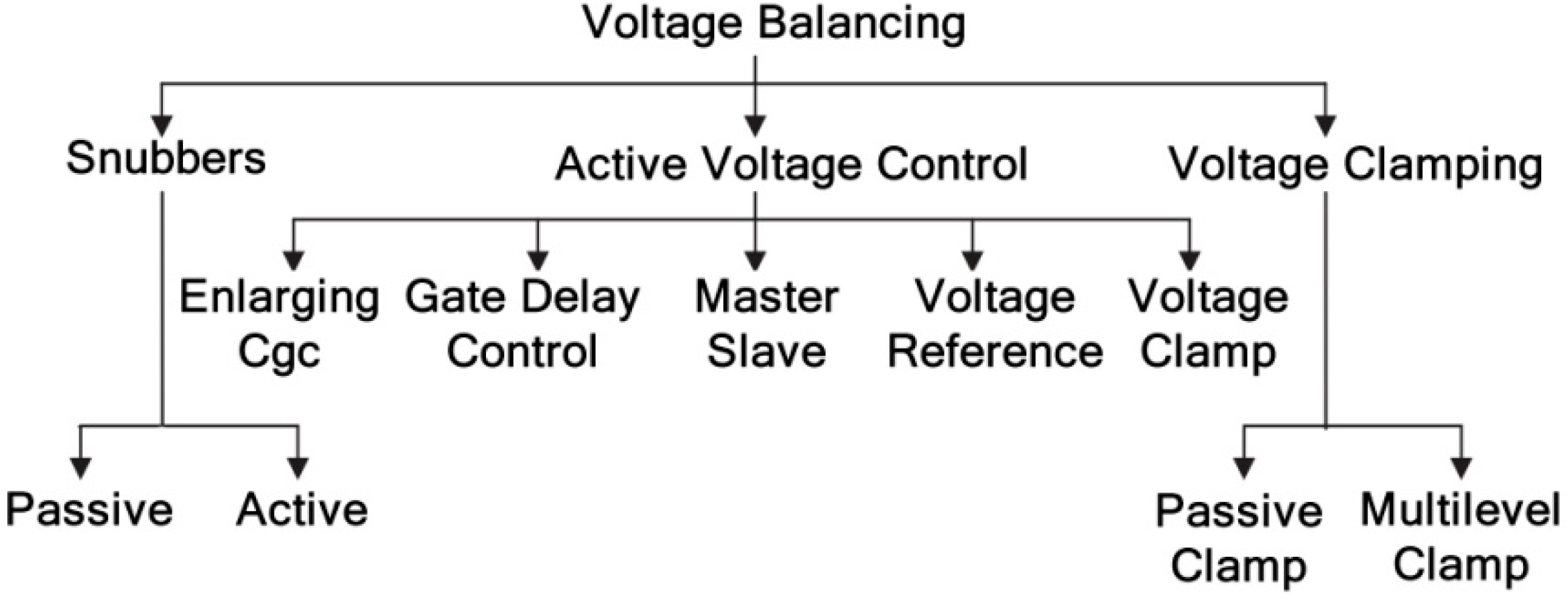
Figure 2.
Typical series connection voltage sharing issues when no-balancing method is applied: (a) Static voltage unbalance occurring before 35 µs (turn-on) and after 65 µs (turn-off) instants; (b) voltage zoom on the turn-on transient showing a poor dynamic voltage sharing [4].
Figure 2.
Typical series connection voltage sharing issues when no-balancing method is applied: (a) Static voltage unbalance occurring before 35 µs (turn-on) and after 65 µs (turn-off) instants; (b) voltage zoom on the turn-on transient showing a poor dynamic voltage sharing [4].
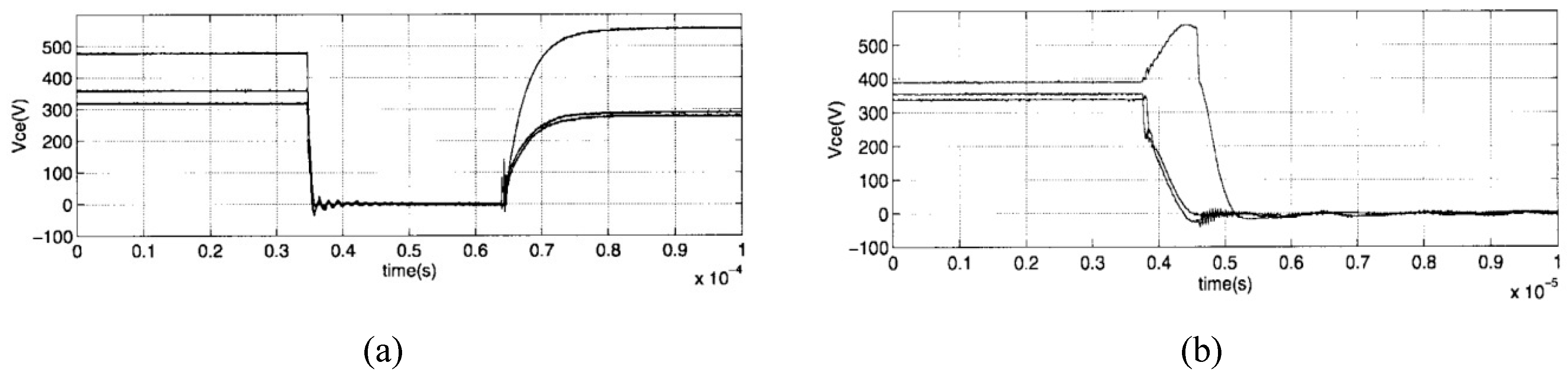
Figure 3.
Control structure with a gate balancing core for parallel firing signals.
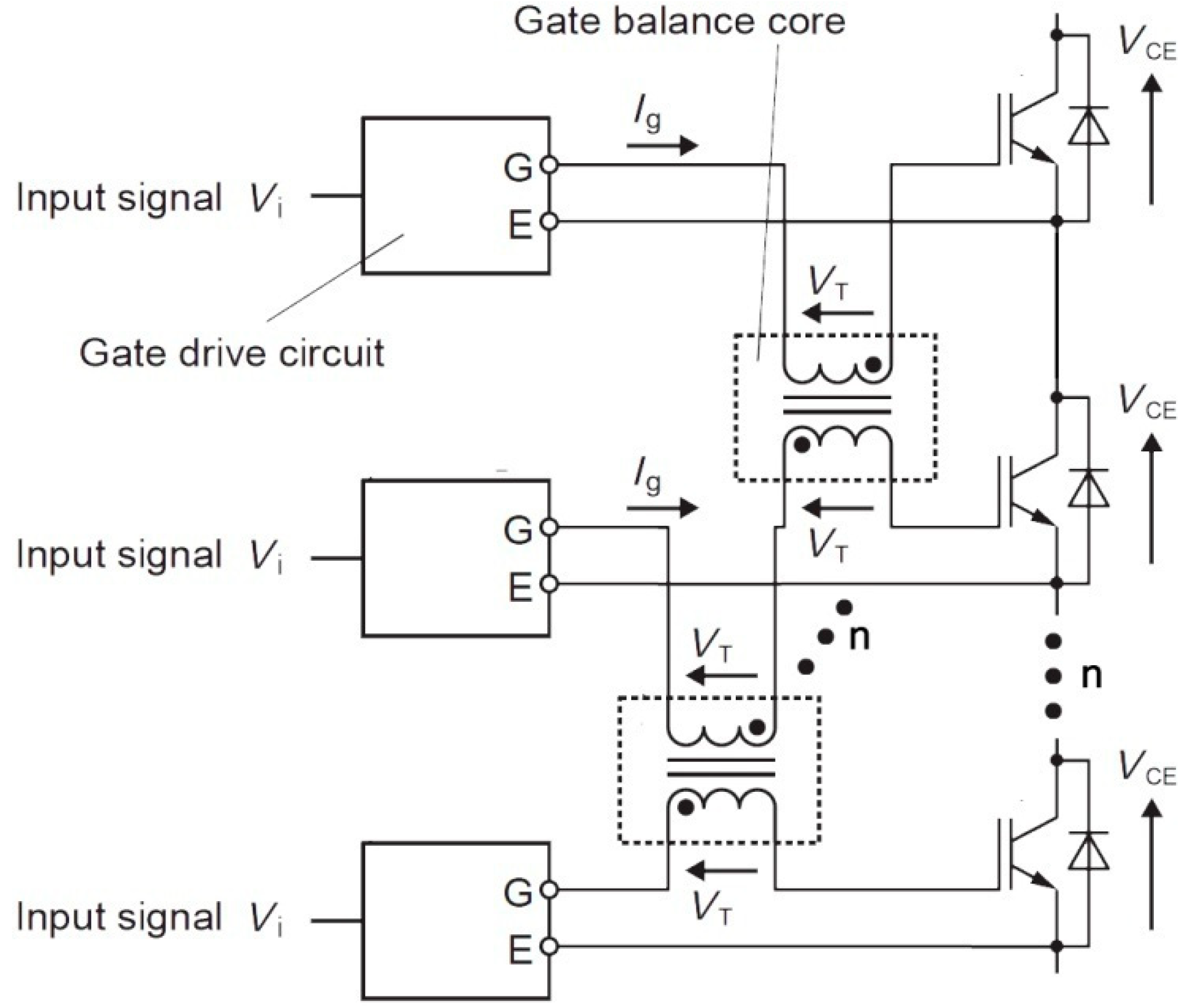
Figure 4.
Double galvanic insulated firing circuit.
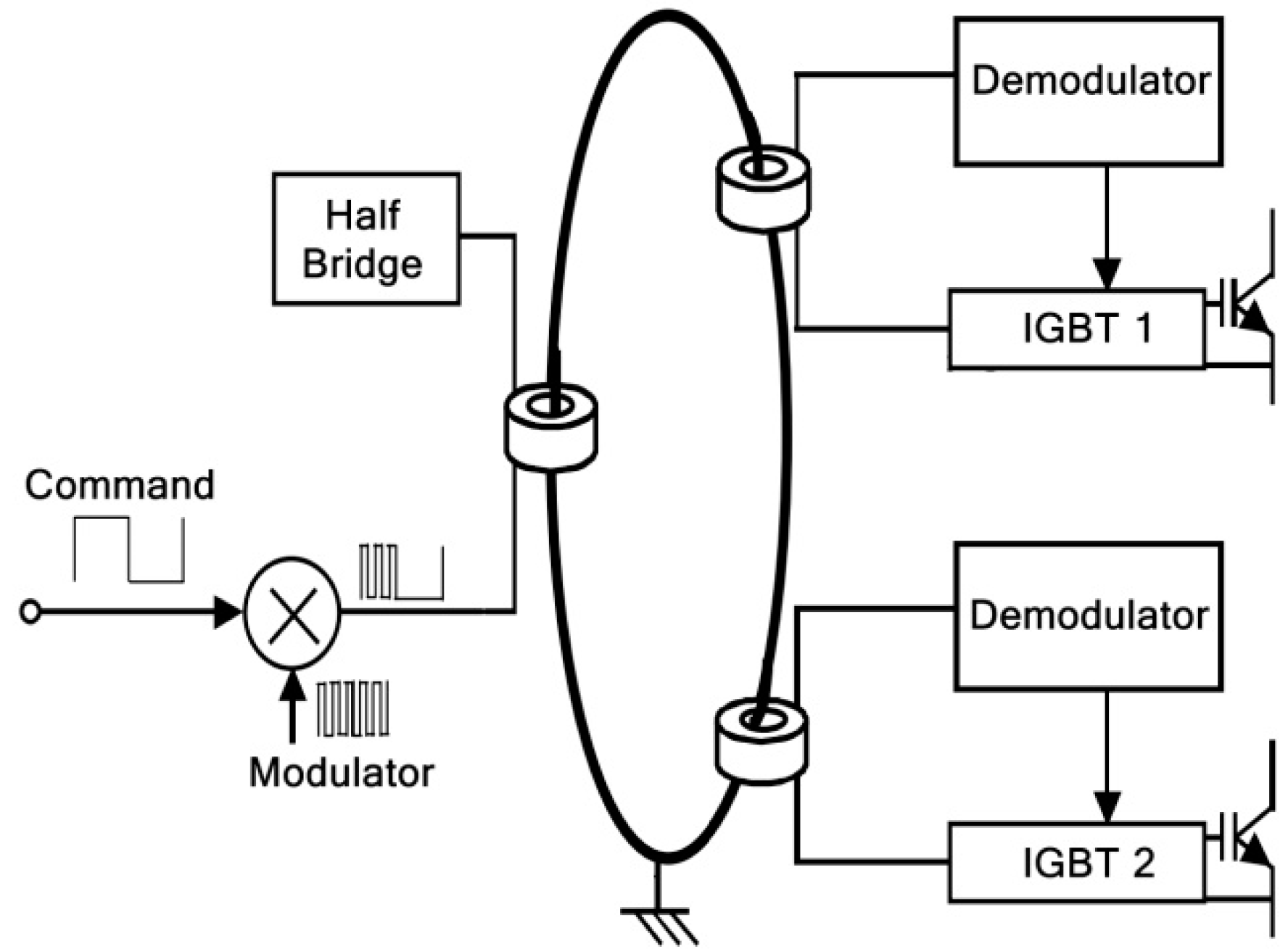
Figure 5.
Schematic of the firing circuit with a synchronous rectifier, two primary simple magnetic loops, based on the thyristor firing concept.
Figure 5.
Schematic of the firing circuit with a synchronous rectifier, two primary simple magnetic loops, based on the thyristor firing concept.
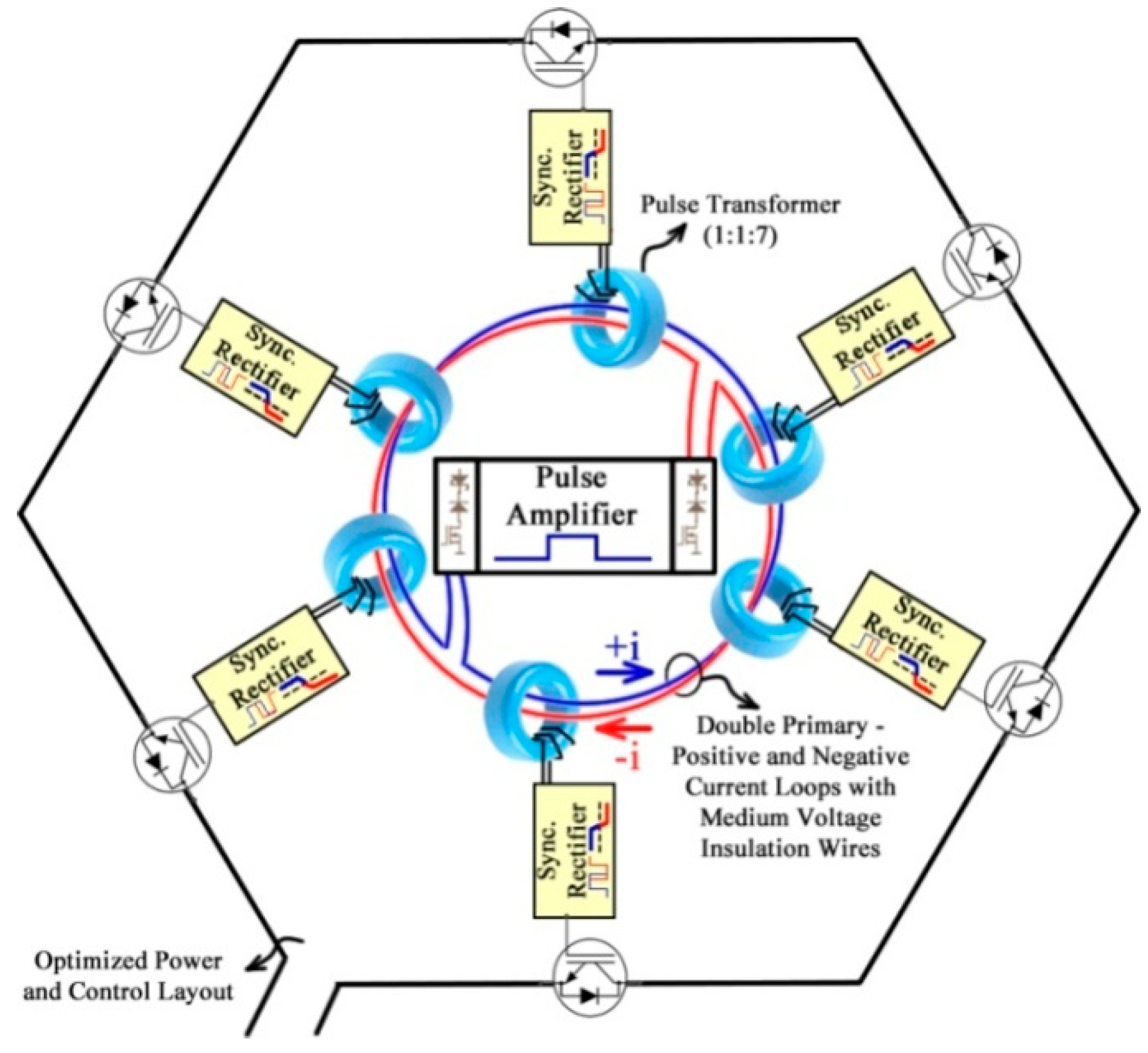
Figure 6.
Gate storage characteristic due to its parasitic capacitance considering a turn-on or turn-off command through a double primary pulse transformer and, also, the clamping circuit setting the on and off levels of the gate voltage.
Figure 6.
Gate storage characteristic due to its parasitic capacitance considering a turn-on or turn-off command through a double primary pulse transformer and, also, the clamping circuit setting the on and off levels of the gate voltage.

Figure 7.
Breakdown of the firing circuit with synchronous rectifier, single and double primary magnetic link, based on the thyristor firing concept.
Figure 7.
Breakdown of the firing circuit with synchronous rectifier, single and double primary magnetic link, based on the thyristor firing concept.
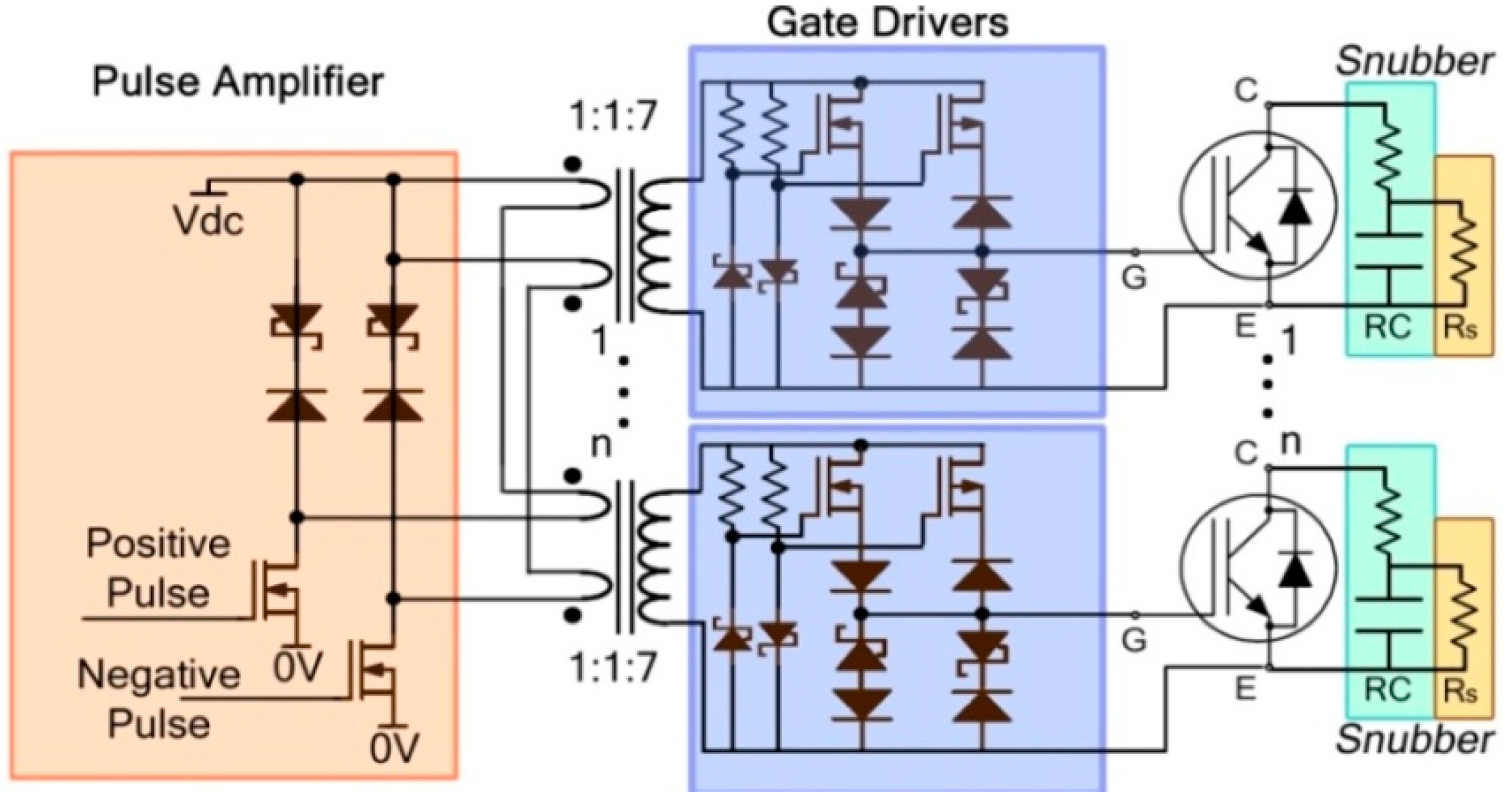
Figure 8.
Upper and lower view of the integrated power sub-module with six serial IGBTs, gate driver circuits and snubbers.
Figure 8.
Upper and lower view of the integrated power sub-module with six serial IGBTs, gate driver circuits and snubbers.

Figure 9.
Variation of the gate-emitter voltage during the switching transient for different blocking voltages (0 V, 100 V and 200 V). The “self-turn-on” and “negative gate capacitance” physical effects were identified, resulting in the natural intrinsic balancing of the collector-emitter voltage.
Figure 9.
Variation of the gate-emitter voltage during the switching transient for different blocking voltages (0 V, 100 V and 200 V). The “self-turn-on” and “negative gate capacitance” physical effects were identified, resulting in the natural intrinsic balancing of the collector-emitter voltage.
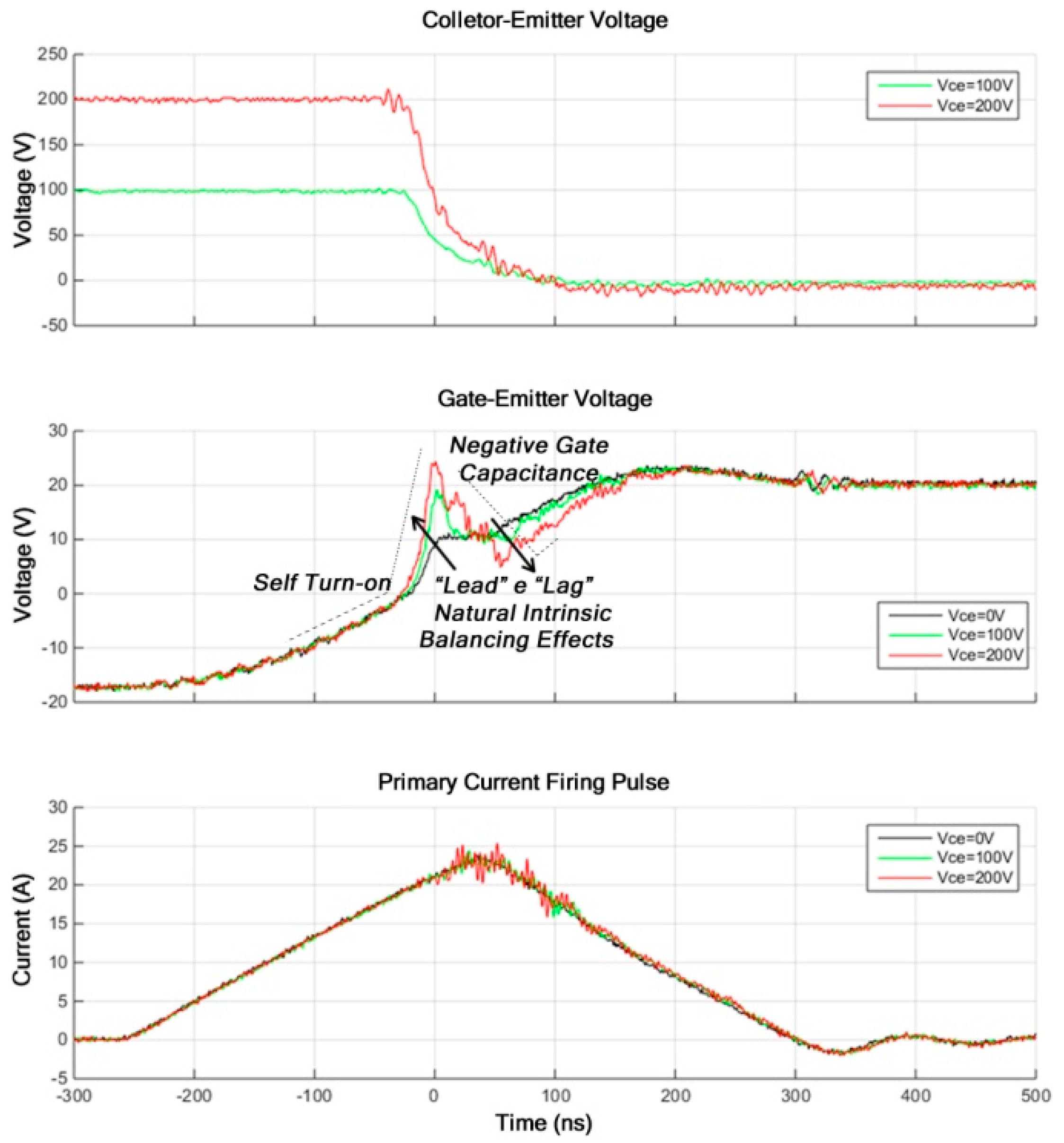
Figure 10.
Power diagram of the test bench.
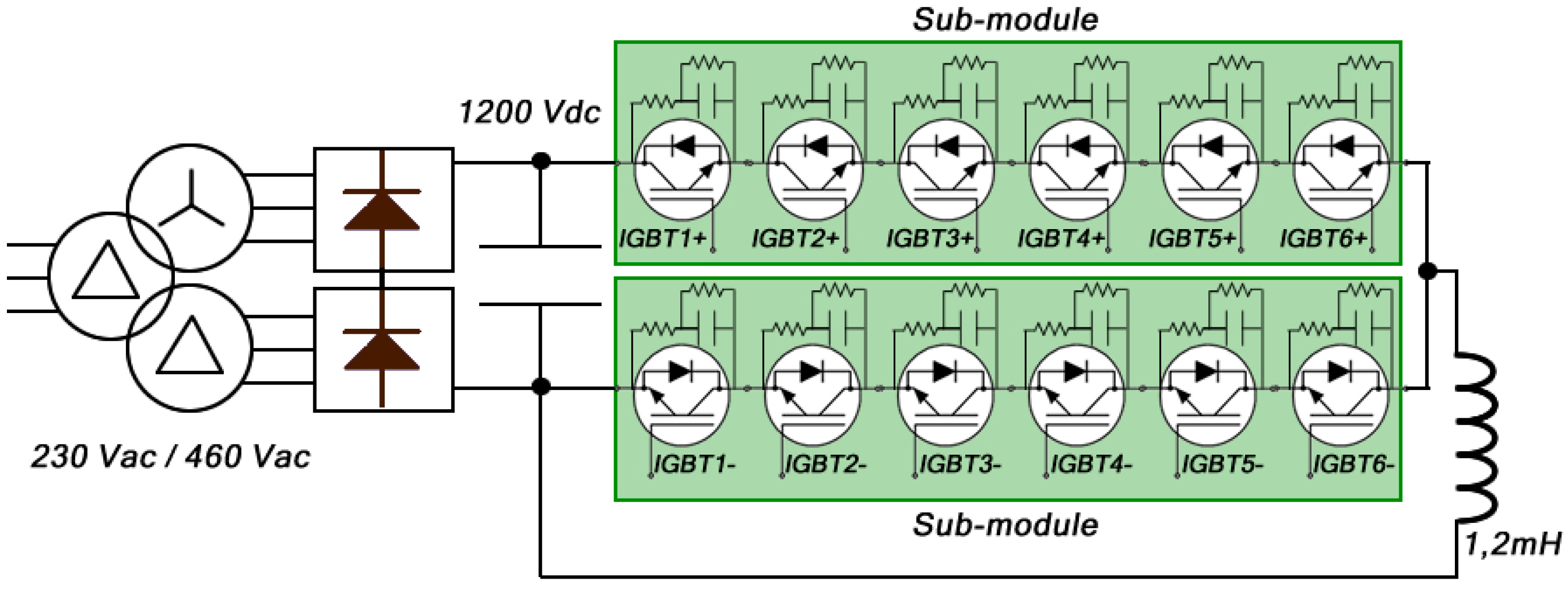
Figure 11.
Photos of the top and bottom view of the hexagonal sub-module.

Figure 12.
Perfect synchronization between the gate-emitter (Vge) voltages of the six series-connected IGBTs. The primary current pulses are shown proving the temporal determinism of each event.
Figure 12.
Perfect synchronization between the gate-emitter (Vge) voltages of the six series-connected IGBTs. The primary current pulses are shown proving the temporal determinism of each event.

Figure 13.
Turn-on switching under snubberless condition. The Vce and Vge voltages of the six series connected IGBTs are shown, as well as the collector current (Ic), showing the effects of the natural intrinsic balancing through gate-emitter voltage.
Figure 13.
Turn-on switching under snubberless condition. The Vce and Vge voltages of the six series connected IGBTs are shown, as well as the collector current (Ic), showing the effects of the natural intrinsic balancing through gate-emitter voltage.

Figure 14.
Turn-off switching under snubberless condition. The Vce and Vge voltages of the six series connected IGBTs are shown, as well as the collector current (Ic), with details for the Miller and negative gate capacitance effects, more apparent during the turn-off transient.
Figure 14.
Turn-off switching under snubberless condition. The Vce and Vge voltages of the six series connected IGBTs are shown, as well as the collector current (Ic), with details for the Miller and negative gate capacitance effects, more apparent during the turn-off transient.

Figure 15.
Turn-on switching with no-load current, showing the current of the snubber’s circuits (negative side devices). The perfect balance of the Vce voltages of the devices was verified.
Figure 15.
Turn-on switching with no-load current, showing the current of the snubber’s circuits (negative side devices). The perfect balance of the Vce voltages of the devices was verified.

Figure 16.
Turn-on switching with 30 A load current, evidencing an increase in the effects of the natural intrinsic balance with the increase of the collector current, imposing an optimal voltage sharing among the devices.
Figure 16.
Turn-on switching with 30 A load current, evidencing an increase in the effects of the natural intrinsic balance with the increase of the collector current, imposing an optimal voltage sharing among the devices.

Figure 17.
Turn-on switching with 60 A load current, reinforcing the previous result on the increase of the effects of the natural intrinsic balancing with the increase of the collector current.
Figure 17.
Turn-on switching with 60 A load current, reinforcing the previous result on the increase of the effects of the natural intrinsic balancing with the increase of the collector current.

Figure 18.
Turn-off switching with 30 A load current showing an excellent voltage sharing among the devices. The Miller and negative gate capacitance effects are clearly seen.
Figure 18.
Turn-off switching with 30 A load current showing an excellent voltage sharing among the devices. The Miller and negative gate capacitance effects are clearly seen.

Figure 19.
Turn-off switching with 60 A load current. The increase in the natural intrinsic balancing effects with the increase of the collector current, from instant 430 ns is also seen.
Figure 19.
Turn-off switching with 60 A load current. The increase in the natural intrinsic balancing effects with the increase of the collector current, from instant 430 ns is also seen.

© 2019 by the authors. Licensee MDPI, Basel, Switzerland. This article is an open access article distributed under the terms and conditions of the Creative Commons Attribution (CC BY) license (http://creativecommons.org/licenses/by/4.0/).
Share and Cite
MDPI and ACS Style
Fortes, G.O.; Mendes, M.A.S.; Cortizo, P.C. Integrated Solution for Driving Series-Connected IGBTs and Its Natural Intrinsic Balancing. Energies 2019, 12, 2406. https://doi.org/10.3390/en12122406
AMA Style
Fortes GO, Mendes MAS, Cortizo PC. Integrated Solution for Driving Series-Connected IGBTs and Its Natural Intrinsic Balancing. Energies. 2019; 12(12):2406. https://doi.org/10.3390/en12122406
Chicago/Turabian StyleFortes, Gustavo O., Marcos A. S. Mendes, and Porfírio C. Cortizo. 2019. "Integrated Solution for Driving Series-Connected IGBTs and Its Natural Intrinsic Balancing" Energies 12, no. 12: 2406. https://doi.org/10.3390/en12122406
Note that from the first issue of 2016, this journal uses article numbers instead of page numbers. See further details here.