A New Coupling Solution for G3-PLC Employment in MV Smart Grids
by
 , , , ,
Giovanni Artale
1, 
Antonio Cataliotti
1,
Valentina Cosentino
1,*,
Dario Di Cara
2,
Riccardo Fiorelli
3,
Salvatore Guaiana
1,
Nicola Panzavecchia
2 and
Giovanni Tinè
2 1
Department of Engineering, Università degli Studi di Palermo, 90128 Palermo, Italy
2
Institute of Marine Engineering (INM), National Research Council (CNR), 90146 Palermo, Italy
3
STMicroelectronics S.r.l., 20864 Agrate, Italy
*
Author to whom correspondence should be addressed.
Energies 2019, 12(13), 2474; https://doi.org/10.3390/en12132474
Submission received: 19 May 2019
/
Revised: 12 June 2019
/
Accepted: 25 June 2019
/
Published: 27 June 2019
(This article belongs to the Special Issue Real-time Communications for Smart Grids and Industry)
Abstract
:This paper proposes a new coupling solution for transmitting narrowband multicarrier power line communication (PLC) signals over medium voltage (MV) power lines. The proposed system is based on an innovative PLC coupling principle, patented by the authors, which exploits the capacitive divider embedded in voltage detecting systems (VDS) already installed inside the MV switchboard. Thus, no dedicated couplers have to be installed and no switchboard modifications or energy interruptions are needed. This allows a significant cost reduction of MV PLC implementation. A first prototype of the proposed coupling system was presented in previous papers: it had a 15 kHz bandwidth useful to couple single carrier PSK modulated PLC signals with a center frequency from 50–200 kHz. In this paper, a new prototype is developed with a larger bandwidth, up to 164 kHz, thus allowing to couple multicarrier G3-PLC signals using orthogonal frequency division multiplexing (OFDM) digital modulation. This modulation ensures a more robust communication even in harsh power line channels. In the paper, the new coupling system design is described in detail. A new procedure is presented for tuning the coupling system parameters at first installation in a generic MV switchboard. Finally, laboratory and in-field experimental test results are reported and discussed. The coupling performances are evaluated measuring the throughput and success rate in the case of both 18 and 36 subcarriers, in one of the different tone masks standardized for the FCC-above CENELEC band (that is, from 154.6875–487.5 kHz). The experimental results show an efficient behavior of the proposed coupler allowing a two-way communication of G3-PLC OFDM signals on MV networks.
1. Introduction
The need of a communication system is a fundamental requirement for modern medium voltage (MV) distribution networks, where, in the near future, a high increase of information exchanges is expected between distribution system operators (DSO), users, and prosumers for the implementation of innovative applications, such as secondary substation automation, monitoring of energy flows, distributed generation, energy storage systems interaction, and so on [1,2,3,4,5,6,7,8].
Wireless or GSM systems are usually recommended for MV/LV secondary substation connection to DSO control centers. On the other hand, these communication systems encounter the intrinsic costs of commercial providers and they can have low reliability (especially in adverse weather conditions). Narrowband power line communication (PLC) over MV networks can be an alternative or a redundant solution. They can also be used in hybrid systems based on different communication technologies to ensure robustness, reliability, and redundancy [9,10,11,12,13,14]. PLC, in fact, has the great advantage of no additional costs for the communication service provider because electric lines are usually owned by the DSO and they are under its direct and secure control. PLC also ensures higher security against cyber-attacks, as potential hackers cannot easily access the communication system [15]. Moreover, the reliability of this technology is already demonstrated by its wide implementation in low-voltage (LV) networks to support various intelligent applications (automatic meter reading, demand-side management, and so on) [16,17,18,19,20,21,22,23]. As regards reliability issues, different modulation techniques were experimented from the first implementations. The first generation of smart meters widely adopted single-carrier digital modulations, in particular frequency-shift keying (FSK) and phase-shift keying (PSK). New international standards have suggested more robust and reliable modulation techniques and protocols based on orthogonal frequency division multiplexing (OFDM) modulation. These techniques will be also adopted for the new generations of smart meters and the implementation of other smart applications in LV networks [24,25,26,27].
As regards the implementation of PLC in MV distribution power systems, recent research activities have been carried out to investigate and model MV lines and MV/LV power transformers’ behavior in the frequency range of interest [28,29,30,31,32,33]. However, the central issue for the diffusion of PLC in MV power systems is related to the required costs for signal couplers installation. In fact, MV couplers should be installed both in primary substation (at MV bus-bars) and in all MV/LV secondary substations. The very large number of couplers to be installed involves not only the costs of the equipment, but also those of the MV switchboard modifications and the energy interruptions for their installation.
To face these issues the authors have developed a new coupling principle [34], which allows transmitting and receiving PLC signals by using the voltage detection system (VDS) capacitive dividers, already installed in the MV switchgear of the distribution network’s substations. In previous works, a first coupler prototype was presented, where the PLC modem and the VDS socket on the MV switchboard front panel were connected by means of an appropriate interface card. The interface card was constituted by a transmission and a reception circuit. Variable inductors are used in both circuits to obtain a resonance condition with the equivalent capacitance Ceq seen from the VDS socket terminals. Thus, the proposed coupler is based on a different coupling principle with respect to commercial capacitive couplers, where an inductance is usually connected in series between MV capacitance and earth. In the proposed solution, in fact, the variable inductors are connected in parallel to the capacitance Ceq to earth. In addition to the parallel variable inductors, the first prototype also included an amplification stage followed by an impedance matching circuit in the transmission path and a pass-band filter in the reception path. The developed prototype featured a 15 kHz 6 dB bandwidth, which is sufficient to couple single carrier narrowband (NB) PLC signals with FSK or n-PSK modulation technique and baud rate of 9600 baud/s. Laboratory and in-field tests performed with this first prototype at different center frequencies up to 200 kHz were presented in previous works [35,36,37].
This paper investigates the possibility to use the same coupling principle to couple multicarrier G3-PLC signals with OFDM digital modulation in the FCC band. In this case, a bandwidth larger than the 15 kHz of the first prototype is required to couple a signal composed by at least 18 sub-carriers (with center frequencies equally spaced by 4.6875 kHz). To this aim, a new prototype of MV PLC coupler is developed, which features a bandwidth extendable up to 164 kHz. With respect to the first prototype, the new solution proposed in this paper has some modifications both in transmission and reception paths.
As regards the transmission path:
- a second amplification stage, consisting in a push-pull power amplifier, was added to realize a current-buffering circuit, which supplies the high current required by the LC load circuit in resonance conditions;
- a new tuning procedure was developed to select the variable inductors values at first installation of the new MV coupler in a generic MV switchboard;
- a microcontroller was added and a related graphical user interface (GUI) was implemented to perform the above-mentioned tuning procedure;
- two finely-variable inductors were implemented by connecting in series several inductors of fixed values, those could be short-circuited by switches controlled by the microcontroller digital outputs. A finer inductance value regulation allows to perform a finer tuning of the resonance condition.
As regards the reception circuit:
- three second-order multiple feedback pass-band active filters were designed; their inputs were connected in parallel, while an adder circuit is used to compose and to amplify their outputs.
- digital resistors were introduced, whose values can be adjusted by the microcontroller to regulate the filter parameters (i.e., center frequencies, bandwidth, gain);
- a new tuning procedure was developed also for the reception circuit, it was implemented in the microcontroller GUI, to select the reception variable inductor and the filter parameters.
The developed new solution allows changing the coupler frequency band to cover each of the standard FCC band tone masks (that is, from 154.6875–487.5 kHz). Since the developed interface board is totally analog, the proposed coupling solution can be used with a generic transceiver. Many tests were performed both in the laboratory and in the field, in the MV network of Favignana, to characterize the coupling system performances in terms of frequency response. Moreover, the communication performances were also verified using an STCOMET transceiver and measuring the throughput and success rate in the FCC band.
The paper is structured as follows: Firstly, technical and regulatory reasons are summarized that led to the adoption of multicarrier OFDM modulation for the PLC field. Secondly, a description is given of new coupling prototype development and its parameter-setting procedure. Finally, laboratory and in-field experimental tests are presented, to verify the proposed solution’s performance.
2. Digital Modulations for PLC in Smart Grid Applications
Narrowband power line communications based on FSK or N-PSK digital modulations have been used for many decades, mainly for smart metering and automation purposes [1,38]. The development of a variety of new services and applications included in smart grid frameworks requires greater reliability. Moreover, background noise, impulsive noise, and narrowband interferences, often observed both in LV and MV distribution networks, can strongly affect the PLC channel, whose parameters and characteristics are very variable depending on site, type of equipment connected, frequency, and time [39]. To overcome these limitations and to provide more robustness to PLC, the international standards have introduced the OFDM modulation techniques. The International Telecommunications Union (ITU) and the Institute of Electrical and Electronics Engineers (IEEE) have set some recommendations for NB-PLC up to 500 kHz based on multi-carrier OFDM: on one hand ITU specifies several narrow-band OFDM techniques (see ITU-T G.9901 [40]) including G3 PLC protocol (ITU-T G.9903 [39]); on the other hand IEEE P1901.2 (IEEE 1901.2- 2013) suggested the application of a similar OFDM technique at the physical layer. An example of a full PLC protocol stack for a smart grid based on the OFDM PHY layer is shown in Figure 1 [41].
The G3-PLC OFDM modulation ensures robust communication even in extremely harsh power line channels. This is obtained by dividing the allowed bandwidth into sub-channels; they can be seen as several independent PSK-modulated signals with different orthogonal noninterfering carrier frequencies. Furthermore, even if background and impulsive noise can determine the loss of some bits, the receiver is able to recover them, thanks to redundancy bits provided by convolutional and Reed-Solomon (RS). The received noise correlation at decoder input is reduced by a time-frequency interleaving scheme. This technique offers data rates that can reach hundreds of kbit/s. In accordance with different standards (CENELEC-A, CENELEC-B, ARIB, and FCC), numerous frequency band-plans are available. According to the used sub-carriers (usually from 16–72) the maximum data rate can vary from 20–185 kbit/s at the physical layer [42].
Different commercial solutions are already available to generate PLC OFDM signals for both direct and alternating current (DC and AC) power lines, in frequency range below 500 kHz. In this work a STMicroelectronics (Geneva, Switzerland) platform is employed, which is the EVLKSTCOMET10-1 evaluation board, based on STCOMET device. It is suitably developed for smart meters applications, as it integrates metrology functions with a modem, which has been developed to enable applications compliant with different standards (EN50065, FCC, ARIB). The STCOMET already embeds a coupling circuit for LV. STCOMET can also support different NB-PLC protocol specifications (PRIME, IEEE 1901.2, G1, G3, METERS AND MORE and others) [43].
For example, according to the ITU-T G.9901 technical specifications, STCOMET can be set to select one frequency band plan (CENELEC A, CENELEC B or FCC). In addition, for each band plan different sub-channels or tone masks can be selected. The FCC band plan (154.6875–487.5 kHz) can be divided into one, two, or four tone masks as shown in Table 1. In the first case, the tone mask is composed of 72 subcarriers, whose center frequencies are equally spaced (4.6875 kHz) in the whole band of about 330 kHz; in the second case (two tone masks) 36 subcarriers are used for each sub band of about 164 kHz; in the last case, 18 sub carriers are used in each tone mask covering a bandwidth of about 80 kHz.
The STCOMET can be programmed via a GUI selecting the sub-carriers which compose the G3-PLC OFDM signal. In this way, the PLC channel can be experimentally characterized (for example by evaluating the SNR) and this can help in selecting the tone mask with the best quality of received signal and avoiding other noisier frequency bands.
3. Coupling System for G3-PLC in MV Networks
One of the fundamental elements of a PLC channel is the coupling device: it is used to inject and receive communication signals into the power network. Different types of coupling devices can be adopted, mainly in dependence of the voltage level and desired performances [16]. A survey on PLC coupling systems is reported in [44]. In the case of MV systems, basically, two type of couplers are used: capacitive and inductive couplers.
Capacitive couplers are directly connected to MV lines. An inductance and/or an isolation transformer are usually connected in series to the MV capacitance [44,45,46,47]. This guarantees high impedance to mains frequency. Moreover, this type of coupler has low insertion losses.
Inductive PLC couplers for MV systems are usually based on an openable magnetic core. Thus, they can be easily positioned around the MV cable also ensuring galvanic isolation [1,44]. Since no direct electric connection is requested, the installation is very easy and does not require service interruptions. The shape and magnetic characteristics of the core, the gap width, and the power cable characteristic impedance have an influence on the coupling efficiency [48,49,50]. A disadvantage of inductive couplers is the intrinsic non-linear behavior of the magnetic core, which can cause distortions and possible saturation of the magnetic core in the case of high currents in power cables.
In any case, the installation of a MV PLC dedicated coupler requires direct and indirect costs for the related equipment, installation, switchboard modification, and eventual service interruptions. To avoid these costs, authors proposed in [34] a new coupling principle which makes use of electrical elements already embedded in the MV switchgears as PLC couplers. In particular, the attention was focused on using VDS capacitive dividers; in fact, according to IEC 61243-5 [51], VDS are usually installed in MV switchboards of major electrical manufacturers, to ensure safety by detecting the presence of mains voltage. VDS capacitive divider output is made available at the switchboard front panel by means of a standardized socket. The voltage detection principle is based on the voltage division on the series of two capacitances, i.e., that of the capacitive isolator and the equivalent capacitance to earth seen from the socket terminals (Ceq). Therefore, connecting a voltmeter to the VDS socket terminals, a low voltage value can be measured proportional to the medium voltage value. Alternatively, the voltage presence can be revealed by means of a removable plug connected at socket terminals, equipped with a light-emitting diode (LED). The authors’ idea is to use the aforesaid VDS socket terminals for injecting and receiving the PLC signal, without modifying any components already installed inside the switchboard.
A first coupling prototype was developed featuring a 6-dB bandwidth of 15 kHz. It was tested with FSK- and n-PSK-modulated PLC signals. In the following sub-sections, the coupling solution principle will be resumed. Then, a new prototype will be presented describing in detail the modification adopted to extend its bandwidth, in order to couple G3-PLC signals with a bandwidth up to 80 or 164 kHz required for 18 or 36 subcarriers, respectively. Moreover, a procedure will be defined to set the coupling system parameters at first installation in a generic MV switchboard.
3.1. The New MV Coupler Prototipe
In general terms, besides high electrical insulation a MV PLC coupler must ensure signal circuit insulation from supply voltage; thus, coupler impedance at mains frequency must be high. On the other hand, the coupler impedance in the PLC frequency band must be low in order to allow transmitting PLC signals with the desired modulation’s technique. It is clear that the simple VDS capacitance series is not suitable to act as PLC coupler. Differently from usual commercial couplers, no further components can be connected in the capacitance series because they are connected to earth inside the switchboard. To deal with this problem, a different coupling approach and a dedicated interface card were designed as explained in the following.
A schematic of the first prototype of interface card is shown in Figure 2 [35]. The interface card has to be connected between the VDS socket terminals and the PLC transceiver. The signal is injected between the cable core and its earth-connected shield (core-to-shield transmission). Two different circuits were designed, one for the reception path and one for the transmission path. Two switches are used to select the desired circuit. They are controlled by a digital terminal of the transceiver. Variable inductors are used in both circuits to obtain a resonance condition with the equivalent capacitance Ceq seen from the VDS socket terminals.
The resonance condition allows obtaining a high impedance path to earth. This guarantees, in transmission, that most part of the transmitted signal is coupled to the medium voltage line rather than being short-circuited to earth. An amplification stage followed by an impedance matching circuit is also used in transmission to increase the amplitude of the injected signal. On the other hand in reception, the signal amplitude voltage is divided between the capacitive isolator and the impedance to earth seen from the VDS terminals (Ceq). The resonant circuit obtained with the variable inductor allows increasing the impedance value to earth, reducing the signal dispersion towards earth and consequently increasing the received signal amplitude measured in parallel. A pass-band active filter is also used in reception to attenuate noise and increase the signal-noise ratio (SNR).
This first prototype featured a 6 dB bandwidth of 15 kHz, which allowed transmitting and receiving FSK and n-PSK modulated signals with carrier frequency from 50–200 kHz, as demonstrated with on field tests presented in [35,36,37].
In this paper a new prototype has been developed to enlarge the coupling bandwidth up to 80 or 164 kHz in order to transmit OFDM signal with 18 or 36 carriers, respectively. The new prototype has some modifications both in transmission and reception circuits. More in detail, two amplification stages are used in transmission, in order to maximize the amplitude of the signal injected in the MV line: the first performs a linear amplification using a low-cost operational amplifier; the second is based on a power amplifier scheme. The transceiver injects the modulated signal into the first amplifier stage that is used as a driver for the power amplifier to realize a current-buffering circuit. The power stage consists in a push-pull amplifier, which is used to supply the high current required by the LC load circuit in resonance conditions. The resonant behavior is obtained by means of two variable inductors, which are adjusted to create an impedance matching with the equivalent capacitance Ceq. The variable inductors are constituted by a series of inductors of fixed value (from 3 µH to 1.5 mH); each of them can be short-circuited by means of controlled switches. The developed GUI selects the inductance value from those available by using the microcontroller digital pin connected to the controlled switches. A schematic of the new prototype of interface card is shown in Figure 3.
Inductors are adjusted to obtain a series circuit with a resonance at tone mask center frequency , a sufficiently wide bandwidth B, and a low Q factor (calculated as ). This allows maximizing the signal amplitude in the MV line for all the considered OFDM signal carriers.
The received signal is measured in parallel of a resonant system which features high impedance in the resonance frequency range with resonant circuit losses. Thus, to reduce the influence of the Req resonance resistance, whose value is not constant and varies with the frequency range used, it is necessary to mismatch the impedance towards the filter stage. This explains the use of the buffer that decouples the impedances.
Moreover, with respect to the first prototype, the reception stage was modified introducing an amplification system consisting in three second-order multiple feedback pass-band active filters (PBAF) with different central frequencies, whose scheme is reported in Figure 4.
The use of three PBAF together with the tuning procedure, described in Section 3.2, is proposed to obtain a good equalization of the received signal in the whole frequency range of interest. In fact, worst communication results were experimentally obtained when the signal was not equalized, as shown in Section 4. Further advantages of the flat frequency response are listed in Section 3.2. It should be also underlined that the spectral flatness is also a requirements for the transmitter specifications, as reported in the standard ITU-T G.9903 [39], which requires a transmitter flatness between the subcarriers not more than 5 dB (when measured using a peak detector with a 200 Hz bandwidth and loaded on an artificial mains network).
Each filter amplifies only a portion of the band in order to guarantee an equalization of the received signal. The output of the LC resonant group is connected at the same time to the inputs of the three filters; their outputs are connected to an adder circuit which amplifies the composed signal. A proper choice of the active filter’s parameters allow obtaining the desired flat bandwidth.
Analyzing in detail the circuit of Figure 4, choosing C1 = C2 = C, the transfer function of the active filter can be written as:
The parameters were indexed with a i (variable from 1 to 3) to indicate that they are different for each of the three filters.
The center frequency , the gain and the bandwidth of the filter can be then expressed as:
Therefore, acting on the resistor values it is possible to adjust the filter gain, the bandwidth, and its central frequency in order to equalize the received signal amplitude whatever is the chosen tone mask.
The filters outputs are connected to the adder circuit shown in Figure 5. Since the input impedances are equal for the three filters, the output voltage can be obtained as:
Then the transfer function of the whole circuit is:
where , , and are the transfer functions of the three filters.
3.2. Coupling System Tuning Procedure
As previously underlined, each VDS installed in a MV switchboard presents an equivalent capacitance Ceq, whose value is a priori unknown, because it depends both on the internal components of the VDS and the MV switchboard and on stray capacitances. Thus, at first installation of the MV coupling system, the interface card parameters should be adjusted to match the unknown Ceq. Since mains voltage has no influence on the tuning procedure at PLC signal frequencies, no energy interruption is needed even at first installation of the coupling solution. The tuning procedure is implemented using an ARM microcontroller on board of the new prototype. More in detail, the microcontroller can vary the inductors by means of some digital outputs, which act on the short-circuiting switches of the inductors series. The variable resistances of the filters are implemented using digital rheostats with SPI interfaces, which are connected to the correspondent serial port of the microcontroller. In this way, the microcontroller can adjust the inductors and the filters parameters to obtain the resonances, building up the overall flat response for each selected tone mask.
Even if OFDM systems could be normally robust enough (more than single carrier-based communications) against frequency selective fadings, it was found experimentally that the worst communication results were obtained when the signal was not equalized, as shown later in the experimental results.
Thus, a tuning procedure is defined in the following to obtain a flat frequency response, which have the following advantages:
- it helps reducing the losses due to coupling system selectivity;
- it helps having a better transmission efficiency for all the subcarriers;
- it guarantees better reception performances, as also suggested by the transceiver manufacture specifications.
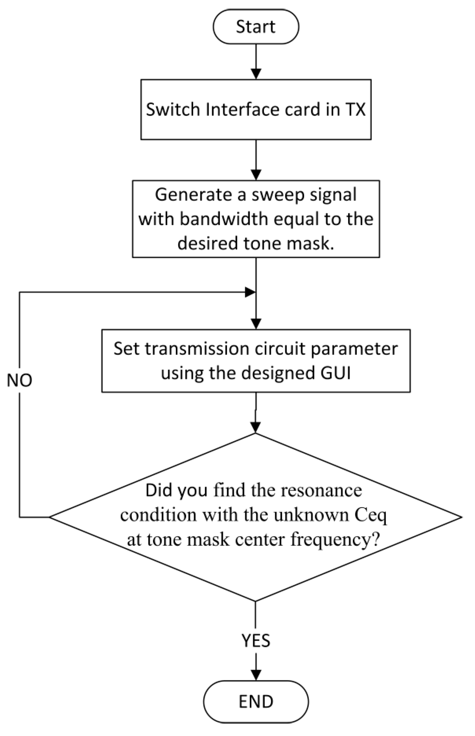
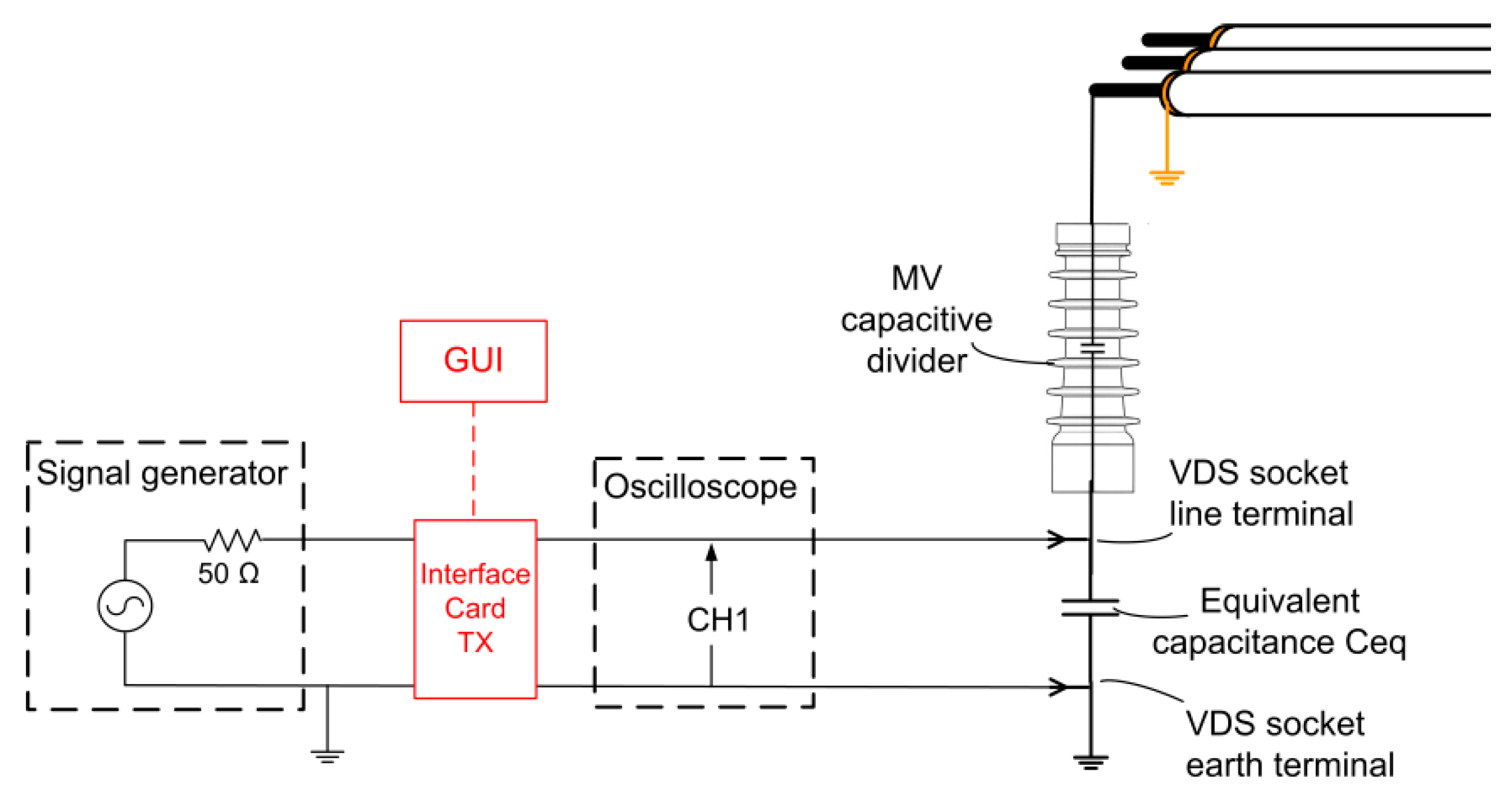
The tuning procedure is divided in two steps. Firstly, the transmission (Tx) circuit parameters are set. A flow chart of the transmission circuit tuning procedure is shown in Figure 6. The interface card input and output are connected to a waveform generator and the VDS socket terminals, respectively, as shown in Figure 7. The generated sweep signal is a sinusoidal signal whose frequency is linearly varied in the whole frequency range of the selected tone mask. An oscilloscope is connected at interface card output, i.e., in parallel with VDS socket terminals. Thanks to its high input impedance, it has no influence on the parameter tuning. The oscilloscope calculated the signal frequency spectrum by means of the Fast Fourier Transform (FFT). A GUI was designed for the microcontroller to set the inductance values in order to find the resonance condition with the unknown Ceq at the tone mask center frequency.
Once transmission circuit parameters are set for both secondary substations under test, then the reception circuit parameters can be adjusted. A sweep signal is sent from one substation by using the already-set transmission circuit parameter. In the second substation, the reception circuit parameters are adjusted to obtain a 6 dB bandwidth of 80 kHz in the case of 18 subcarriers and 164 kHz in the case of 32 subcarriers. More in detail, firstly the active filters resistors are set by using Equations (2)–(4) to have proper gains, Q factors and central frequencies which allow covering the desired tone mask. Then the reception inductors are set to obtain a resonant behavior with Ceq, which results in a high impedance to earth. This allows a higher PLC signal voltage across the VDS socket terminal with respect to the capacitive divider alone, thus obtaining higher amplitude of the received signal. Finally, the active filters gains, Q factors and central frequencies are finely set to equalize the received signal and to obtain the desired flat response in the whole tone mask. A flow chart of the reception circuit tuning procedure is shown in Figure 8. A scheme of the test system for the tuning of the interface card reception circuit (Rx) is shown in Figure 9. Additionally, in this case, the microcontroller GUI is used to set the variable parameters of the interface card reception circuit (Rx) and an oscilloscope is connected at the interface card output to measure the received signal spectrum, which is closed on the input impedance of the transceiver STCOMET.
4. Laboratory Tests
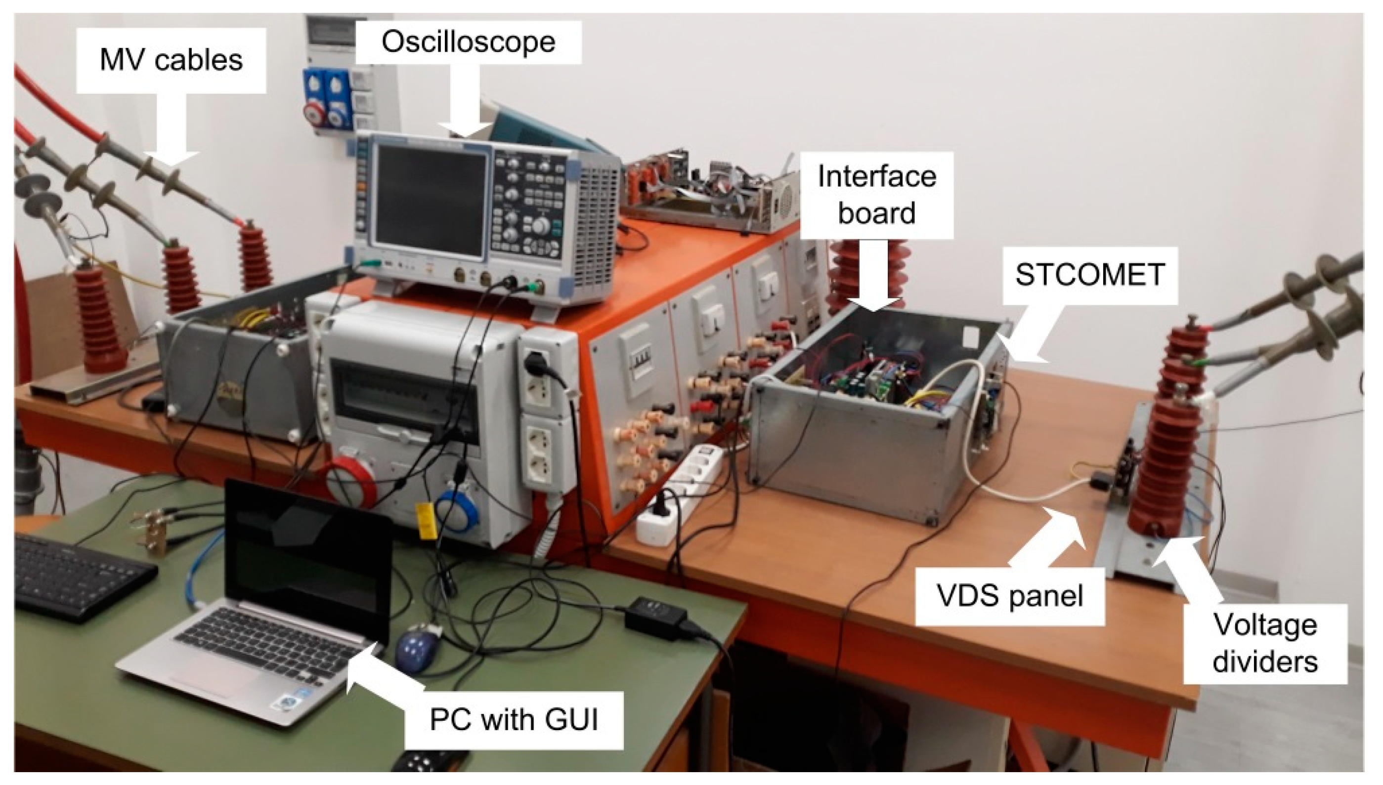
Laboratory tests were performed to verify the new prototype bandwidth and its capability of transmitting OFDM-modulated signals effectively. These tests were carried out in the absence of mains voltage. The test bench is shown in Figure 10. Two sets of three capacitive dividers are connected by three unipolar MV cables (MV-shielded cables type RG7H1R with aluminum core and 50 mm2 cross-section). A VDS panel is connected to each capacitive dividers set. A standard was adapted to connect an interface card prototype at each VDS panel. To verify the novel coupling system performance levels, two tests are performed: a frequency response test and a transmission test.
As described in the previous section, the frequency response analysis is aimed at tuning the interface card parameters, both in transmission and reception; this allows obtaining a flat frequency response across the tone mask under test. The sweep signal is applied to the transmitting interface card by means of the signal generator (Tektronix AFG1022 (Beaverton, OR, USA)). The generated signal has an amplitude of 1.5 VPP (peak to peak) and a SPAN equal to the tone mask frequency. A digital oscilloscope (Rohde and Schwarz RTO 1044 (Munich, Germany)) allows measuring the signals’ spectra (both transmitted and received) at interface card transceiver terminals; and FFT analysis is performed with a resolution bandwidth (RBW) of 300 Hz.
For example, the results of the frequency response obtained for the tone mask 323.4375–403.125 kHz are shown in Figure 11. The figure shows a comparison between the frequency responses obtained with and without tuning the inductors and the filter parameters in reception. It can be seen how the tuning procedure allows obtaining a signal higher in amplitude and with an enough flat frequency response in the whole tone mask, i.e., with a maximum difference of 6 dB in the considered 80 kHz.
The results of a test in the case of a larger bandwidth of 164 kHz is shown in Figure 12. It corresponds to the tone mask 154.6875–318.75 kHz. Additionally, in this case, a flat bandwidth was obtained even if with reduced amplitude respect to that of Figure 11.
Once the parameters are tuned for each tone mask, communication tests can be performed. Different tests were performed to verify the proposed MV coupler transmission capability for different tone masks with both 18 and 36 subcarriers. Two STCOMET transceivers were employed to transmit and receive the PLC signal and 1000 packets were sent for each test. STCOMET transceiver was used to transmit and to receive OFDM signals, changing its sub-carriers modulation techniques (among the following ROBO, BPSK, QPSK, 8PSK); moreover, two different modes can be selected for each modulation, i.e., coherent and differential. The coupling performances were tested measuring throughput and SNR. In the case when 18 sub carriers are used a 100% success rate was obtained for all modulations and for all tone masks in the FCC band. The maximum value of throughput (36 kbit/s) was obtained with 8PSK differential modulation (see Table 2). The measured SNR was always greater than 20 dB. The signal spectrum measured for the 323.4375–403.125 kHz tone mask is shown in Figure 13. Additinally, in this case, the figure shows a comparison between the frequency spectra obtained with and without tuning the inductors and the filter parameters in reception. This allows showing the positive effect of the tuning procedure both in terms of signal amplitude and flatness of the frequency response in the whole tone mask. This is also confirmed by the results shown in Table 3, obtained in the communication tests without tuning the inductors and the filter parameters in reception. As can be seen, even with the Robo modulation, low success rate, and SNR were obtained.
Additionally, in the case of 36 subcarriers, a 100% of success rate was obtained in the laboratory. The best results in terms of throughput are reported in Table 4. A throughput of 50 kbit/s was obtained with 8PSK differential modulation, higher than that measured in the case of 18 subcarriers. On the other hand, a lower SNR was measured. This is due to the coupling system behavior: an increase in the bandwidth, in fact, corresponds to a signal amplitude reduction, while the measured noise amplitude remains almost the same. The signal amplitude reduction can be also verified comparing the signal spectrum measured with 36 subcarriers (tone mask: 154.6875–318.750 kHz) shown in Figure 14 with that of Figure 13.
5. Field Tests
Communication in-field tests were carried out in the real distribution network of Favignana (a small island of Mediterranean Sea). The portion of MV network used as test site is shown with the purple color line in Figure 15; secondary substations “Sub. 6 - Gen. Di Vita” and “Sub. 9 - 4 Vanelle” were chosen for the tests. Sub. 9 is a nodal substation, with one incoming and three departing lines; it has five MV switchgears, i.e., one for each line and the last one for the MV/LV power transformer (20/0.4 kV/kV, 250 kVA). One departing line connects Sub. 9 with Sub. 6. This last one is a bypass substation; it has three MV switchgears: two for the arriving and departing MV lines and one for the MV/LV power transformer (20/0.4 kV/kV, 160 kVA). The connection between Sub. 9 and Sub.6 is a cable line 1.1 km long; the cables are of RG7H1R type (unipolar, copper shield, aluminum core, 50 mm2 section). Bi-directional transmission tests were performed, i.e., transmitting from substation Sub. 6 and receiving in substation Sub. 9, and vice versa. All in-field tests were carried out in the presence of mains medium voltage, without any energy interruption.
The test bench in Sub. 9 is shown in Figure 16; the depicted experimental setup includes the STCOMET device, the interface card prototype, and its connection with the VDS socket panel of the MV line linked to Sub. 6.
The tests were aimed at evaluating the coupling performances in all the tone masks of the FCC frequency range (154.6875–487.5 kHz), both in the case of 18 and 36 subcarriers. The tests consisted in the following three steps for each tone mask:
- interface card tuning;
- noise measurement;
- transmission tests.
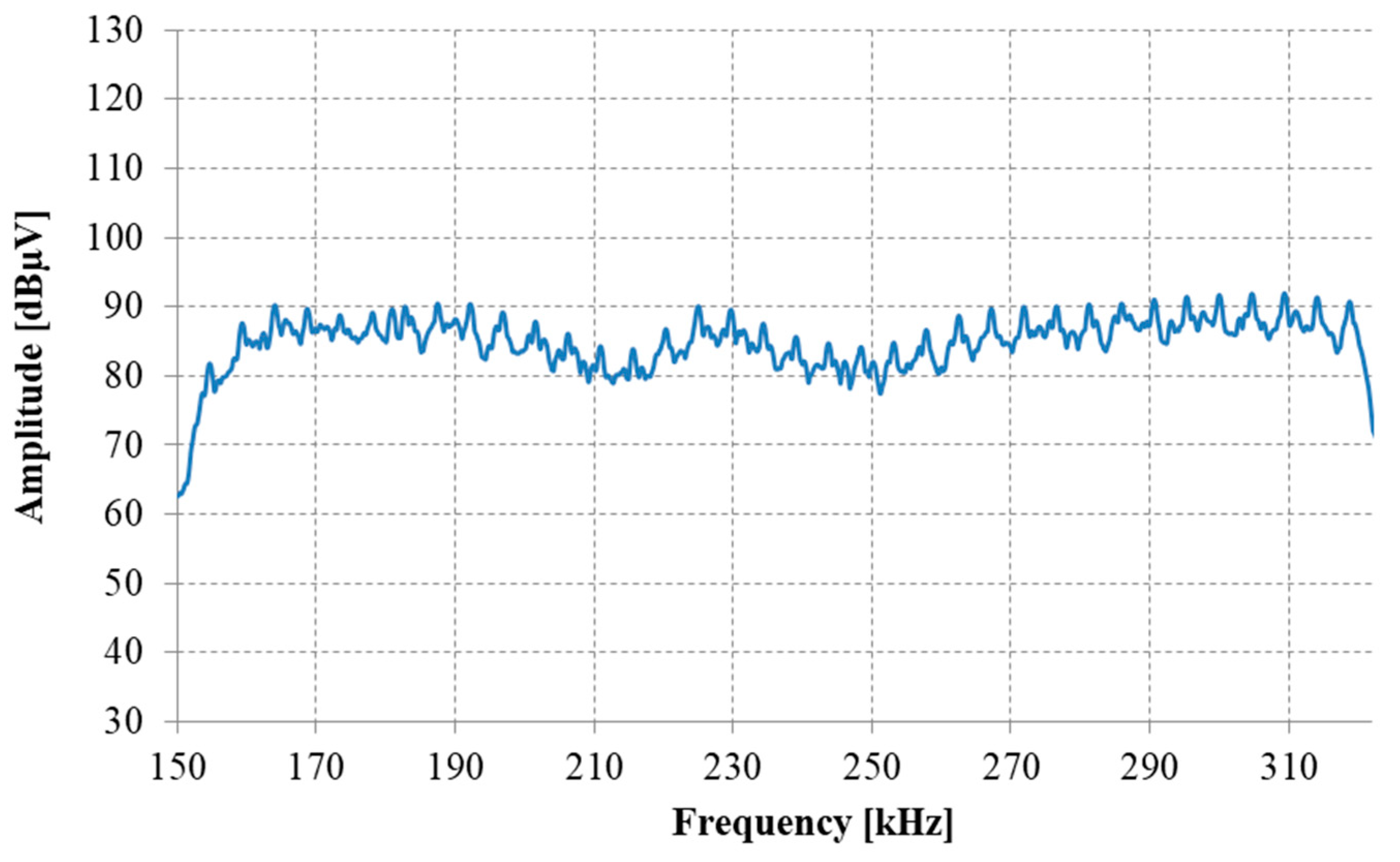
Firstly, the tuning procedure is performed as described in Section 3.2: in each substation the interface card parameters are varied to obtain the resonant response with the unknown capacitance of the VDS panel embedded in the considered switchgear and a flat frequency response at the reception circuit output. This procedure was performed in the presence of network voltage, without any energy interruption. The tuning was repeated for each tone mask. As an example, the frequency response spectrum is reported in Figure 17 obtained tuning the interface board for the tone mask of 323.4375–403.125 kHz. As can be seen, the tuning procedure allowed obtaining an almost flat response in the whole tone mask.
Once the interface card settings are found, the noise spectrum is measured for each tone mask. For example, the noise spectrum obtained in the case of interface board tuned for the tone mask of 323.4375–403.125 kHz is reported in Figure 18.
Then, transmission tests are performed. For each tone mask, all the modulations (ROBO, BPSK, QPSK, 8PSK) were tested, considering both coherent and differential modes. For each test, 1000 packets of 100 bytes were transmitted for each direction, thus testing a two-way communication. Success rate and throughput were measured in each test. In the following the tests results are summarized distinguishing the two cases of 18 subcarriers and 36 subcarriers.
As an example, the signal spectrum measured in the case of 18 subcarriers for the tone mask of 239.06–318.75 kHz is reported in Figure 19. The signal spectrum has an amplitude 10 dB higher than the noise measured in the considered frequency range (shown in Figure 18). Similar spectra were obtained for the other three tone masks. The sSuccess rate and throughput results are summarized in Table 5, for both transmission directions (only success rate results higher than 90% are shown). Different success rate and throughput were measured depending on the considered tone mask and transmission direction. The best result of throughput was 29 kbit/s with a 100% success rate; it was obtained by transmitting from Sub. 6 to Sub. 9 with 8PSK coherent modulation for the tone mask of 323.4375–403.125 kHz. The worst result was obtained for the tone mask of 154.6875–234.37 kHz transmitting from Sub. 9 to Sub. 6, where a maximum throughput of 15 kbit/s could be achieved. This result is mainly due to the departing lines from the nodal substation Sub. 9 (besides the one connecting Sub. 9 to Sub. 6), In fact, when the signal is transmitted from Sub. 9, a portion of the signal power is lost on the additional lines, causing a decrease of the signal level at Sub. 6. However, whatever is the tone mask, it is always possible to select a modulation technique which guarantees a high success rate (i.e., greater than 95%, up to 100%).
A second series of tests was performed in the Favignana network considering OFDM signals with 36 subcarriers. As an example, Figure 20 shows the received signal spectrum for the tests with BPSK coherent modulation, with a tone mask of 154.6875–318.75 kHz. As can be seen, differently from the laboratory, it was not easy to find a flat response suitable to transmit this kind of signal. The unsuitable frequency response associated with the decrease of signal amplitude caused a decrease of the success rate, especially for the tone mask 154.6875–318.75 kHz when nodal substation 9 was configured in transmission. The experimental results are summarized in Table 6. Comparing these results to those obtained with the same modulation technique with 18 sub-carriers (see Table 5) an increase in the throughput can be observed. The result obtained with QPSK modulation technique in the tone mask 323.4375–487.5 kHz was also included to show that throughput could be increased up to 31 kbit/s, even if it featured a low success rate of 77%.
6. Conclusions
This work has presented the development of a novel coupling solution for MV multicarrier OFDM G3-PLC signals in the FCC band (from 154.6875–487.5 kHz). The proposed solution exploits the idea of using VDS capacitive dividers; this idea was already investigated in previous works for single-carrier PLC signals with 15 kHz of bandwidth. To allow the new multicarrier application, the new prototype has several modifications with respect to the previous papers’ version. In fact, a new amplifier section was designed in transmission, a new filtering section has been added in reception, a microcontroller was introduced, and a related GUI was developed for tuning filters and inductors. Moreover, a new procedure was defined for tuning parameters when the interface card is firstly installed in a generic substation with unknown VDS capacitance.
Finally, the developed interface board is completely analog and is directly connected to the transceiver. No additional post-processing was implemented in the transceiver, thus, a generic transceiver, developed for LV PLC transmission, can be used with the proposed solution.
To verify the new prototype performance, a laboratory test bench was developed. The frequency response analysis proved the extensibility of the MV coupler bandwidth up to 80 or 164 kHz, needed in the case of OFDM signals with 18 or 36 subcarriers, respectively. Transmission tests performed in the laboratory showed a 100% of success rate both in the case of 18 and 36 subcarriers for all modulation techniques and at all tone masks.
Furthermore, in-field tests were carried out in the MV network of Favignana. Firstly, the prototype parameters tuning was made to obtain a resonant behavior of the interface card with the unknown VDS capacitance of the in-field switchgears. The tuning procedure was carried out during the normal operation, i.e., without disconnecting the switchgear from the mains voltage, thus demonstrating the simplicity of installation which does not require any energy interruption or MV switchgear modification. With the selected parameters, noise measurements were performed and compared with the received signal level.
The experimental results in the case of 18 subcarriers showed that, for all the tone masks, it is possible to choose a modulation technique with success rate higher than 95% up to 100%. The best result of throughput, equal to 29 kbit/s, was obtained transmitting from the by-pass substation using an 8PSK coherent modulation for the tone mask 323.4375–403.125 kHz. The worst result was obtained for the tone mask 154.6875–234.37 kHz transmitting from the nodal substation, achieving a maximum throughput of 15 kbit/s. Such a result was due to the additional departing lines (besides the one connecting the transmitting and receiving substations) which drain part of the signal power, thus determining a decrease in the received signal level.
Experimental results obtained in the case of 36 subcarriers showed a decrease in the success rate, especially for the tone mask 154.6875–318.75 kHz, when the nodal substation 9 was configured in transmission. In this case, it was more difficult to find a flat bandwidth in the field. On the other hand, a two-way communication was successfully established in the higher frequency tone mask. The best result was obtained with the QPSK modulation technique, which featured a throughput of 31 kbit/s. Future research will be aimed at improving the transmission performance for the lower frequency tone mask (154.6875–318.75 kHz).
7. Patents
The operating principle of the MV PLC coupler described in this paper is based on the following patent. The patent inventors are also authors of this paper.
R. Fiorelli, A. Cataliotti, D. Di Cara, G. Tinè, “Coupling circuit for power line communications” US Patent 8896393 B2, Nov. 25, 2014. https://www.google.it/patents/US8896393.
Author Contributions
Conceptualization, G.A., A.C., V.C., D.D.C., R.F., S.G., N.P. and G.T.; curation, G.A., S.G. and N.P.; funding acquisition, A.C. and R.F.; investigation, G.A., A.C., V.C., D.D.C., R.F., S.G., N.P. and G.T.; methodology, G.A., A.C., V.C., D.D.C., S.G., N.P. and G.T.; project administration, A.C., R.F. and G.T.; software, G.A., S.G. and N.P.; supervision, A.C., V.C., D.D.C. and G.T.; validation, V.C., D.D.C., R.F. and G.T.; writing—original draft, G.A., S.G. and N.P.; writing—review & editing, A.C., V.C., D.D.C., R.F. and G.T.
Funding
This work has been funded by STMicroelectronics, under the research contract entitled “Smart grid”, STMicroelectronics S.r.l. – DEIM (University of Palermo), rif. ST#2016-2206 PO Number 4000494849/Date 25.08.2017.
Acknowledgments
The authors wish to thank the local DSO of Favignana (Società Elettrica di Favignana, SEA S.p.a.) for the support during the in-field measurement campaign.
Conflicts of Interest
The authors declare no conflict of interest.
References
- Mishra, M.; van Riet, M. A Channel Model for Power Line Communication Using 4PSK Technology for Diagnosis: Some Lessons Learned. Int. J. Electr. Power Energy Syst. 2018, 95, 617–634. [Google Scholar] [CrossRef]
- Kabalci, E.; Kabalci, Y. Smart Grids and Their Communication Systems, 1st ed.; Springer Nature Singapore Pte Ltd.: Singapore, 2019. [Google Scholar]
- Rinaldi, S.; Pasetti, M.; Sisinni, E.; Bonafini, F.; Ferrari, P.; Rizzi, M.; Flammini, A. On the Mobile Communication Requirements for the Demand-Side Management of Electric Vehicles. Energies 2018, 11, 1220. [Google Scholar] [CrossRef]
- Carcangiu, S.; Fanni, A.; Montisci, A. Optimization of a Power Line Communication System to Manage Electric Vehicle Charging Stations in a Smart Grid. Energies 2019, 12, 1767. [Google Scholar] [CrossRef]
- Sanseverino, E.R.; Di Silvestre, M.L.; Zizzo, G.; Gallea, R.; Quang, N.N. A Self-Adapting Approach for Forecast-Less Scheduling of Electrical Energy Storage Systems in a Liberalized Energy Market. Energies 2013, 6, 5738–5759. [Google Scholar] [CrossRef] [Green Version]
- Christoforidis, C.G.; Panapakidis, P.I.; Papadopoulos, A.T.; Papagiannis, G.; Koumparou, I.; Hadjipanayi, M.; Georghiou, E.G. A Model for the Assessment of Different Net-Metering Policies. Energies 2016, 9, 262. [Google Scholar] [CrossRef]
- Cataliotti, A.; Cosentino, V.; Di Cara, D.; Tinè, G. LV Measurement Device Placement for Load Flow Analysis in MV Smart Grids. IEEE Trans. Instrum. Meas. 2016, 65, 999–1006. [Google Scholar] [CrossRef]
- Del Prete, S.; Delle Femine, A.; Gallo, D.; Landi, C.; Luiso, M. Implementation of a distributed Stand Alone Merging Unit. J. Phys. Conf. Ser. 2018, 1065, 052042. [Google Scholar] [CrossRef] [Green Version]
- Franek, L.; Fiedler, P. A Multiconductor Model of Power Line Communication in Medium-Voltage Lines. Energies 2017, 10, 816. [Google Scholar] [CrossRef]
- Uribe-Pérez, N.; Angulo, I.; De la Vega, D.; Arzuaga, T.; Fernández, I.; Arrinda, A. Smart Grid Applications for a Practical Implementation of IP over Narrowband Power Line Communications. Energies 2017, 10, 1782. [Google Scholar] [CrossRef]
- Della Giustina, D.; Rinaldi, S. Hybrid Communication Network for the Smart Grid: Validation of a Field Test Experience. IEEE Trans. Power Deliv. 2015, 30, 2492–2500. [Google Scholar] [CrossRef]
- Rinaldi, S.; Bonafini, F.; Ferrari, P.; Flammini, A.; Sisinni, E.; Di Cara, D.; Panzavecchia, N.; Tinè, G.; Cataliotti, A.; Cosentino, V.; et al. Characterization of IP-Based Communication for Smart Grid Using Software-Defined Networking. IEEE Trans. Instrum. Meas. 2018, 67, 2410–2419. [Google Scholar] [CrossRef]
- Zhang, J.; Hasandka, A.; Wei, J.; Alam, S.; Elgindy, T.; Florita, A.; Hodge, B. Hybrid Communication Architectures for Distributed Smart Grid Applications. Energies 2018, 11, 871. [Google Scholar] [CrossRef]
- Artale, G.; Cataliotti, A.; Cosentino, V.; Di Cara, D.; Guaiana, S.; Nuccio, S.; Panzavecchia, N.; Tinè, G. Smart Interface Devices for Distributed Generation in Smart Grids: The Case of Islanding. IEEE Sens. J. 2017, 17, 7803–7811. [Google Scholar] [CrossRef]
- Galli, S.; Scaglione, A.; Wang, Z. For the Grid and Through the Grid: The Role of Power Line Communications in the Smart Grid. Proc. IEEE 2011, 99, 998–1027. [Google Scholar] [CrossRef]
- Lampe, L.A.; Tonello, M.; Swart, T.G. Power Line Communications: Principles, Standards and Applications from Multimedia to Smart Grid, 2nd ed.; John Wiley & Sons: Hoboken, NJ, USA, 2016. [Google Scholar]
- Andreadou, N.; Kotsakis, E.; Masera, M. Smart Meter Traffic in a Real LV Distribution Network. Energies 2018, 11, 1156. [Google Scholar] [CrossRef]
- Bali, M.C.; Rebai, C. Improved maxismum likelihood S-FSK receiver for PLC modem in AMR. J. Electr. Comput. Eng. 2012, 2012, 452402. [Google Scholar] [CrossRef]
- Rinaldi, S.; Ferrari, P.; Flammini, A.; Rizzi, M.; Sisinni, E.; Vezzoli, A. Performance analysis of power line communication in industrial power distribution network. Comput. Stand. Interfaces 2015, 42, 9–16. [Google Scholar] [CrossRef]
- Ouissi, S.; Ben Rhouma, O.; Rebai, C. Statistical modeling of mains zero crossing variation in powerline communication. Meas. J. Int. Meas. Confed. 2016, 90, 158–167. [Google Scholar]
- Elfeki, I.; Jacques, S.; Aouichak, I.; Doligez, T.; Raingeaud, Y.; Le Bunetel, J. Characterization of Narrowband Noise and Channel Capacity for Powerline Communication in France. Energies 2018, 11, 3022. [Google Scholar] [CrossRef]
- Antoniali, M.; Versolatto, F.; Tonello, A.M. An Experimental Characterization of the PLC Noise at the Source. IEEE Trans. Power Deliv. 2016, 31, 1068–1075. [Google Scholar] [CrossRef]
- Cataliotti, A.; Cosentino, V.; Di Cara, D.; Guaiana, S.; Panzavecchia, N.; Tinè, G. A New Solution for Low-Voltage Distributed Generation Interface Protection System. IEEE Trans. Instrum. Meas. 2015, 64, 2086–2095. [Google Scholar] [CrossRef]
- Masood, B.; Baig, S. Standardization and deployment scenario of next generation NB-PLC technologies. Renew. Sustain. Energy Rev. 2016, 65, 1033–1047. [Google Scholar] [CrossRef]
- Kabalci, Y. A survey on smart metering and smart grid communication. Renew. Sustain. Energy Rev. 2016, 57, 302–318. [Google Scholar] [CrossRef]
- Chien, Y.; Yu, H. Mitigating Impulsive Noise for Wavelet-OFDM Powerline Communication. Energies 2019, 12, 1567. [Google Scholar] [CrossRef]
- Khan, F.; Baig, S.; Noreen, U.; Yousaf, A. An Overview of OFDM Based Narrowb and Power Line Communication Standards for Smart Grid Applications. World Appl. Sci. J. 2012, 20, 1236–1242. [Google Scholar]
- Janse van Rensburg, P.A.; Sibanda, M.P.; Ferreira, H.C. Integrated Impedance-Matching Coupler for Smart Building and Other Power-Line Communications Applications. IEEE Trans. Power Deliv. 2015, 30, 949–956. [Google Scholar] [CrossRef]
- Chrysochos, A.I.; Papadopoulos, T.A.; ElSamadouny, A.; Papagiannis, G.K.; Al-Dhahir, N. Optimized MIMO-OFDM design for narrowband-PLC applications in medium-voltage smart distribution grids. Electr. Power Syst. Res. 2016, 140, 253–262. [Google Scholar] [CrossRef]
- Zhao, H.; Zhang, W.; Wang, Y. Characteristic Impedance Analysis of Medium-Voltage Underground Cables with Grounded Shields and Armors for Power Line Communication. Electronics 2019, 8, 571. [Google Scholar] [CrossRef]
- Robson, S.; Haddad, A.; Griffiths, H. A New Methodology for Network Scale Simulation of Emerging Power Line Communication Standards. IEEE Trans. Power Deliv. 2018, 33, 1025–1034. [Google Scholar] [CrossRef]
- Cataliotti, A.; Cosentino, V.; Guaiana, S.; Di Cara, D.; Panzavecchia, N.; Tinè, G. Experimental investigation on PLC signal crossing of power transformers. In Proceedings of the 2014 IEEE International Instrumentation and Measurement Technology Conference (I2MTC), Montevideo, Uruguay, 12–15 May 2014; pp. 1235–1239. [Google Scholar]
- Lefort, R.; Vauzelle, R.; Courtecuisse, V.; Idir, N.; Poussard, A.M. Influence of the MV/LV Transformer Impedance on the Propagation of the PLC Signal in the Power Grid. IEEE Trans. Power Deliv. 2017, 32, 1339–1349. [Google Scholar] [CrossRef]
- Fiorelli, R.; Cataliotti, A.; Di Cara, D.; Tinè, G. Coupling circuit for power line communications. U.S. Patent 8896393 B2, 25 November 2014. [Google Scholar]
- Artale, G.; Cataliotti, A.; Cosentino, V.; Di Cara, D.; Fiorelli, R.; Guaiana, S.; Tine, G. A New Low Cost Coupling System for Power Line Communication on Medium Voltage Smart grids. IEEE Trans. Smart Grid 2018, 9, 3321–3329. [Google Scholar] [CrossRef]
- Artale, G.; Cataliotti, A.; Cosentino, V.; Di Cara, D.; Fiorelli, R.; Guaiana, S.; Panzavecchia, N.; Tine, G. A new low cost power line communication solution for smart grid monitoring and management. IEEE Instrum. Meas. Mag. 2018, 21, 29–33. [Google Scholar] [CrossRef]
- Artale, G.; Cataliotti, A.; Cosentino, V.; Di Cara, D.; Fiorelli, R.; Guaiana, S.; Panzavecchia, N.; Tine, G. A new PLC-based smart metering architecture for medium/low voltage grids: Feasibility and experimental characterization. Meas. J. Int. Meas. Confed. 2018, 129, 479–488. [Google Scholar] [CrossRef]
- Sharma, K.; Saini, L.M. Power-line communications for smart grid: Progress, challenges, opportunities and status. Renew. Sustain. Energy Rev. 2017, 67, 704–751. [Google Scholar] [CrossRef]
- Narrowband Orthogonal Frequency Division Multiplexing Power Line Communication Transceivers for G3-PLC Networks—SERIES G: Transmission System and Media Digital System and Networks; ITU-T G.9903; ITU: Geneva, Switzerland, August 2017.
- Narrowband Orthogonal Frequency Division Multiplexing Power Line Communication Transceivers–Power Spectral Density Specification—Series G: Transmission System and Media Digital System and Networks; ITU-T G.9901; ITU: Geneva, Switzerland, June 2017.
- IEEE Standard for Low-Frequency (Less Than 500 kHz) Narrowband Power Line Communications for Smart Grid Applications; IEEE Std 1901.2; IEEE: Piscataway, NJ, USA, 2013.
- Chauvenet, C.; Etheve, G.; Sedjai, M.; Sharma, M. G3-PLC based IoT sensor networks for SmartGrid. In Proceedings of the 2017 IEEE International Symposium on Power Line Communications and its Applications (ISPLC 2017), Madrid, Spain, 3–5 April 2017. [Google Scholar] [CrossRef]
- STMicroeletronics: STCOMET Application Note. Available online: https://www.st.com/content/ccc/resource/technical/document/application_note/70/04/00/0e/98/7d/48/1e/DM00210549.pdf/files/DM00210549.pdf/jcr:content/translations/en.DM00210549.pdf (accessed on 18 May 2019).
- Costa, S.; de Queiroz, A.C.M.; Adebisi, B.; da Costa, V.L.R.; Ribeiro, M.V. Coupling for power line communications: A survey. J. Commun. Inf. Syst. 2017, 32, 8–22. [Google Scholar] [CrossRef]
- Doremus, J.A. Coupling Unit. U.S. Patent 2756414 A, 24 July 1952. Priority Date: 1 March 1952. Available online: https://www.google.com/patents/US2756414 (accessed on 8 June 2019).
- American National Standard Requirements for Power-Line Carrier Coupling Capacitors and Coupling Capacitor Voltage Transformers; ANSI C93.1-1999; IEEE: Piscataway, NJ, USA, 1999.
- Kikkert, C.J. Power transformer modelling and MV PLC coupling networks. In 2011 IEEE PES Innovative Smart Grid Technologies; IEEE: Perth, Australia, 2011; pp. 1–6. [Google Scholar]
- Yu, Q.; Holmes, T.; Naishadham, K. RF equivalent circuit modeling of ferrite-core inductors and characterization of core materials. IEEE Trans. Electromagn. Compat. 2002, 44, 258–262. [Google Scholar]
- Wouters, P.; van der Wielen, P. Effect of cable load impedance on coupling schemes for MV power line communication. In Proceedings of the IEEE Bologna Power Technology Conference, Bologna, Italy, 23–26 June 2003; p. 7. [Google Scholar]
- Wang, X.Y.; Gao, X. The typical designs of PLC network in MV distribution network. In Proceedings of the IEEE International Symposium on Power Line Communications and Its Applications, Beijing, China, 27–30 March 2012; pp. 19–23. [Google Scholar]
- Live Working—Voltage Detectors—Part 1: Capacitive Type to be Used for Voltages Exceeding 1 kV a.c.; IEC 61243-1; IEC: Geneva, Switzerland, 2009.
Figure 1.
IEEE-PLC Protocol stack [41] reported as an example of implementation for smart grid applications.
Figure 1.
IEEE-PLC Protocol stack [41] reported as an example of implementation for smart grid applications.

Figure 2.
Schematic of the first prototype of MV coupling solution for single-carrier PLC signals with a carrier frequency up to 200 kHz
Figure 2.
Schematic of the first prototype of MV coupling solution for single-carrier PLC signals with a carrier frequency up to 200 kHz

Figure 3.
(a) Schematic of the second prototype of MV coupling solution for OFDM multi-carrier G3-PLC signal up to 500 kHz; and (b) details of inductance selection from those available by using the microcontroller digital pin connected to the controlled switches.
Figure 3.
(a) Schematic of the second prototype of MV coupling solution for OFDM multi-carrier G3-PLC signal up to 500 kHz; and (b) details of inductance selection from those available by using the microcontroller digital pin connected to the controlled switches.

Figure 4.
Schematic of a multiple feedback second-order active filter.

Figure 5.
Adder circuit.

Figure 6.
Flow chart of the transmission circuit parameters tuning procedure.

Figure 7.
Test scheme for tuning the interface card transmission circuit parameters.

Figure 8.
Flow chart of the reception circuit parameters tuning procedure.

Figure 9.
Test scheme for tuning the interface card reception circuit parameters.

Figure 10.
Test bench used in the laboratory.

Figure 11.
Frequency response analysis obtained in laboratory for the tone mask of 323.4375–403.125 kHz. The figure shows a comparison between the frequency responses obtained with and without tuning the inductors and the filter parameters in reception.
Figure 11.
Frequency response analysis obtained in laboratory for the tone mask of 323.4375–403.125 kHz. The figure shows a comparison between the frequency responses obtained with and without tuning the inductors and the filter parameters in reception.

Figure 12.
Frequency response analysis obtained in laboratory for the tone mask of 154.6875–318.750 kHz.
Figure 12.
Frequency response analysis obtained in laboratory for the tone mask of 154.6875–318.750 kHz.

Figure 13.
Received OFDM signal spectrum. 8PSK modulation with 18 subcarriers and a tone mask of 323.4375–403.125 kHz. The figure shows a comparison between the frequency responses obtained with and without tuning the inductors and the filter parameters in reception.
Figure 13.
Received OFDM signal spectrum. 8PSK modulation with 18 subcarriers and a tone mask of 323.4375–403.125 kHz. The figure shows a comparison between the frequency responses obtained with and without tuning the inductors and the filter parameters in reception.

Figure 14.
Received OFDM signal spectrum. 8PSK modulation with 36 subcarriers and a tone mask of 154.6875–318.750 kHz.
Figure 14.
Received OFDM signal spectrum. 8PSK modulation with 36 subcarriers and a tone mask of 154.6875–318.750 kHz.

Figure 15.
MV network on Favignana Island: Test site MV line (purple color) between two secondary substations.
Figure 15.
MV network on Favignana Island: Test site MV line (purple color) between two secondary substations.

Figure 16.
Test bench assembled inside substation “Sub. 9 - 4 Vanelle”.

Figure 17.
Frequency response analysis obtained on field tuning the interface board for the tone mask of 323.4375–403.125 kHz.
Figure 17.
Frequency response analysis obtained on field tuning the interface board for the tone mask of 323.4375–403.125 kHz.

Figure 18.
Noise spectrum measured with the interface board tuned for the tone mask of 323.4375–403.125 kHz.
Figure 18.
Noise spectrum measured with the interface board tuned for the tone mask of 323.4375–403.125 kHz.

Figure 19.
OFDM signal spectrum measured on field in the case of 18 subcarriers with QPSK coherent modulation for the tone mask of 323.4375–403.125 kHz.
Figure 19.
OFDM signal spectrum measured on field in the case of 18 subcarriers with QPSK coherent modulation for the tone mask of 323.4375–403.125 kHz.

Figure 20.
OFDM signal spectrum measured on field in the case of 36 subcarriers with BPSK coherent modulation for the tone mask of 154.68–318.75 kHz.
Figure 20.
OFDM signal spectrum measured on field in the case of 36 subcarriers with BPSK coherent modulation for the tone mask of 154.68–318.75 kHz.


Table 1.
Tone mask index table in the FCC band plan.
| Tone Mask Index | Number of Carriers | Number of Tone Masks | Tone Masks First–Last Carrier (kHz) |
|---|---|---|---|
| 0 | 72 | 1 | 154.6875–487.5 |
| 1 | 36 | 2 | 154.6875–318.75 |
| 323.4375–487.5 | |||
| 2 | 18 | 4 | 154.6875–234.375 |
| 239.0625–318.75 | |||
| 323.4375–403.125 | |||
| 407.8125–487.5 |
Table 2.
Best results obtained in laboratory tests with 18 subcarriers with tuned inductors and filter parameters.
Table 2.
Best results obtained in laboratory tests with 18 subcarriers with tuned inductors and filter parameters.
| Tone Masks (kHz) | Modulation | Received Packets (n) | Frame Lenght (byte) | Throughput (kbit/s) | SNR (dB) |
|---|---|---|---|---|---|
| 154.6875–234.375 | 8PSK diff | 1000 | 100 | 36 | 20.5 |
| 239.0625–318.750 | 8PSK diff | 1000 | 100 | 36 | 43.75 |
| 323.4375–403.125 | 8PSK diff | 1000 | 100 | 36 | 34.25 |
| 407.8125–487.500 | 8PSK diff | 1000 | 100 | 36 | 43.5 |
Table 3.
Best results obtained in laboratory tests with 18 subcarriers without tuning the inductors and the filter parameters in reception.
Table 3.
Best results obtained in laboratory tests with 18 subcarriers without tuning the inductors and the filter parameters in reception.
| Tone Masks (kHz) | Modulation | Received Packets (n) | Frame Lenght (byte) | Throughput (kbit/s) | SNR (dB) |
|---|---|---|---|---|---|
| 154.6875–234.375 | Robo diff | 280 | 100 | 2 | 3.2 |
| 239.0625–318.750 | Robo diff | 491 | 100 | 3 | 11.25 |
| 323.4375–403.125 | Robo diff | 330 | 100 | 2 | 5.25 |
| 407.8125–487.500 | Robo diff | 448 | 100 | 3 | 12 |
Table 4.
FCC band tests: Best results for a tone mask with 36 subcarriers.
| TONE MASKS (kHz) | Modulation | Received Packets (n) | Frame Length (byte) | Throughput (kbit/s) | SNR (dB) |
|---|---|---|---|---|---|
| 154.6875–318.750 | 8PSK diff | 1000 | 100 | 50 | 17.5 |
| 323.4375–403.125 | 8PSK diff | 1000 | 100 | 50 | 25 |
Table 5.
Favignana in-field tests for the FCC band using tone masks with 18 subcarriers.
| Tone Mask | Tx Sub. | Rx Sub. | Modulation | Throughput | Success Rate | |
|---|---|---|---|---|---|---|
| First Carrier (kHz) | Last Carrier (kHz) | kbit/s | % | |||
| 154.6875 | 234.375 | 9 | 6 | Robo coherent | 7 | 100 |
| BPSK coherent | 15 | 96 | ||||
| Robo diff | 7 | 94 | ||||
| 6 | 9 | Robo coherent | 7 | 100 | ||
| BPSK coherent | 16 | 100 | ||||
| QPSK coherent | 21 | 100 | ||||
| Robo diff | 7 | 99 | ||||
| BPSK diff | 20 | 100 | ||||
| 239.0625 | 318.75 | 9 | 6 | Robo coherent | 6 | 96 |
| BPSK coherent | 16 | 98 | ||||
| Robo diff | 7 | 96 | ||||
| 6 | 9 | Robo coherent | 7 | 99 | ||
| BPSK coherent | 15 | 98 | ||||
| QPSK coherent | 21 | 98 | ||||
| 8PSK coherent | 29 | 100 | ||||
| Robo diff | 7 | 99 | ||||
| BPSK diff | 19 | 97 | ||||
| 323.4375 | 403.125 | 9 | 6 | Robo coherent | 7 | 100 |
| BPSK coherent | 15 | 98 | ||||
| QPSK coherent | 21 | 98 | ||||
| Robo diff | 7 | 96 | ||||
| BPSK diff | 19 | 97 | ||||
| QPSK diff | 24 | 92 | ||||
| 6 | 9 | Robo coherent | 7 | 100 | ||
| BPSK coherent | 16 | 100 | ||||
| QPSK coherent | 21 | 98 | ||||
| 8PSK coherent | 26 | 90 | ||||
| Robo diff | 7 | 96 | ||||
| BPSK diff | 20 | 100 | ||||
| QPSK diff | 26 | 100 | ||||
| 407.8125 | 487.500 | 9 | 6 | Robo coherent | 7 | 99 |
| BPSK coherent | 15 | 95 | ||||
| QPSK coherent | 21 | 98 | ||||
| Robo diff | 7 | 98 | ||||
| BPSK diff | 20 | 99 | ||||
| 6 | 9 | Robo coherent | 7 | 100 | ||
| BPSK coherent | 15 | 95 | ||||
| QPSK coherent | 21 | 98 | ||||
| Robo diff | 7 | 96 | ||||
| BPSK diff | 20 | 100 | ||||
| QPSK diff | 26 | 100 | ||||
Table 6.
Favignana on field tests for the FCC band using tone masks with 36 subcarriers.
| Tone Mask | Tx Subst. | Rx Subst. | Modulation | Throughput | Success Rate | |
|---|---|---|---|---|---|---|
| First Carrier (kHz) | Last Carrier (kHz) | kbit/s | % | |||
| 154.6875 | 318.75 | 6 | 9 | Robo coherent | 13 | 100 |
| BPSK coherent | 26 | 100 | ||||
| Robo diff | 13 | 100 | ||||
| 323.4375 | 487.5 | 9 | 6 | Robo coherent | 13 | 100 |
| Robo diff | 13 | 97 | ||||
| 6 | 9 | Robo coherent | 13 | 100 | ||
| BPSK coherent | 26 | 100 | ||||
| QPSK coherent | 31 | 77 | ||||
| Robo diff | 13 | 100 | ||||
| BPSK diff | 26 | 100 | ||||
© 2019 by the authors. Licensee MDPI, Basel, Switzerland. This article is an open access article distributed under the terms and conditions of the Creative Commons Attribution (CC BY) license (http://creativecommons.org/licenses/by/4.0/).
Share and Cite
MDPI and ACS Style
Artale, G.; Cataliotti, A.; Cosentino, V.; Di Cara, D.; Fiorelli, R.; Guaiana, S.; Panzavecchia, N.; Tinè, G. A New Coupling Solution for G3-PLC Employment in MV Smart Grids. Energies 2019, 12, 2474. https://doi.org/10.3390/en12132474
AMA Style
Artale G, Cataliotti A, Cosentino V, Di Cara D, Fiorelli R, Guaiana S, Panzavecchia N, Tinè G. A New Coupling Solution for G3-PLC Employment in MV Smart Grids. Energies. 2019; 12(13):2474. https://doi.org/10.3390/en12132474
Chicago/Turabian StyleArtale, Giovanni, Antonio Cataliotti, Valentina Cosentino, Dario Di Cara, Riccardo Fiorelli, Salvatore Guaiana, Nicola Panzavecchia, and Giovanni Tinè. 2019. "A New Coupling Solution for G3-PLC Employment in MV Smart Grids" Energies 12, no. 13: 2474. https://doi.org/10.3390/en12132474
Note that from the first issue of 2016, this journal uses article numbers instead of page numbers. See further details here.