Article

A Control Scheme without Sensors at the PV Source for Cost and Size Reduction in Two-Stage Grid Connected Inverters

Grupo de Sistemas Electrónicos Industriales del Departamento de Ingeniería Electrónica, Universitat Politècnica de València, Camino de Vera s/n, 46022 Valencia, Spain
*
Author to whom correspondence should be addressed.
Energies 2019, 12(15), 2955; https://doi.org/10.3390/en12152955
Submission received: 21 June 2019 / Revised: 21 July 2019 / Accepted: 23 July 2019 / Published: 1 August 2019
(This article belongs to the Special Issue Photovoltaic and Wind Energy Conversion Systems)

Abstract

:
In order to reduce the cost of PV facilities, the market requires low cost and highly reliable PV inverters, which must comply with several regulations. Some research has focused on decreasing the distortion of the current injected into the grid, reducing the size of the DC-link capacitors and removing sensors, while keeping a good performance of the maximum power point tracking (MPPT) algorithms. Although those objectives are different, all of them are linked to the inverter DC-link voltage control loop. Both the reduction of the DC-link capacitance and the use of sensorless MPPT algorithms require a voltage control loop faster than that of conventional implementations in order to perform properly, but the distortion of the current injected into the grid might rise as a result. This research studies a complete solution for two-stage grid-connected PV inverters, based on the features of second-order generalized integrators. The experimental tests show that the proposed implementation has a performance similar to that of the conventional control of two-stage PV inverters but at a much lower cost.

Graphical Abstract

1. Introduction

In order to reduce the installation and maintenance costs, the photovoltaic (PV) market requires low cost and reliable systems. Moreover, grid-connected PV inverters must comply with several electromagnetic compatibility (EMC) regulations, some of which limit the distortion of the current injected into the grid (THDi), like IEC EN61000 and IEEE519 [1,2,3,4]. Maximum power point tracking (MPPT) algorithms are implemented to optimize the performance of PV systems [5,6,7,8,9]. Conventional MPPT algorithms use current and voltage sensors to calculate the power extracted from the PV source. Several investigations have focused on reducing the number of sensors in PV inverters when implementing MPPT algorithms [10,11,12,13], which has a positive impact on cost reduction.
One possible solution to achieve both a good maximum point tracking (MPPT) performance and a reduced THDi is the use of two-stage grid-connected PV inverters, based on a DC-DC converter connected to the PV source, followed by a grid-connected inverter [14,15,16]. This paper focused on this kind of topologies.
There is a trend to reduce the required capacitance at the DC-link between the DC-DC converter and the inverter stage, which allows replacing electrolytic capacitors by film capacitors, which are more durable [17,18,19,20,21,22]. Two major effects of the DC-link capacitance reduction are the increase of the voltage ripple at the capacitors and higher transient variations of that voltage under dynamic operation point changes of the inverter. These variations must be bound for the proper operation of the inverter.
In this research, the implementation of control structures based on second-order generalized integrators (SOGI) [23,24,25,26,27] is proposed to support the DC-link capacitance reduction of two-stage grid-connected PV inverters with a small number of sensors. On the one hand, it will be shown that SOGIs can improve the dynamic response of the DC-link voltage. On the other hand, the frequency adaptability of SOGI structures will help to reduce the THDi in the case of variations of the grid frequency, even under highly distorted grid voltage conditions.
A sensorless MPPT algorithm that does not require sensors of the PV panel electrical variables was developed in this study. It is based on the power balance at the DC-link [11] and the improvement of the PV inverter voltage control loop achieved by the use of SOGIs.
The applied techniques allow both a reduced DC-link and a sensorless MPPT algorithm, keeping the performance similar to that of conventional MPPTs, but at a much lower cost.

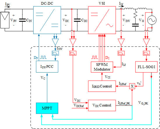
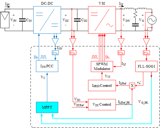
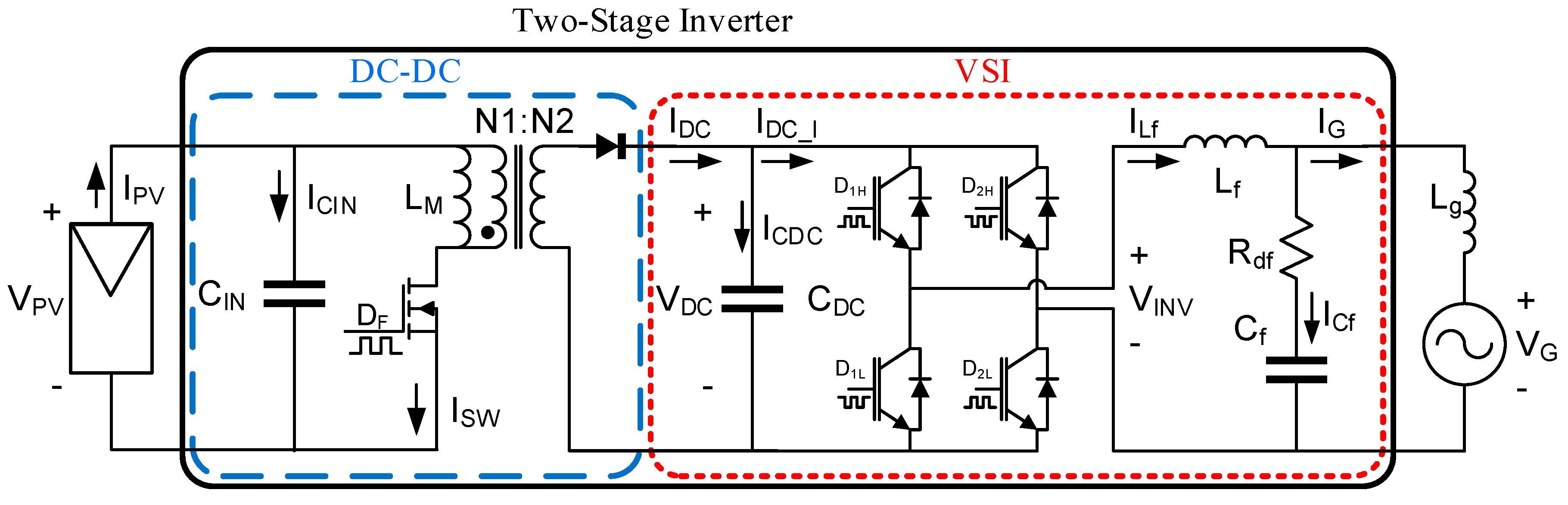
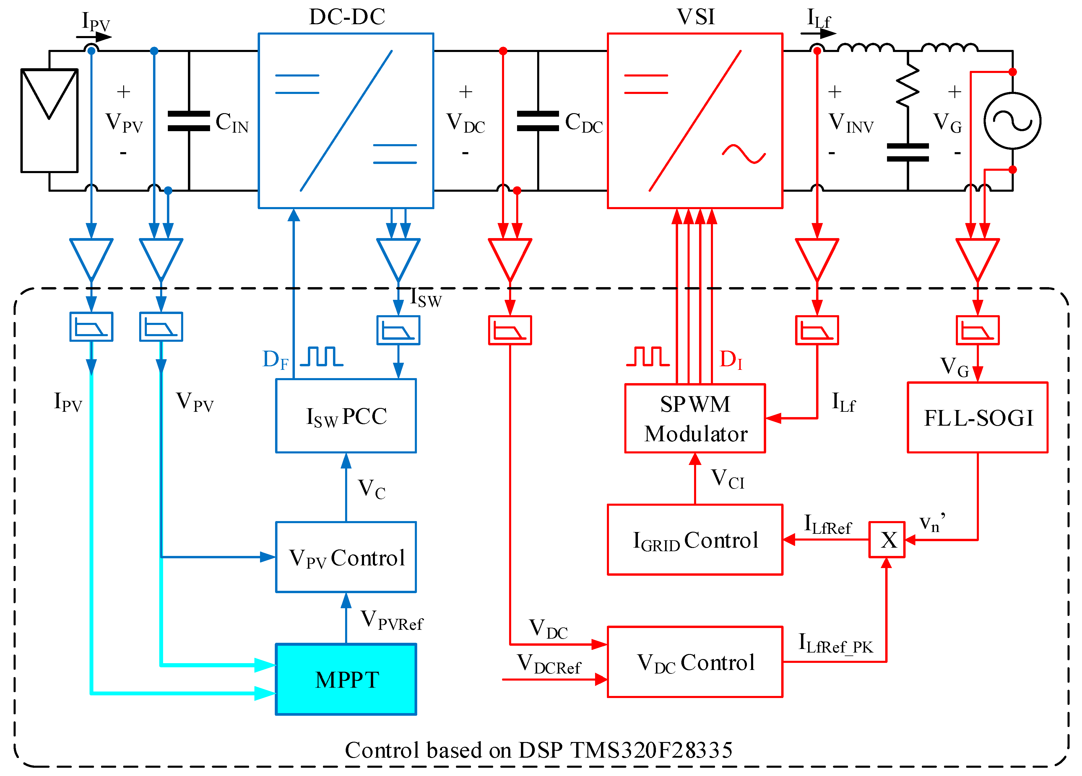
2. Two-Stage Grid-Connected PV Inverter

The two-stage grid-connected PV inverter shown in Figure 1 has been used for validating the theoretical study. It is formed by a flyback DC-DC and a single phase inverter. The inverter connects a single 230 W PV panel to the single-phase grid (230 Vrms, 50 Hz).
The inverter has a reduced size DC-link. Voltage and current sensors for the measurement of the PV panel voltage, VPV, and current, IPV, are available, in order to compare conventional MPPT algorithms, which make use of those sensors, with sensorless MPPT algorithms under the same conditions.
Costs saving associated with a smaller bulk capacitor and to the absence of MPPT sensors depends on several characteristics, but the estimation done for the implemented prototype is detailed in Table A1 of Appendix A.

2.1. Grid-tied VSI

The voltage source inverter (VSI) is formed by the DC-link capacitance (CDC), a full bridge of IGBTs and an LCL grid filter. The full-bridge is commutated by means of unipolar sinusoidal pulse width modulation (SPWM). The grid filter was designed following the guidelines of Reference [28]. The values of the inverter are shown in Table 1.
The current ICDC has high-frequency current components (IDC_SW) due to the switching of the transistors and a low-frequency current component (IDC_AC). The frequency of IDC_AC is twice the grid frequency and causes a voltage ripple at the DC-link (VDC_R). In Reference [18] it was shown that the minimum value of CDC is determined by the maximum and minimum permissible voltage at the DC-link caused by VDC_R. However, this criterion does not consider the dynamics of the DC-link [19] and transient voltage variations, that are due to changes in the operation point. The proposed value of the capacitance, CDC, to study the effects of a reduced DC-link is designed to limit the peak to peak value of VDC_R to 10% of VDC at nominal power (PG = 230 W), thus the value of the capacitance CDC is calculated following Equation (1).
C DC 2 · V G RMS · I G RMS V DC AV · π · F RDC · V DC R   PP = 230 V · 1 A 380 V · π · 100 Hz · 38 V = 50.7   μ F 50   μ F

2.2. Step Up DC-DC Converter

The DC-DC stage, shown in Figure 1, is a Flyback converter designed for boosting the voltage from the PV panel (VPV) up to the voltage of the DC-link (VDC) and providing high-frequency galvanic isolation between the PV panel and the grid. The converter is designed to work in discontinuous conduction mode (DCM) because the value of the transformer magnetizing inductance (LM) and the physical size of the transformer become smaller [15]. The MPPT algorithm establishes the operation point of this stage since the PV panel voltage is at the input of the DC-DC converter. It is worth pointing out that in the two-stage PV inverter structure the output voltage of the DC-DC converter is regulated by the inverter stage, whereas the panel voltage is controlled by the DC-DC converter following the reference value provided by the MPPT algorithm.
The current ISW, through the switch of the DC-DC converter, is composed by Equation (2) an average value equal to the PV panel current, IPV, and a high-frequency component, ICIN, provided by a low voltage input capacitance, CIN, following Equation (2).
I SW = I PV I CIN .
The size of CIN depends on the high-frequency current components at the input of the DC-DC converter. Besides, the value of the output capacitance, CDC, has an influence on the MPPT performance, since VPV is susceptible to the low-frequency voltage ripple at the DC-link voltage, VDC_R. It is worth pointing out that the implementation of a peak current control (PCC) is highly desirable for protecting the power switches from transient overcurrents. The values of the DC-DC converter are detailed in Table 2.

3. Control

The control of the two-stage inverter has been implemented digitally in a Texas Instruments TMS320F28335 [29] microcontroller with digital signal processor (DSP) extensions at a sampling frequency (FS) of 40 kHz. The controllers have been calculated in the continuous domain, having taken into account the digital delays, and then discretized using the bilinear “Tustin” transform. The delay between the sampling and the update of the reference inside the DSP has been done by using a second-order Padé approximation.
It is worth pointing out that the dynamic models used in this control study result from perturbing the averaged variables of the DC-DC converter or of the inverter stage around an operation point, as expressed by Equation (3). In Equation (3), X and x ^ denote the operation point value and the small-signal term of the averaged variable, x, respectively. The averaging is done in every cycle of the switching frequency.
x = X + x ^

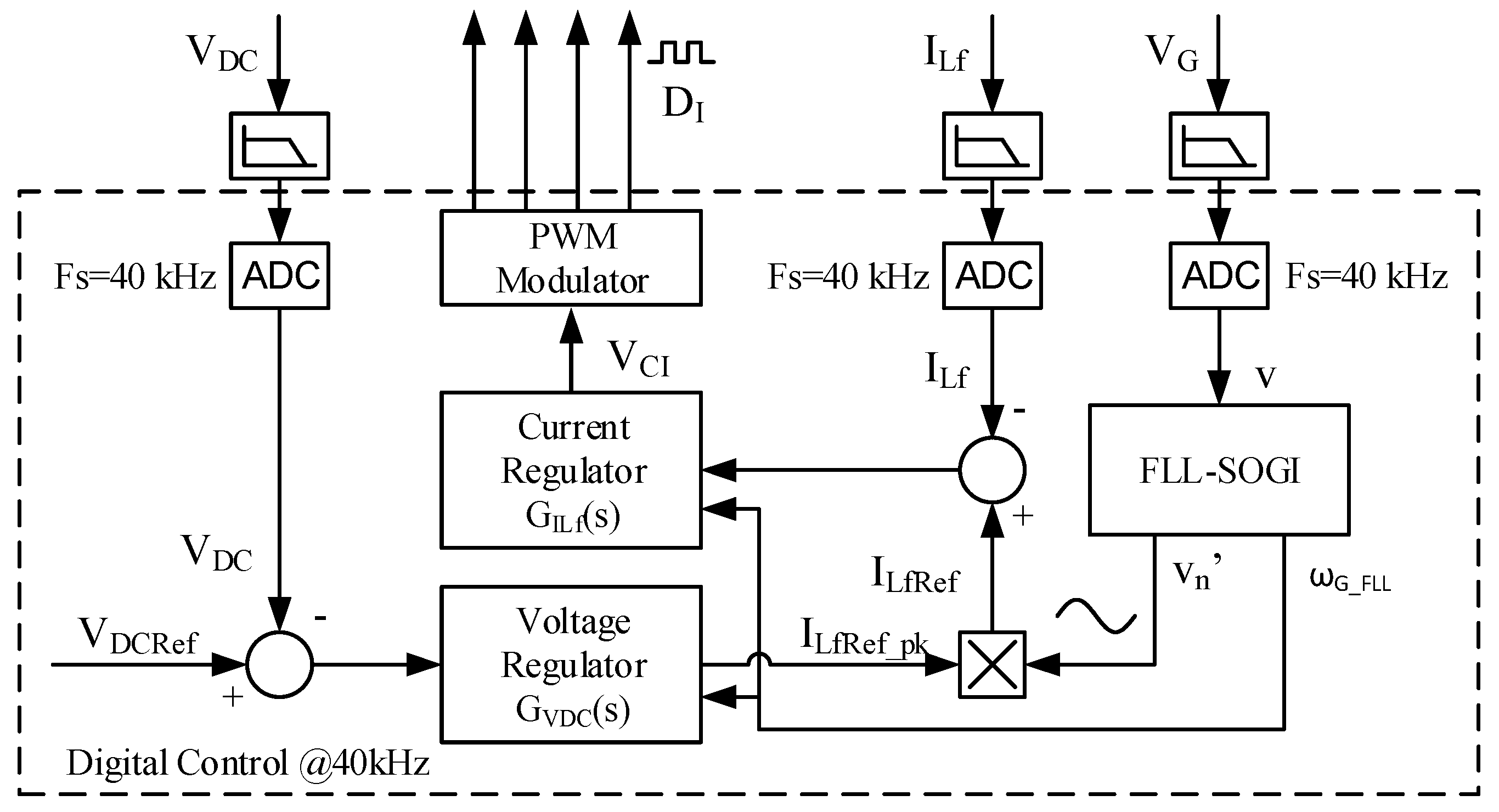
3.1. Control Scheme of the VSI Stage

The complete control structure of the VSI is shown in Figure 2.

3.1.1. Synchronization with the Grid

The synchronization with the grid voltage (VG) has been implemented by means of an SOGI based Frequency Locked Loop (FLL-SOGI) [27], which provides the calculation of the grid frequency in rad/s, ωG_FLL, a sinusoidal signal in phase with the grid, v’, and a sinusoidal signal in quadrature, qv’. The amplitude of the fundamental harmonic of VG, v’pk, is calculated following Equation (4), and a normalized sinusoidal signal in phase with the grid, v’n, is obtained in Equation (5).
v pk = v 2 + qv 2
v n = v v pk v n ( t ) cos ( ω G _ FLL · t )

3.1.2. Control of the Current Injected into the Grid

The control of the current injected into the grid, IG, is indirectly performed by controlling the current through the inductance Lf of the filter, ILf, because the control of ILf is less sensitive to grid impedance variations [30].
A proportional + resonant controller + a harmonics compensator (P + R + HC) current regulator, GILf(s), expressed by Equation (6), has been designed following Reference [26] and References [31,32,33,34] for tracking the sinusoidal reference of ILf, ILf Ref. Both the resonant and the harmonics compensator have been implemented by means of second-order generalized integrators (SOGI).
G ILf ( s ) = P Lf + R Lf ( s ) + HC ( s ) = K PLf + i = 1 , 3 , 5 , 7 K RLf [ i ] K BWRLf [ i ] · ( ω G _ FLL · i ) · s s 2 + K BWRLf [ i ] · ( ω G _ FLL · i ) · s + ( ω G _ FLL · i ) 2
Taking into account that the value of ωG_FLL used in Equation (6), provided by the FLL-SOGI, it can be concluded that GILf is adaptive in frequency, allowing high performance even under large variations of the grid frequency. The index ‘i’ in Equation (6) represents the corresponding harmonic. The gains of GILf are shown in Table 3.

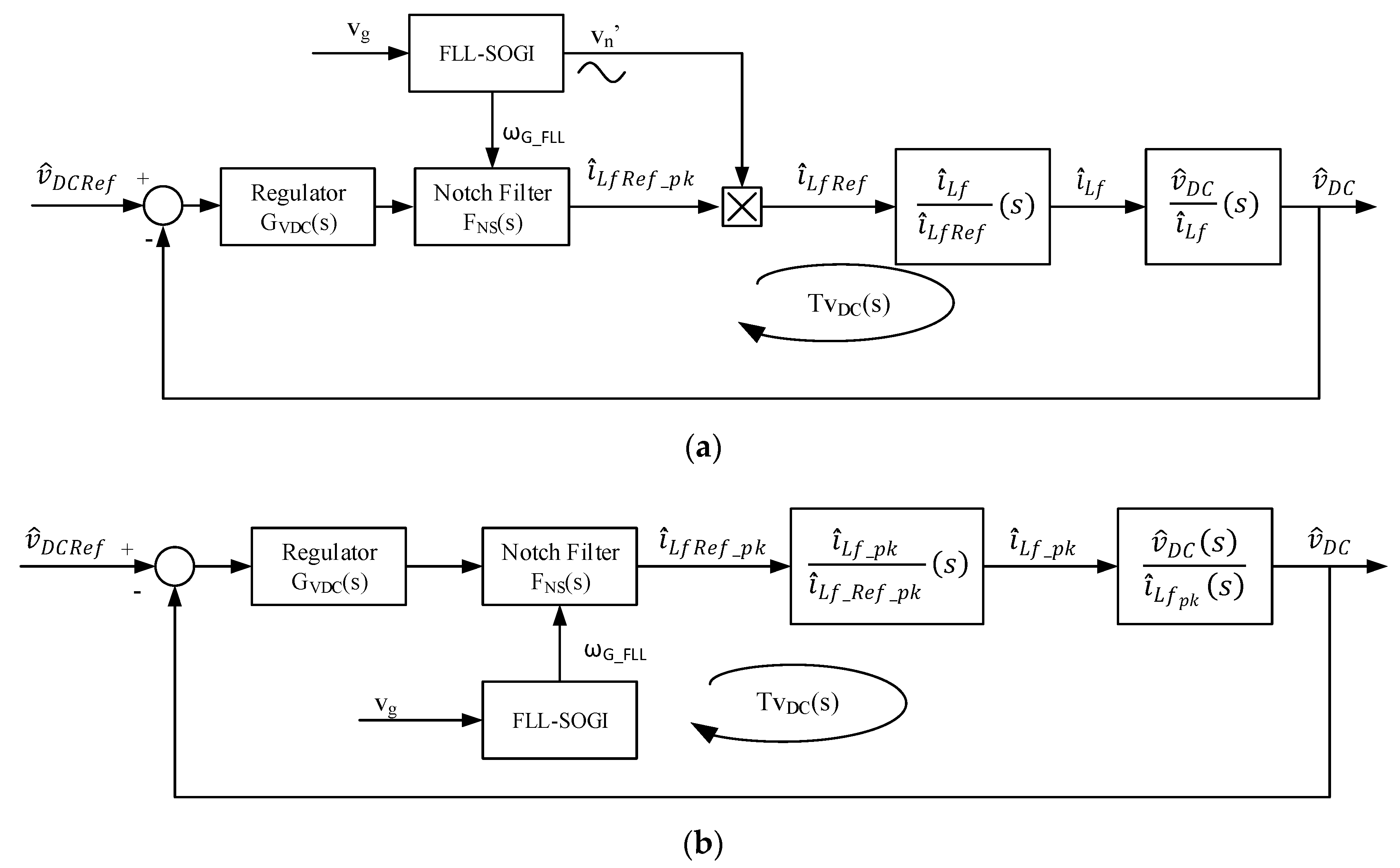
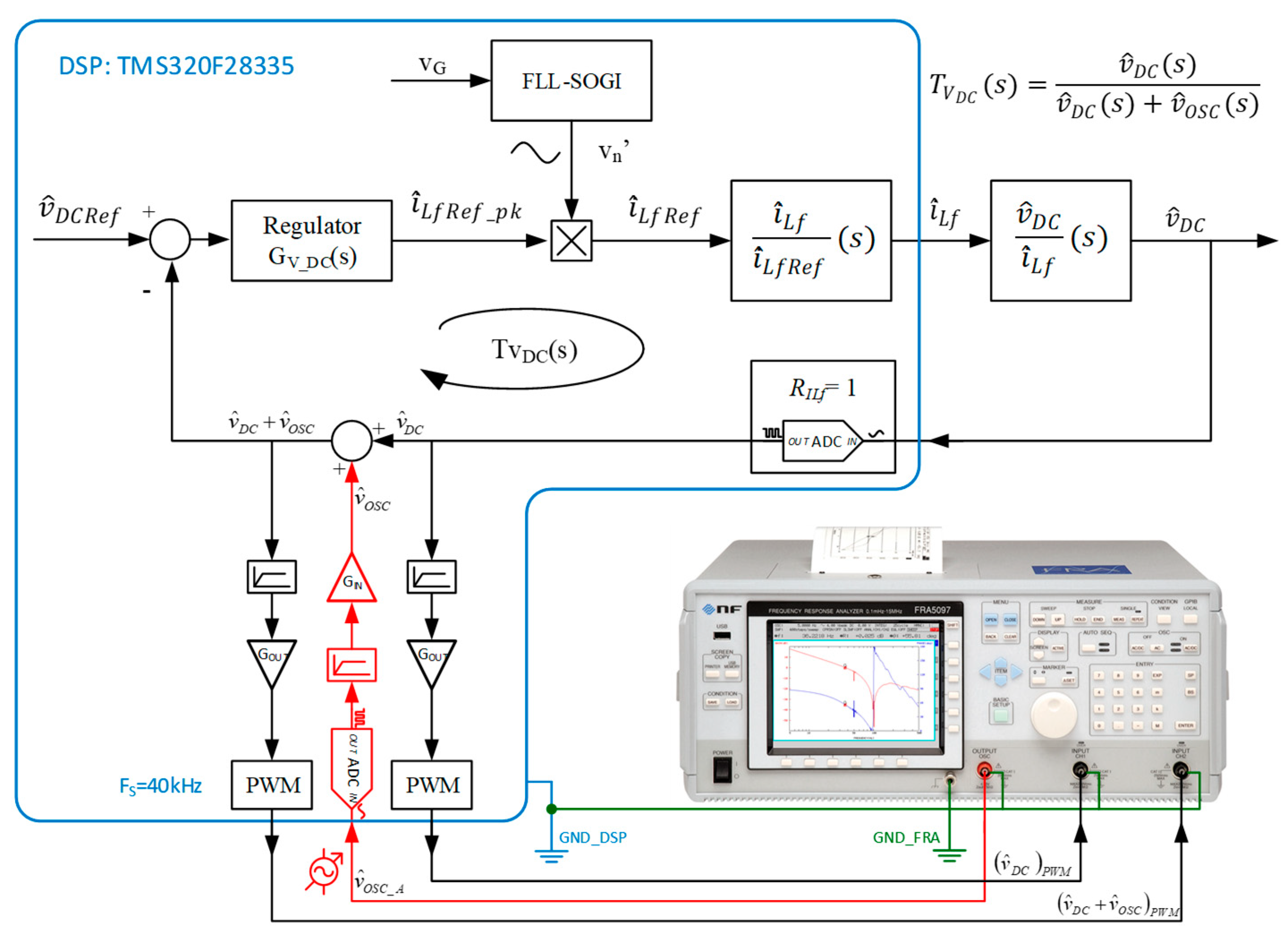
3.1.3. Control of the DC-link Voltage (VDC)

A reduced DC-link capacitance leads to the fast dynamics of the VDC control loop at the expense of an increase of the THDi of IG [16,17]. In Reference [16] a notch filter in the DC-link voltage control loop was implemented to reduce the low-frequency harmonics of IG. In the current study, the notch filter is implemented by means of SOGIs, achieving adaptation to grid frequency variations. This implementation allows an increase of the crossover frequency of the VDC control loop without increasing the distortion of IG, even with a high low voltage ripple at the DC-link and under large grid frequency variations. The control scheme of VDC is shown in Figure 3.
In Figure 3, two small-signal transfer functions play an important role. The first one is the transfer function i ^ Lf / i ^ LfRef ( s ) in Figure 3a, which is obtained by closing the control loop of ILf. This transfer function can be approximated by (7) in Figure 3b, where ωCi is the crossover frequency of the VSI current loop.
i ^ Lf _ pk i ^ Lf _ Ref _ pk ( s ) 1 1 + s ω Ci
In the case of a three-phase grid connected inverter, the derivation of the transfer function from the AC side active current to the DC-link voltage and the adjustment of the voltage loop PI regulator can be found in Reference [35], pages 210–219. In the case of the single-phase inverter under study, an analogous Equation (8) can be derived, based on the power balance and the power perturbation at the DC and AC sides. The transfer function from the peak value of the inverter output current at the AC side to the DC-link voltage can be expressed by Equation (8) after some derivation. Note that Equation (8) consists of a first-order transfer function with an (unstable) right half plane (RHP) pole, ωP_RHP, whose value depends on the operation point values VDC and IDC.
v ^ DC ( s ) i ^ Lf _ pk ( s ) = V G 2 · I DC 1 s ( I DC C DC · V DC ) = V G 2 · I DC 1 s ω P _ RHP ;   ω P _ RHP = I DC C DC · V DC
The loop gain TVDC(s) of Figure 3 is tuned by means of the PI regulator GVDC(s). Equation (9) provides the crossover frequency, Fc_VDC, one decade higher than ωP_RHP/(2 π). Note that an open loop unstable system can be stabilized by feedback only if the loop gain has a gain crossover frequency much higher than the maximum possible value of the unstable open loop pole, Fc_VDC >> ωP_RHP/(2 π) in this case. Besides, the value of Fc_VDC must be much lower than twice the grid frequency (FG), to reduce the effect of the low-frequency voltage ripple at the DC-link (fripple = 2 Fc_VDC) in the current reference signal iLf_ref, which could produce an unacceptable distortion of the grid injected current.
Gv DC ( s ) = 0.03902 · ( s + 0.6283 s )
It can be observed from Figure 3 that a notch filter, FNS(s), is placed in series with the PI controller GvDC(s). The expression of the notch filter transfer function is given by Equation (10). The center frequency of FNS(s) is twice the grid frequency (ωNS = 2 ωG_FLL) in order to filter the ripple at fripple coming from the sensed DC-link voltage. The tuning of the notch filter is provided by the FLL-SOGI previously described. The constant KNS is used to adjust the bandwidth of the filter, BWNS, as shown in Equation (11). The notch filter allows getting a high enough crossover frequency of the voltage loop with no distortion of the grid injected current. Note that a fast enough DC-link voltage loop is crucial to keep the DC-link voltage within safe values in reduced size DC-links with low capacitance.
F NS ( s ) = s 2 + ω NS 2 s 2 + K NS · ω NS · s + ω NS 2
BW NS · 2 π = K NS · ω NS K NS = 2 π · BW NS ω NS = 100 · 2 π 2 · F G · 2 π = 1
The Bode plots of TVDC(s) depicted in Figure 4a are those obtained when the notch filter, FNS(s), placed in series with GvDC(s) isn´t used. The PI regulator GVDC(s) (9) has been tuned in order to achieve a crossover frequency FC_VDC = 53 Hz, with a phase margin higher than 82° (PM > 82°) and a gain margin higher than 70 dB (GM > 70 dB). The system is stable but the attenuation at 100 Hz is just 5.5 dB. Therefore, the output of the voltage regulator has a remarkable low-frequency voltage ripple due to VDC_R, thus producing a high distortion of the grid current.
Figure 4b shows the Bode plots of TVDC(s) when the notch filter is used in series with GVDC(s). In that case the value of FC_VDC has slightly decreased (FC_VDC = 46 Hz), getting high stability margins: PM > 52° and GM > 70 dB. The system is also stable, but the attenuation at 100 Hz is higher than 100 dB.

3.2. Control Scheme of the DC-DC Stage

The control structure of the DC-DC stage is depicted in Figure 5. It is composed by an outer digital voltage loop, regulating VPV, in cascade with an analog peak current control (PCC) circuit, which sets the peak value of the current, ISW, through the Flyback converter power transistor.

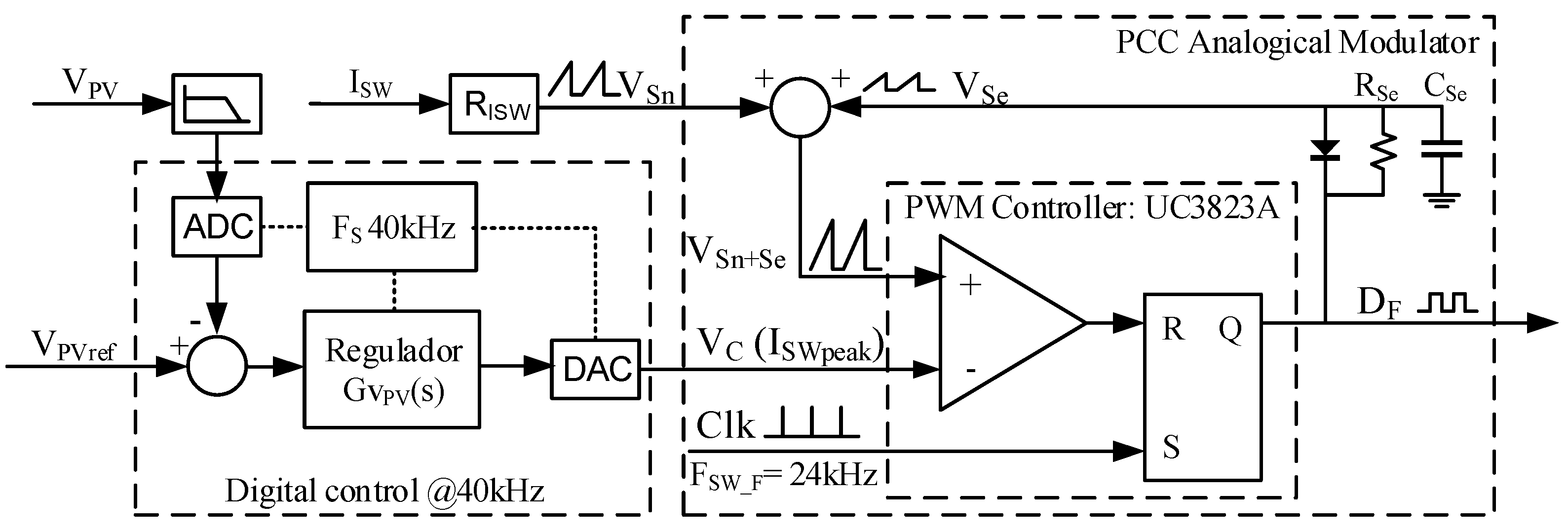
3.2.1. Peak Current Control of DC-DC Stage

The PCC control scheme shown in Figure 5 and has been designed following Reference [15]. This control structure is based on the cycle-by-cycle measurement of the current through the transistor, ISW, of the DC-DC converter. The peak value of ISW is limited by the control signal VC. An external stabilization ramp signal, VSe, is added to the sensed current signal, VSn. This method also provides protection for both the HF transformer and the power transistors against an eventual overcurrent.
The modulation index of the PCC, mc = 1 + Se/Sn (Equation (13)), is tuned by means of the slope Se of the external ramp VSe. The value Se = 110 V/ms accomplishes a dynamic behaviour of v ^ V PV / v ^ C ( s ) close to that of a first-order system, as it can be observed from Figure 6a. The high VDC_R ripple value produced by the low size of CDC can change the operation point along the I–V curve of the PV source, degrading the MPPT performance. Therefore, a low susceptibility of VPV to the ripple VDC_R is required. The open loop susceptibility of VPV to variations of VDC (Equation (14)) at 100 Hz is lower than −41.5dB as shown in Figure 6b, therefore VDC_R, that is 10% of VDC (40 Vpp), causes a VPV voltage ripple of 340 mVpp. It can be concluded that the 100 Hz ripple at VDC has a low influence on the PV voltage. Therefore, the sensing of VPV could be avoided and still a good MPPT would be obtained.
S N = R i V PV L m
F M = 1 ( S n + S e ) · T SW _ F = 1 m c · S n · T SW _ F
A ( s ) = v ^ V PV ( s ) v ^ DC ( s ) | v ^ C = 0

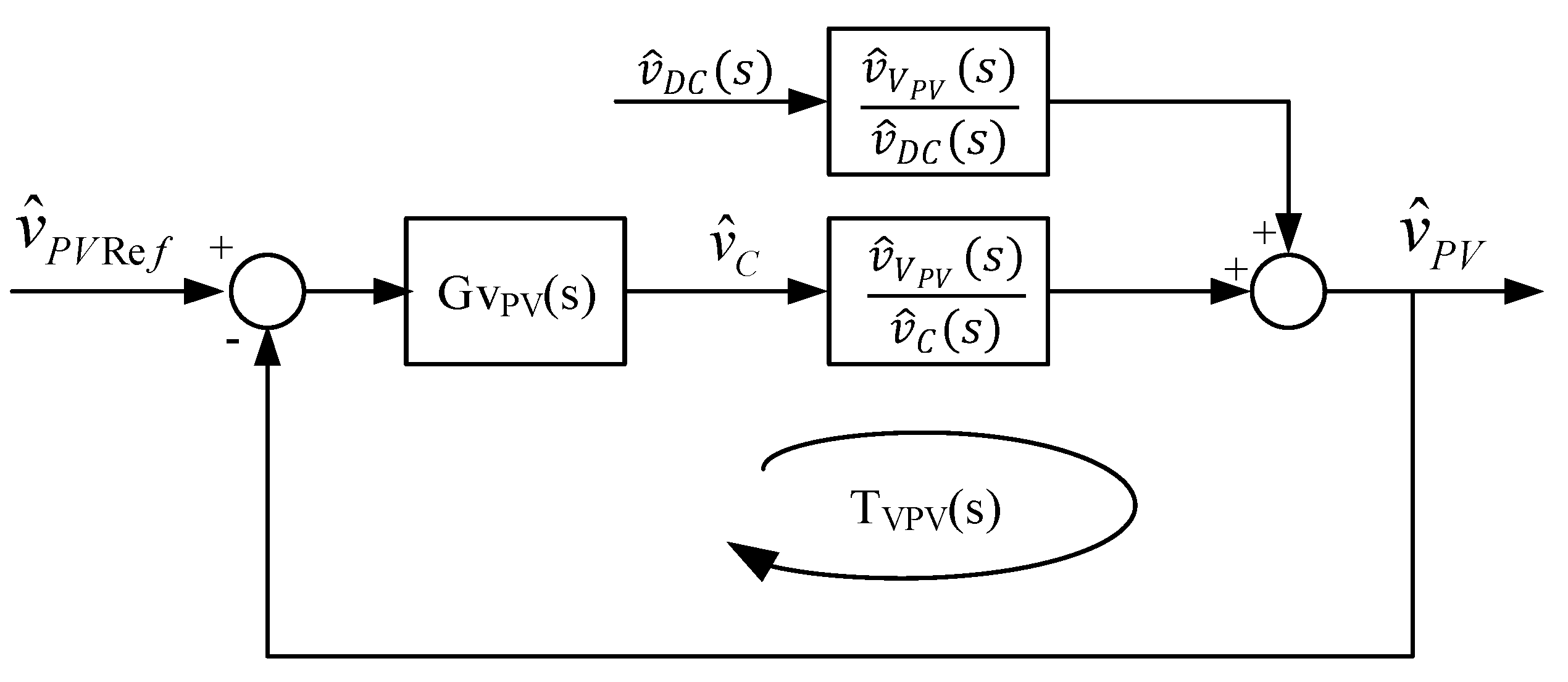
3.2.2. PV Panel Voltage (VPV) Control Loop in the Conventional MPPT

The reference of VPV (VPVRef) is updated at the sampling frequency of the MPPT, FMPPT. The PV panel voltage control loop is implemented digitally and its control scheme is depicted in Figure 7. The sampling frequency of the control loop (Fs) is 40 kHz. This control loop is adjusted by means the PI regulator GVPV(s), whose values are shown by Equation (15). The crossover frequency, FcVPV, of the loop gain TVPV(s) must be much higher than FMPPT so that VPV can track VPVref. The transfer function v ^ V PV / v ^ C ( s ) is the closed loop of the PCC and v ^ V PV / v ^ C ( s ) is the open loop susceptibility of VPV to the variations of VDC.
As it can be observed from the Bode plots of the loop TVPV(s) in Figure 8a, the crossover frequency FcVPV achieved by GVPV(s) is higher than 100 Hz. Therefore, an MPPT algorithm running at FMPPT = 10 Hz is suitable Figure 8b shows that the presence of this control loop reduces the susceptibility v ^ V PV / v ^ DC ( s ) (16) at 100 Hz down to −55 dB, therefore the voltage ripple in VPV caused by VDC_R is 71 mVpp. Note that the use of a control loop of VPV reduces the sensitivity of VPV to the 100 Hz ripple in VDC in a factor of around 5: The ripple in VPV is 71 mVpp with voltage loop compared with 340 mVpp with only PCC loop.
G VPV ( s ) = 1.8345 ( s + 350 s )
A CL ( s ) = v ^ PV ( s ) v ^ DC ( s ) | v ^ PVRef = 0

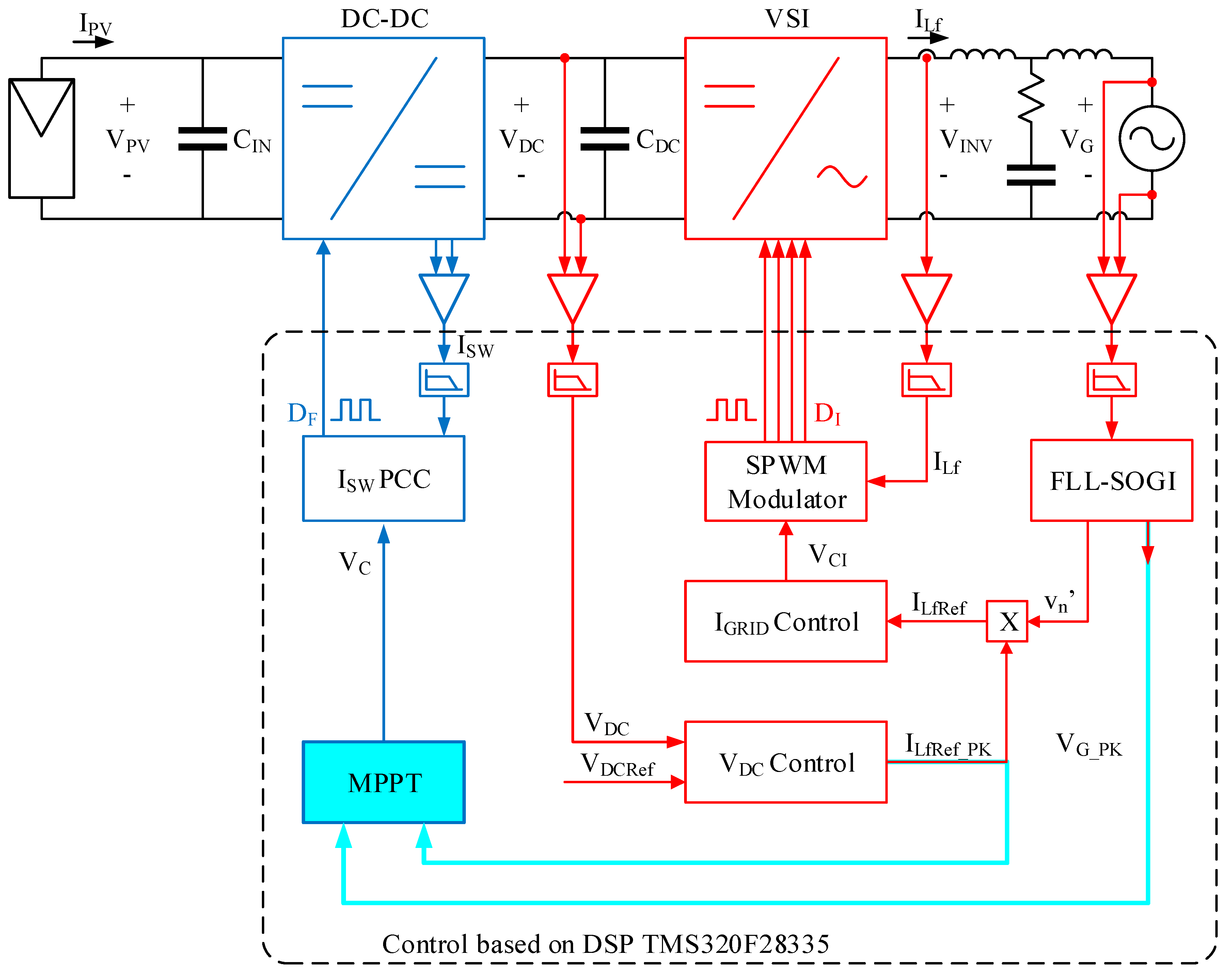
4. MPPT Implementation without VPV and IPV Sensors

The conventional implementations of MMPT algorithms use current and voltage sensors to measure the voltage (VPV) and the current (IPV) of the PV source as it is shown in Figure 9. The use of voltage and current sensors increases the cost of the power converter. Sensorless MPPT algorithms have been developed [10,11,12,13] in order to reduce the number of sensors, yielding a cost reduction. In [11] a sensorless MPPT implementation based on the power balance at the DC-link was presented, which relies on the fact that the power injected into the grid (PG) can be considered almost equal to the power extracted from the PV panels, PG ≈ PPV. In that implementation, the reference of the current injected into the grid (IG) is used as an estimation of PG. This reference current depends on the control loop of VDC so that the sampling frequency of the MPPT algorithm (FMPPT) is limited by the dynamics of that loop. Besides, the reference of IG is sensitive to the variations of the grid voltage and has a low-frequency ripple due to VDC_R. Moreover, the method explained in Reference [11] is based on the assumption that the amplitude of the grid voltage is stable.
A sensorless MPPT implementation shown in Figure 10 is proposed in this work. In this implementation, there is neither VPV nor IPV sensors and it is assumed that the power injected into the grid is almost equal to the power extracted from the PV panels, PG ≈ PPV, as in Reference [11]. A novelty of this research is that it takes de advantages of the PCC of the DC-DC stage and some SOGI based enhancements applied to the control of the VSI stage to improve the performance of the MPPT implementation.
A perturb and observe (P and O) algorithm [36] has been programmed in both the conventional (Figure 10) and the proposed sensorless (Figure 11) MPPT algorithms to compare the performance of both implementations. Both implementations use the grid frequency as a time-base to execute the MPPT algorithm. This technique increases the rejection of the disturbances caused by VDC_R. In previous applications of a similar technique [12], the MPPT algorithm was executed at twice the grid frequency, but that sampling frequency is too fast for the control loops implemented in the proposed sensorless algorithm. In the present study, the MPPT algorithm was executed once every five cycles of the grid, yielding FMPPT = 10 Hz.
In the conventional implementation, the MPPT algorithm provides the reference of VPV (VPV_Ref) to the VPV control loop. In the proposed sensorless MPPT, both the VPV sensor and the VPV control loop have been removed, so that the MPPT provides the reference Vc to the analog PCC.

4.1. Estimation of the Power Injected into the Grid in the Sensorless MPPT

The reference ILf_Ref_PK is the peak value of the current injected into the grid, being proportional to PG when the amplitude of the grid voltage is a static value. The signal ILf_Ref_PK may have a remarkable low-frequency voltage ripple due to VDC_R, thus producing a high distortion of the grid injected current along with a disturbance in the estimation of PG. The SOGI based notch filter FNS(s) in series with the regulator GVDC(s) shown in Figure 3 is used to filter out that ripple. The use of the notch filter also enables a high crossover frequency of TVDC(s) without increasing the ripple in ILf_Ref_PK, which is useful to implement a fast MPPT algorithm. The crossover frequency of TVDC(s) is FC_VDC = 45 Hz so that an MPPT of FMPPT = 10 Hz can be implemented.
The estimation of PG, PG_est, depends on IG and on the grid voltage RMS value (VG) so that variations of VG perturb the calculations of PG_est. To overcome this issue, the value of the signal v’pk is used to calculate the estimation of PG as it is shown in Equation (17). The signal v’pk is the amplitude of the fundamental of VG and is provided by the FLL-SOGI, not requiring additional computational resources. The signal v’pk has very low sensitivity to the distortion of the grid voltage because it is naturally filtered by the FLL-SOGI.
P G _ est = v pk 2 · I LfRef _ PK 2 = v pk · I LfRef _ PK 2 P PV

4.2. Implementation of the Perturb and Observe (P&O) Algorithm
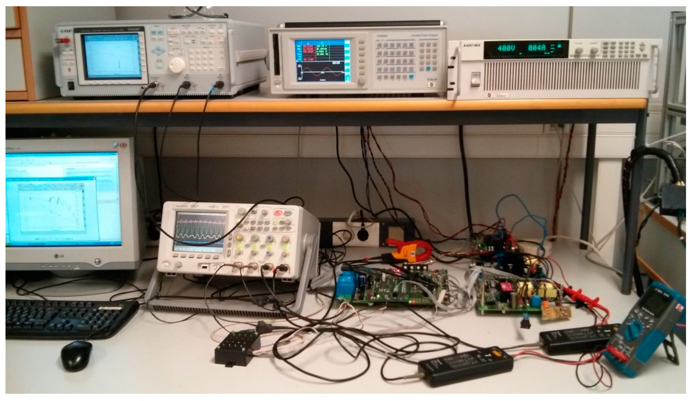
The conventional MPPT algorithm uses the measurements of VPV and IPV to set the operation point of the PV source. The algorithm increases or decreases VPV_Ref in perturbation steps of a value ∆VPV_Ref to move the operation point along the I–V curve. In the sensorless implementation shown in Figure 10, instead of the measurements of VPV and IPV, the value of PG_est expressed by Equation (17) was used. In Reference [11] it was proposed to manage the duty cycle of the switches (DF) of the DC-DC to move the operation point along the I–V curve. In inverters with a reduced DC-link, the high susceptibility of VPV to the ripple VDC_R disturbs the operation point in the PV panel.
In the proposed sensorless MPPT, the value of IPV is indirectly set by means of the reference signal of the PCC loop, Vc. The use of PCC has two functions: reducing the susceptibility of VPV to the ripple VDC_R and protecting the DC-DC converter from overcurrents.
The variable Vc is increased or decreased in small steps of a value ∆Vc. It is worth pointing out that an increase of Vc causes an increase of IPV, moving the PV operation point to the left of the I–V curve, whereas a decrease of Vc moves the PV operation point to the right of the I–V curve.

5. Results

Figure 11 depicts the experimental setup. The laboratory tests have been performed using the two-stage inverter presented in Figure 1. The inverter under test was designed for connecting a single PV panel of 230 W to the single phase grid (230 VRMS @ 50 Hz) and has a DC-link with the capacitance calculated in (1), CDC = 50 µF. The challenge of using such a small value of CDC is to keep a low distortion of the grid current and small transient overvoltages at the DC-link. The control of the two-stage inverter has been implemented digitally in a Texas Instruments TMS320F28335 DSP [30] at a sampling frequency (FS) of 40 kHz.
The grid was emulated by means of a Cinergia GE&EL 50 grid emulator and electronic load. The voltage waveform was programmed according to the test waveform described in the international standard IEC-61000-4-7 [37], which has a value: THDV = 1.2%. The PV panel has been emulated by means of an AMETEK TerraSAS ETS1000X10D PV simulator.

5.1. Control of the VSI

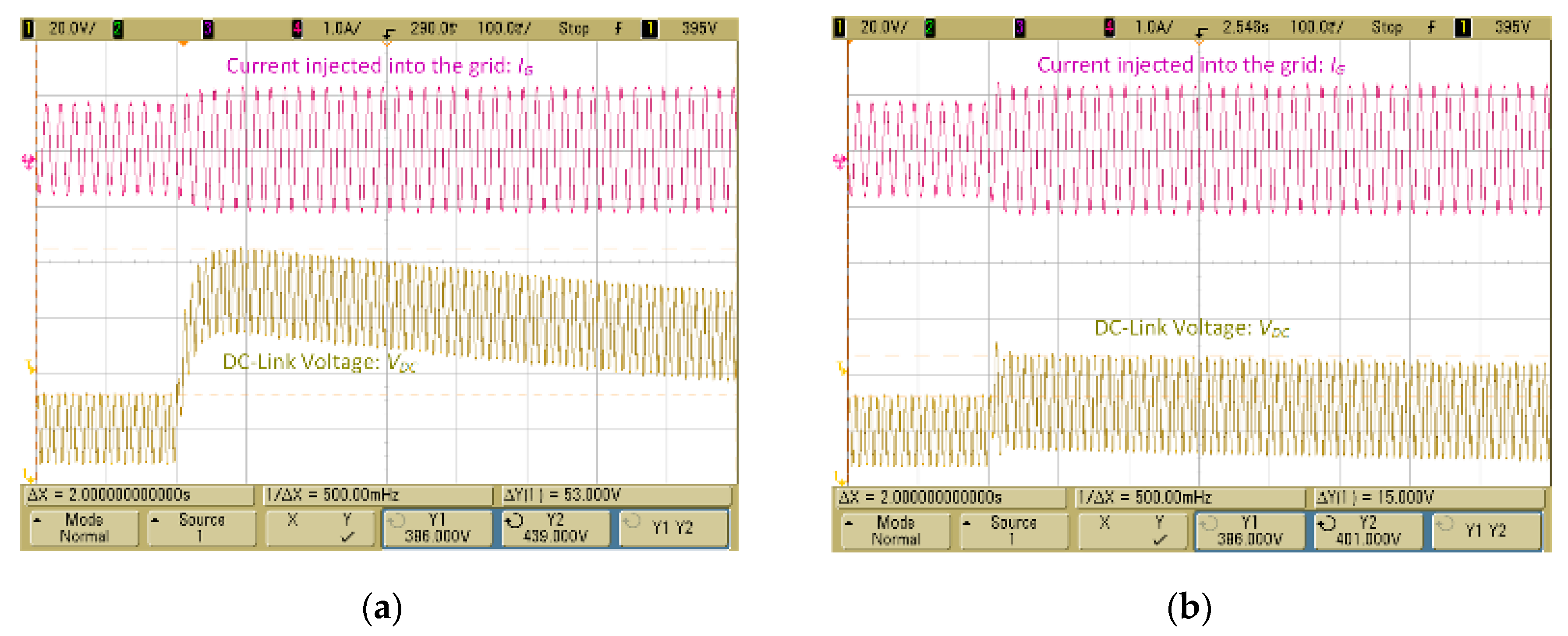
5.1.1. Transients of the DC-link Voltage

Figure 12 shows the transient response of the DC-link voltage (VDC) and the current injected into the grid (IG) when the PV power steps from 150 W up to 200 W. The results shown in Figure 12a were obtained with a crossover frequency Fc_VDC = 10 Hz, yielding an overvoltage in VDC of 53V from its steady-state value. The response in Figure 12b is obtained with a crossover frequency Fc_VDC = 45 Hz. The response in Figure 12b was close to five times faster and the overvoltage is only 15 V, which represents a reduction of 72%.

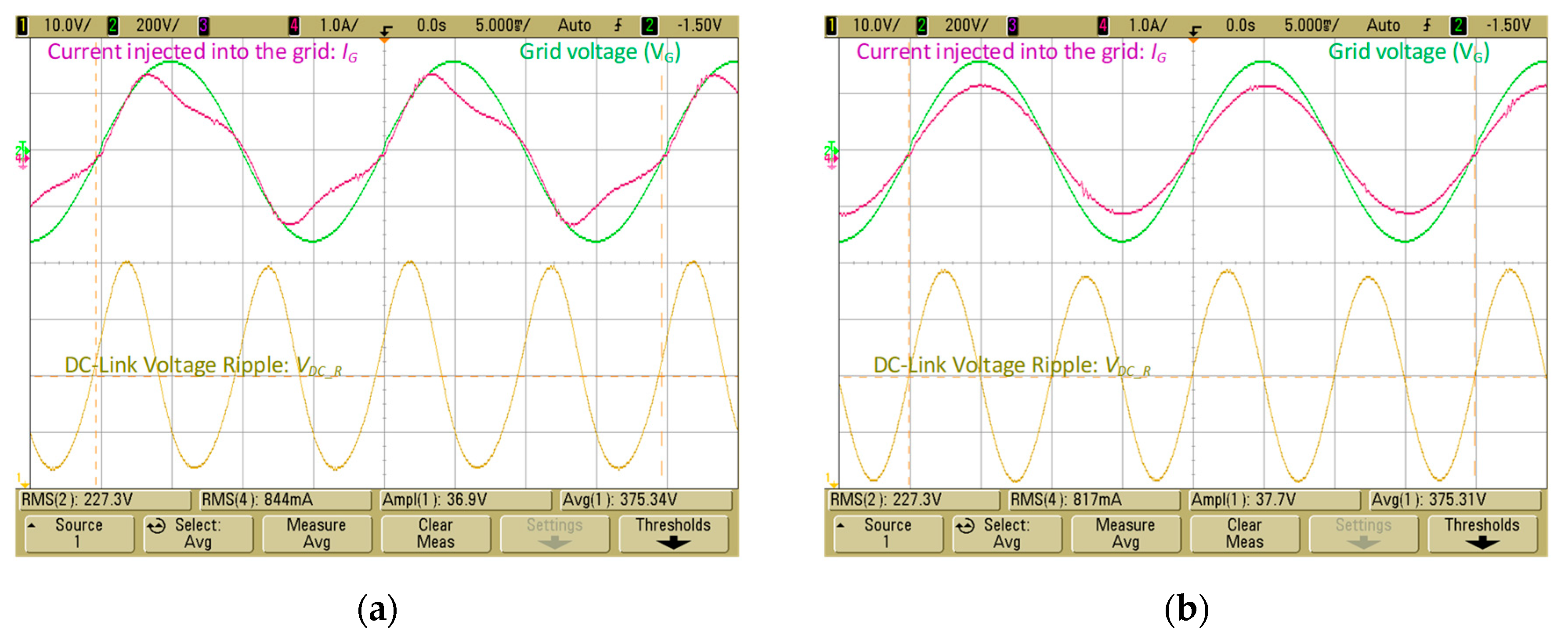
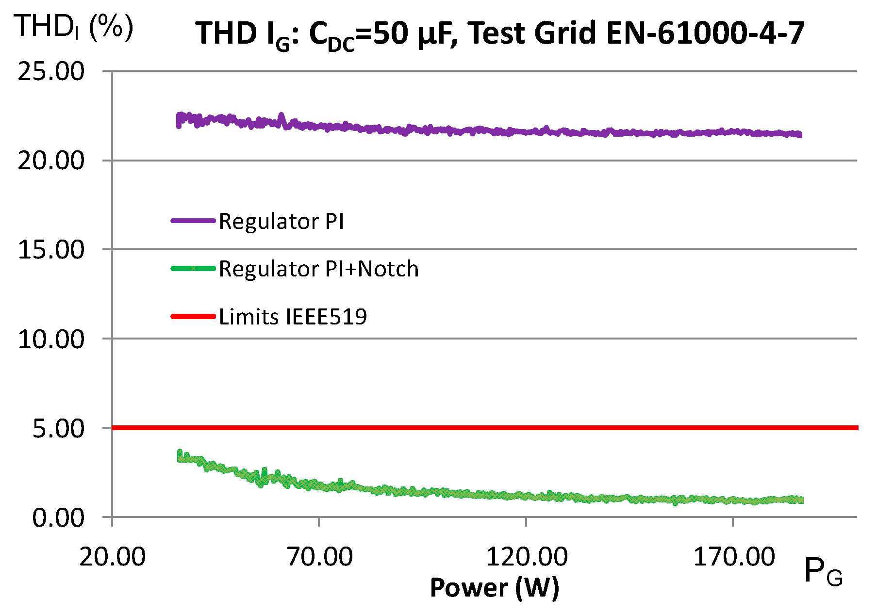
5.1.2. Influence of the SOGI Notch in the Distortion of the Current Injected to the Grid

The increment of the crossover frequency Fc_VDC involves a higher susceptibility to VDC_R, which increases the harmonic distortion of the current injected into the grid (THDi). Figure 13 depicts the current injected into the grid (IG) using two different regulators for controlling VDC. In Figure 13b, the regulator GVDC(s) of the VDC control loop is the PI shown in Equation (9) with a crossover frequency Fc_VDC = 53 Hz. The waveform of IG in Figure 13b was obtained using the same PI regulator, but in series with the SOGI notch filter FNS(s) shown in Equation (10), centered at 100 Hz. The crossover frequency has been slightly reduced, Fc_VDC = 45 Hz, taking into account the addition of FNS(s).
Both tests have been performed injecting 200 W to the grid. The controller of the current injected into the grid (IG) is formed by the P+R regulator in series with the HC expressed by Equation (6). The resulting values of the THDi are 21.51% and 0.96%, respectively. This result indicates the effectiveness of the notch filter for reducing the THDi in spite of the small DC-link.
The following tests of the THDi have been performed for values of PG in the range PG = [40, 180] W. The results are shown in Figure 14. The purple trace represents the values of THDi obtained without the SOGI notch FNS(s) and the green trace represents the values obtained with FNS(s). The THDi without notch varies from 21.51% to 22.43%, clearly exceeding the limits of the IEEE519 standard [4] (5%), shown by the red line. The values of the THDi obtained with FNS(s) vary from 0.96% to 3.14%, widely complying with IEEE519 in the whole range of PG values. In all the measurements the distortion of the grid voltage is THDv = 1.2%.

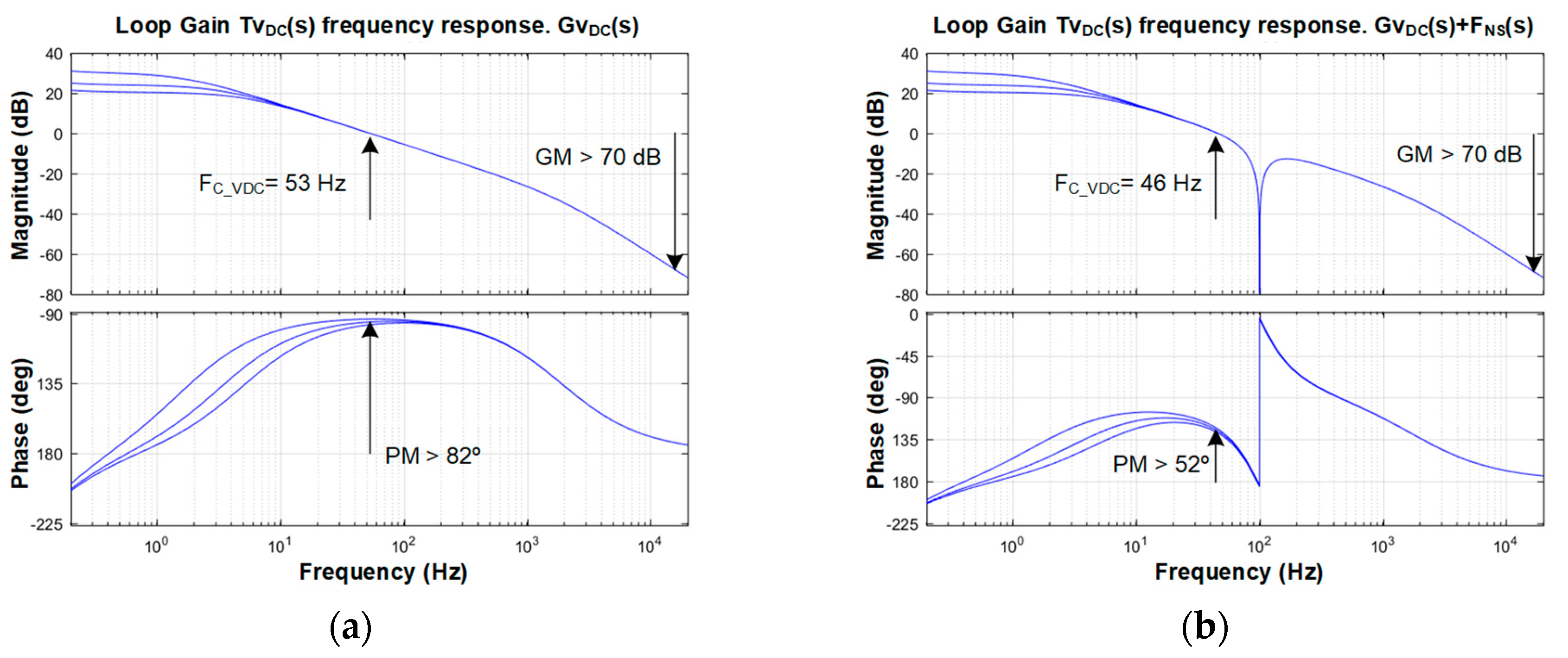
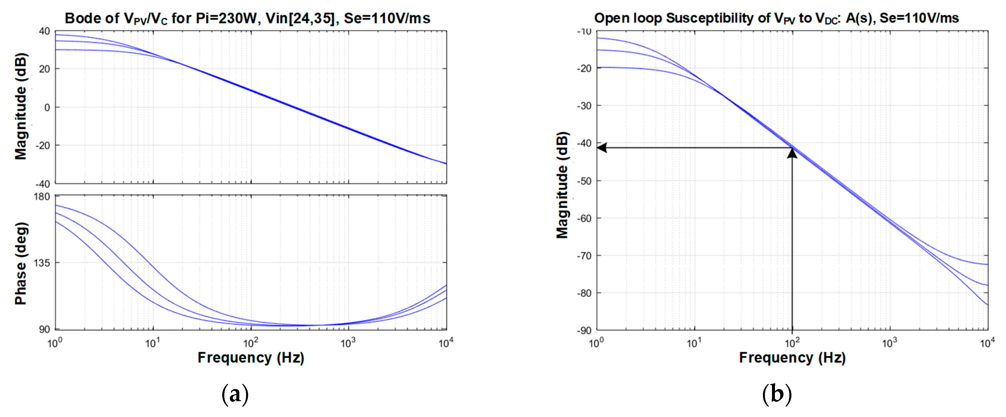
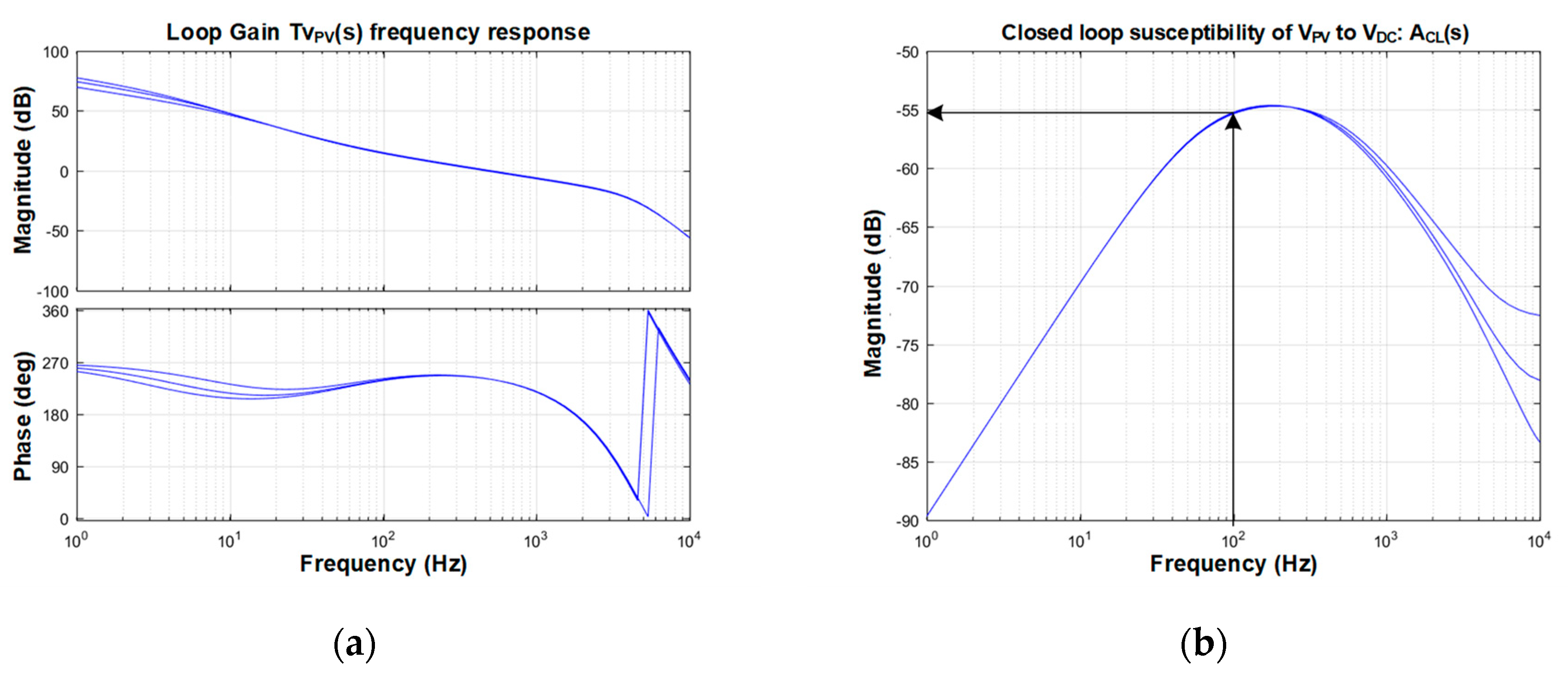
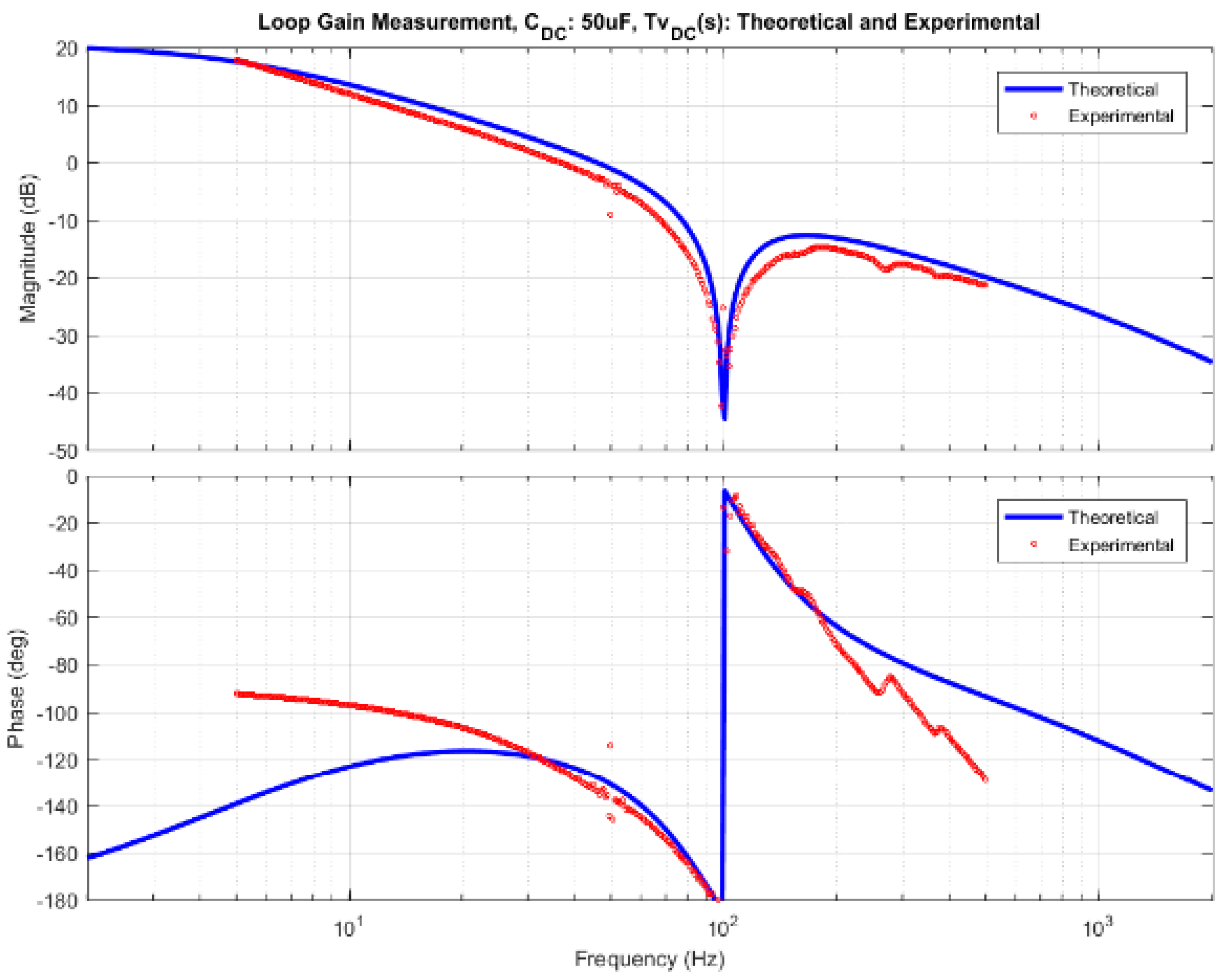
5.1.3. Loop Gain Measurement

The loop gain TVDC(s) has been validated by means of loop gain measurement procedures [38,39,40]. The setup of the test is shown in Figure 15. An NF FRA5097 frequency response analyzer (FRA) is configured to perform an AC sweep from 2 Hz to 20 kHz. The signal generated by the oscillator of the FRA (vOSC_A) is acquired by the DSP, which carries out the control of the inverter through an internal 12-bit ADC. The acquired signal (vOSC) was digitally injected into the control loop as a perturbation. Both, vDC and vDC+vOSC signals were adapted digitally to be loaded into the pulse width modulation (PWM) unit of the DSP. The offset of the signals was removed through digital high pass filters, and then the amplitudes are digitally adjusted to maximize the resolution of the PWM. The PWM signals (vDC)PWM and (vDC + vOSC)PWM were measured by the FRA. The PWM signals were filtered by the FRA through its internal tracking filter. The loop gain measurement of TVDC(s), shown in Figure 16,was performed at PG = 230 W. The results show the similarity between the experimental and theoretical Bode plots of TVDC(s).

5.2. MPPT

The performance of the sensorless “perturb and observe” (P and O) MPPT algorithm presented in this study has been compared to a conventional implementation, which uses sensors to measure VPV and IPV. The experimental tests have carried out to measure the start-up time until the maximum power point (MPP) was reached, and the performance at the MPPT under irradiation transients. All the tests were performed with an MPPT sampling frequency, FMPPT = 10 Hz. The perturbation step value programmed in the conventional implementation was ∆VPV_Ref = 300 mV. In the sensorless MPPT the perturbation step was ∆Vc = 12.5 mV, which corresponds to a 250 mA step in IPV in the operation region close to the MPP. It is worth pointing out that different values are perturbed in both MPPTs (either VPV_Ref or ∆Vc) and that the DC-DC converter operates in discontinuous conduction mode. Both facts prevent finding an equivalent value of the perturbation step in both MPPTs.

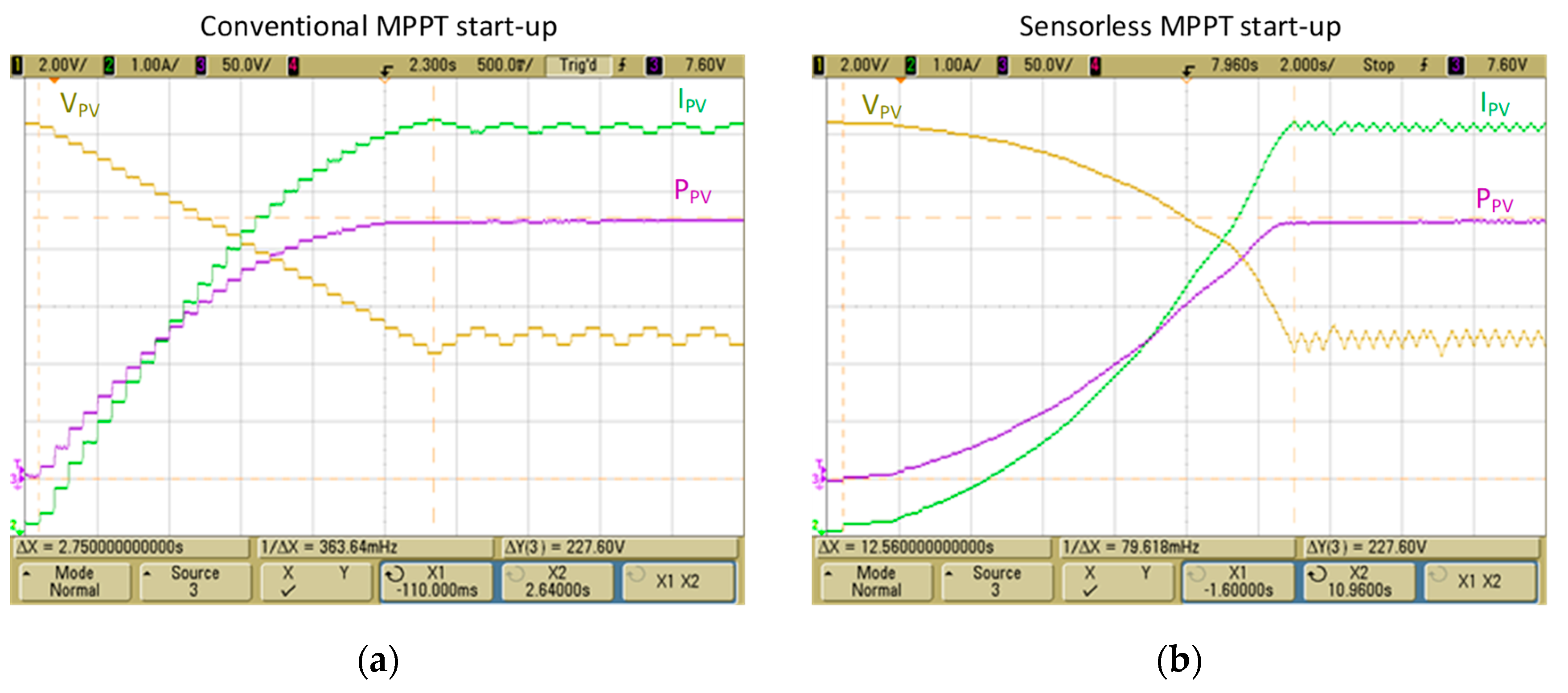
5.2.1. Start-up Time to Reach the MPP

Figure 17 shows the evolution of the operation point at the PV source (VPV, IPV and PPV) from the start-up until the MPP was reached. The conventional implementation was faster (2.75 s) than the sensorless (12.6 s) due to the differences in the perturbation step, but once the MPP is achieved, both implementations continue at the MPP.

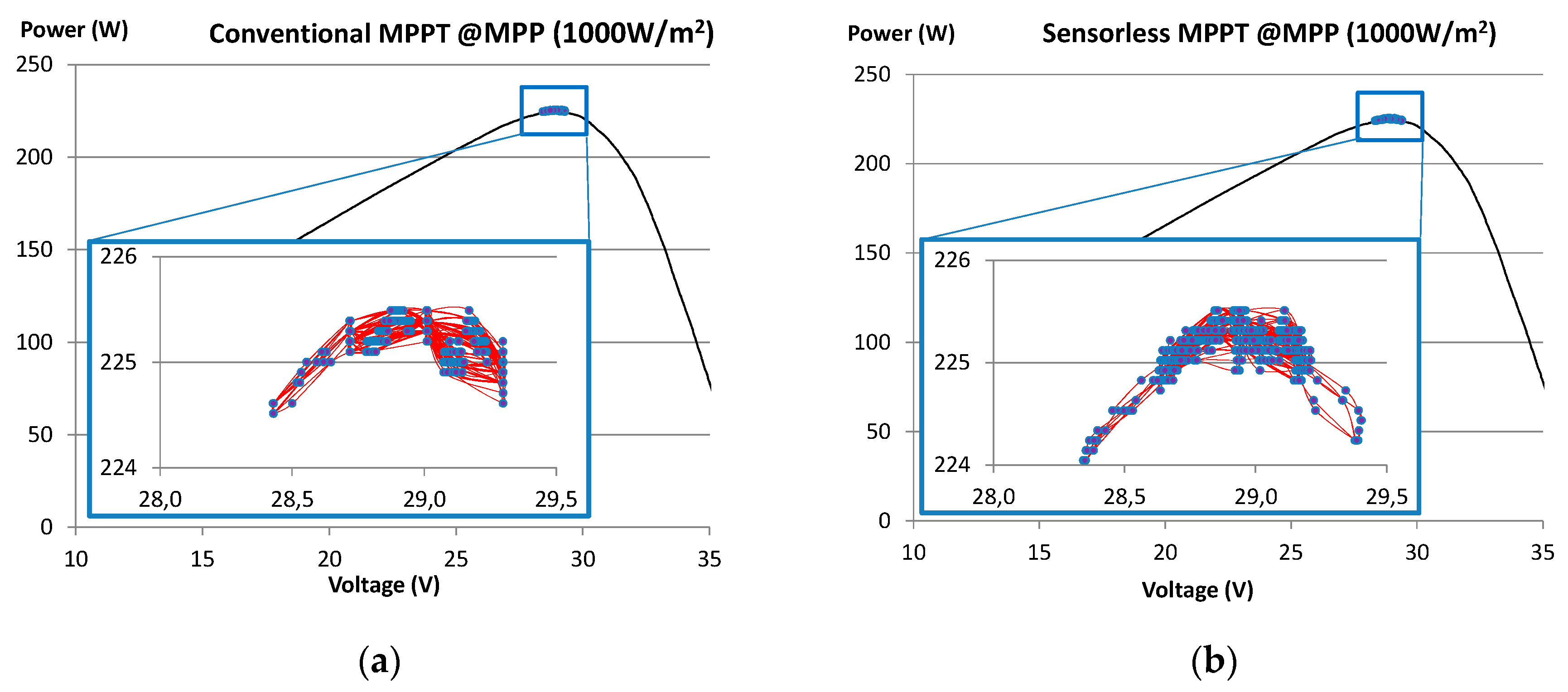
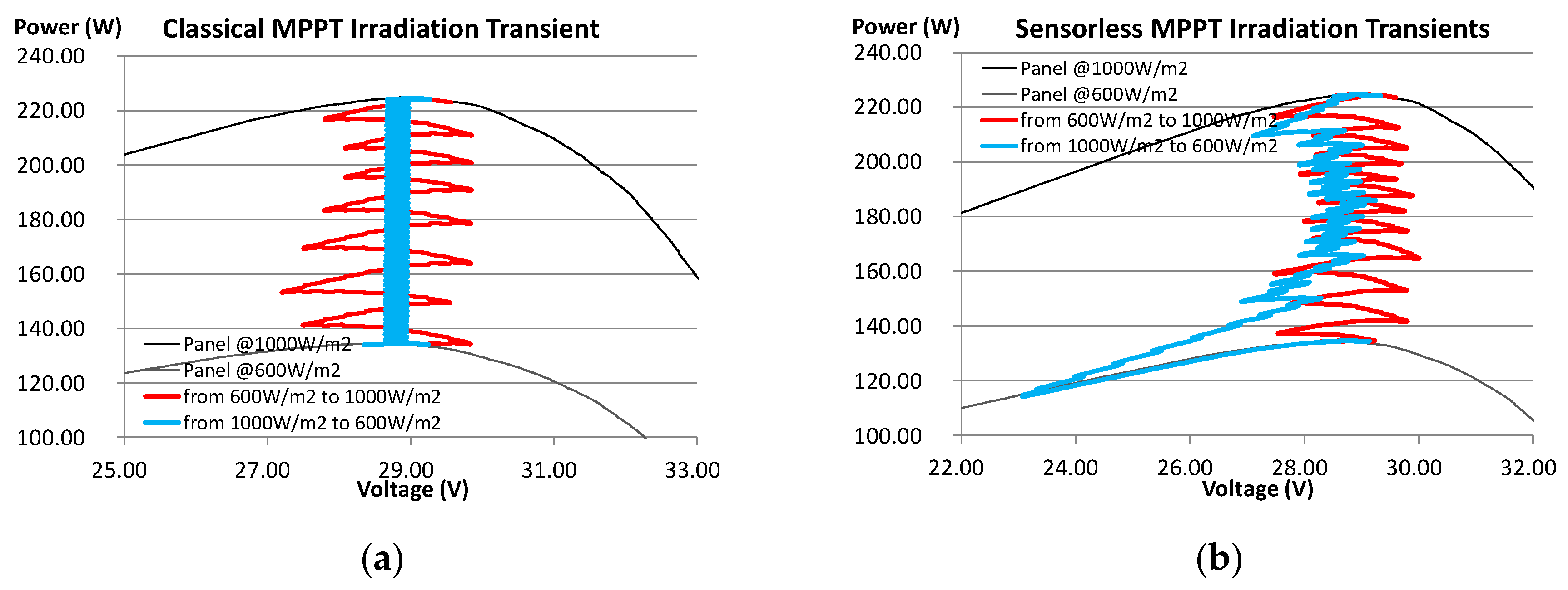
5.2.2. MPPT Performance Close to the MPP

A key factor in the MPPT performance is the accuracy of the PV estimation and the dispersion of the operation point from the MPP along the I–V curve. The results shown in Figure 18 were obtained tracking the MPP of the 230 W PV panel at constant irradiation of 1000 W/m2 during 50 s. The results in Figure 18a correspond to the conventional MPPT algorithm and the results in Figure 18b correspond to the sensorless algorithm. In both implementations, the operation points are very close to the MPP. The power extracted from the PV panel during the tests is shown in Table 4. In order to calculate the MPP tracking performance, the quotient between the average power and the peak power measured in each experiment has been used as a reference, as it is expressed by Equation (18). Although the sensorless algorithm presents a very slight disadvantage (0.06%) in terms of the tracking efficiency, the performance of both methods is almost the same.
Tracking   efficiency = Average   Power Peak   Power .
The tracking of the MPP under heavy irradiation transients is shown in Figure 19. The tests have been performed for 50 s following the stages shown in Table 5. The black traces are the IV curve of the PV panel at 1000 W/m2 and 600 W/m2. The blue traces represent the evolution in stage 2, during the reduction of the irradiation, and the red trace represents the evolution in stage 4, during the increase of irradiation.
The power extracted from the PV panel during the tests is shown in Table 6. During stages 1, 3 and 5, both MPPTs tracked the MPP as was expected from the results shown in Table 4. During stage 2, the sensorless MPPT was not as accurate as the conventional one, but during stage 4 the sensorless MPPT exhibited a smaller dispersion of the operation point and, thus, a higher accuracy than the conventional one. It can be stated that the MPPT performance of both MPPTs was highly similar. Although the conventional MPPT had a faster start-up and was slightly more accurate in some tests, the performance of the proposed sensorless MPPT near the MPP was almost equal to the conventional implementation, but at a lower cost.

6. Conclusions

This paper focused on control techniques which help to reduce the cost of two-stage grid-connected PV inverters. In previous works, sensorless algorithms and techniques to reduce the capacitance of the DC-link have been proposed separately. The present study attempts to integrate both trends in a single implementation. The reduction of the DC-link capacitance requires a faster control loop to keep the DC-link voltage within safe values. However, this practice usually increases the THD of the current injected into the grid. The DC-link can be reduced in a factor of ten compared to standard values of the DC-link capacitance, yet with good values of the THDi, by increasing the speed of the voltage control loop and using a frequency adaptive notch filter tuned at twice the grid frequency.
SOGI structures are an effective way to implement tuned filters both in the inverter voltage loop and in its current loop. It is shown that the crossover frequency of the DC-link voltage control loop can be increased from typical values of 10 Hz to a value around 50 Hz, yet getting a THDi value lower than 1%. The combination of a fast voltage loop with a SOGI notch filter allows the reduction of the DC-link capacitance. An FLL-SOGI is used to get the value of the grid frequency to tune the SOGI controllers in the inverter control loops.
Summing up, this study proposes the implementation of the MPPT with no sensors at the PV source side, which takes advantages of the SOGI based enhancements implemented in the control of the converter. The high dynamics achieved by the inverter controllers yield a performance of the sensorless MPPT very similar to that of conventional MPPT implementations, but at a lower cost.

Author Contributions

R.G.-M., G.G. and E.F. proposed the main idea, performed the investigation and designed the experiments; R.G.-M. and G.G. developed the software, performed the experiments, and wrote the paper. M.L. and S.M. processed the data from the experimental results and reviewed the paper. G.G. and E.F. lead the project, acquired the funds for research.

Funding

This work has been co-financed by the Spanish Ministry of Economy and Competitiveness (MINECO) and by the European Regional Development Fund (ERDF) under Grant ENE2015-64087-C2-2-R and by the Spanish Ministry of Science, Innovation and University (MICINN) and the European Regional Development Fund (ERDF) under Grant RTI2018-100732-B-C21. The European Regional Development Fund (ERDF) and the Generalitat Valenciana (GVA) financed the purchase of the Cinergia GE&EL 50 grid emulator and electronic load used during the experimental part of this work under Grant IDIFEDER/2018/036.

Conflicts of Interest

The authors declare no conflict of interest. The funders had no role in the design of the study; in the collection, analyses, or interpretation of data; in the writing of the manuscript, or in the decision to publish the results.

Appendix A

Table A1 shows the approximated costs of the prototype built for this study at the present time. It is important to note that a 6% cost saving is estimated.
Table A1. Approximate costs of the prototype.
Implementation ConventionalSensorless and Reduced DC-link
PCB100 €100 €100 €
Common components400 €400 €400 €
DC-linkElectrolytic 500 μF
12 €
Electrolytic 50 μF
5 €
Film 50 μF
7 €
VPV and IPV sensors25 €0 €0 €
Total537 €505 € (94%)507 € (94.4%)

References

  1. International Electrotechnical Commission. Electromagnetic Compatibility (EMC)—Part 3-2: Limits—Limits for Harmonic Current Emissions (Equipment Input Current ≤16 A Per Phase); International Electrotechnical Commission (IEC): Geneva, Switzerland, 2018. [Google Scholar]
  2. International Electrotechnical Commission. Electromagnetic Compatibility (EMC)—Part 3-4: Limits—Limitation of Emission of Harmonic Currents in Low-Voltage Power Supply Systems for Equipment with Rated Current Greater than 16 A; International Electrotechnical Commission (IEC): Geneva, Switzerland, 1998. [Google Scholar]
  3. International Electrotechnical Commission. Electromagnetic compatibility (EMC)—Part 3-12: Limits—Limits for Harmonic Currents Produced by Equipment Connected to Public Low-Voltage Systems with Input Current >16 A and ≤75 A Per Phase; International Electrotechnical Commission (IEC): Geneva, Switzerland, 2011. [Google Scholar]
  4. Langella, R.; Testa, A.; Alii, E. IEEE Std 519-2014—IEEE Recommended Practice and Requirements for Harmonic Control in Electric Power Systems. IEEE Trans. Ind. Appl. 1989, 25, 6–7. [Google Scholar]
  5. Espi, J.M.; Castello, J. A Novel Fast MPPT Strategy for High Efficiency PV Battery Chargers. Energies 2019, 12, 1152. [Google Scholar] [CrossRef]
  6. Ahmed, J.; Salam, Z. A Modified P&O Maximum Power Point Tracking Method With Reduced Steady-State Oscillation and Improved Tracking Efficiency. IEEE Trans. Sustain. Energy 2016, 7, 1506–1515. [Google Scholar]
  7. Sher, H.A.; Rizvi, A.A.; Addoweesh, K.E.; Al-Haddad, K. A Single-Stage Stand-Alone Photovoltaic Energy System With High Tracking Efficiency. IEEE Trans. Sustain. Energy 2017, 8, 755–762. [Google Scholar] [CrossRef]
  8. Liivik, E.; Chub, A.; Kosenko, R.; Vinnikov, D. Low-cost photovoltaic microinverter with ultra-wide MPPT voltage range. In Proceedings of the 2017 6th International Conference on Clean Electrical Power (ICCEP), Santa Margherita Ligure, Italy, 27–29 June 2017; pp. 46–52. [Google Scholar] [CrossRef]
  9. Sher, H.A.; Addoweesh, K.E.; Haddad, K.A. An Efficient and Cost-Effective Hybrid MPPT Method for a Photovoltaic Flyback Micro-Inverter. IEEE Trans. Sustain. Energy 2017, 9, 1137–1144. [Google Scholar] [CrossRef]
  10. Samrat, P.S.; Edwin, F.F.; Xiao, W. Review of current sensorless maximum power point tracking technologies for photovoltaic power systems. In Proceedings of the 2013 International Conference on Renewable Energy Research and Applications (ICRERA), Madrid, Spain, 20–23 October 2013; pp. 20–23. [Google Scholar] [CrossRef]
  11. Kitano, T.; Matsui, M.; Xu, D.-H. Power sensor-less MPPT control scheme utilizing power balance at DC link-system design to ensure stability and response. In Proceedings of the IECON 01—27th Annual Conference of the IEEE Industrial Electronics Society, Denver, CO, USA, 29 November–2 December 2001; Volume 2, pp. 1309–1314. [Google Scholar]
  12. Choi, B.-Y.; Jang, J.-W.; Kim, Y.-H.; Ji, Y.-H.; Jung, Y.-C.; Won, C.-Y. Current sensorless MPPT using photovoltaic AC module-type flyback inverter. In Proceedings of the 2013 IEEE International Symposium on Industrial Electronics (ISIE), Taipei, Taiwan, 28–31 May 2013; pp. 28–31. [Google Scholar] [CrossRef]
  13. Metry, M.; Shadmand, M.B.; Balog, R.S.; Abu-Rub, H. MPPT of Photovoltaic Systems Using Sensorless Current-Based Model Predictive Control. IEEE Trans. Ind. Appl. 2017, 53, 1157–1167. [Google Scholar] [CrossRef]
  14. Femia, N.; Petrone, G.; Spagnuolo, G.; Vitelli, M. A Technique for Improving P&O MPPT Performances of Double-Stage Grid-Connected Photovoltaic Systems. IEEE Trans. Ind. Electron. 2009, 56, 4473–4482. [Google Scholar] [CrossRef]
  15. Garcerá, G.; González-Medina, R.; Figueres, E.; Sandia, J. Dynamic modeling of DC–DC converters with peak current control in double-stage photovoltaic grid-connected inverters. Int.J. Circuit Theory Appl. 2012, 40, 793–813. [Google Scholar] [CrossRef]
  16. Zhu, G.; Ruan, X.; Zhang, L.; Wang, X. On the Reduction of Second Harmonic Current and Improvement of Dynamic Response for Two-Stage Single-Phase Inverter. IEEE Trans. Power Electron. 2015, 30, 1028–1041. [Google Scholar] [CrossRef]
  17. Karanayil, B.; Agelidis, V.G.; Pou, J. Performance Evaluation of Three-Phase Grid-Connected Photovoltaic Inverters Using Electrolytic or Polypropylene Film Capacitors. IEEE Trans. Sustain. Energy 2014, 5, 1297–1306. [Google Scholar] [CrossRef]
  18. Schonberger, J. A single phase multi-string PV inverter with minimal bus capacitance. In Proceedings of the 2009 13th European Conference on Power Electronics and Applications, Barcelona, Spain, 8–10 September 2009; pp. 1–10. [Google Scholar] [CrossRef]
  19. Messo, T.; Jokipii, J.; Suntio, T. Minimum DC-link capacitance requirement of a two-stage photovoltaic inverter. In Proceedings of the 2013 IEEE Energy Conversion Congress and Exposition, Denver, CO, USA, 15–19 September 2013; pp. 999–1006. [Google Scholar] [CrossRef]
  20. Heo, J.; Matsuo, K.; Hen, P.; Kondo, K. Dynamics of a minimum DC link voltage driving method to reduce system loss for hybrid electric vehicles. In Proceedings of the 2017 IEEE International Electric Machines and Drives Conference (IEMDC), Miami, FL, USA, 21–24 May 2017; pp. 1–7. [Google Scholar]
  21. Karanayil, B.; Agelidis, V.G.; Pou, J. Evaluation of DC-link decoupling using electrolytic or polypropylene film capacitors in three-phase grid-connected photovoltaic inverters. In Proceedings of the IECON 2013—39th Annual Conference of the IEEE Industrial Electronics Society, Vienna, Austria, 10–13 November 2013; pp. 6980–6986. [Google Scholar] [CrossRef]
  22. Bazargan, D.; Bahrani, B.; Filizadeh, S. Reduced Capacitance Battery Storage DC-link Voltage Regulation and Dynamic Improvement Using a Feedforward Control Strategy. IEEE Trans. Energy Convers. 2018, 33, 1659–1668. [Google Scholar] [CrossRef]
  23. Ciobotaru, M.; Teodorescu, R.; Blaabjerg, F. A New Single-Phase PLL Structure Based on Second Order Generalized Integrator. In Proceedings of the 2006 37th IEEE Power Electronics Specialists Conference, Jeju, Korea, 18–22 June 2006; pp. 1–6. [Google Scholar] [CrossRef]
  24. Rodriguez, P.; Luna, A.; Ciobotaru, M.; Teodorescu, R.; Blaabjerg, F. Advanced Grid Synchronization System for Power Converters under Unbalanced and Distorted Operating Conditions. In Proceedings of the IECON 2006-32nd Annual Conference on IEEE Industrial Electronics, Paris, France, 7–10 November 2006; pp. 5173–5178. [Google Scholar] [CrossRef]
  25. Rodriguez, P.; Luna, A.; Candela, I.; Teodorescu, R.; Blaabjerg, F. Grid synchronization of power converters using multiple second order generalized integrators. In Proceedings of the 2008 34th Annual Conference of IEEE Industrial Electronics, Orlando, FL, USA, 10–13 November 2008; pp. 755–760. [Google Scholar] [CrossRef]
  26. Rodriguez, P.; Luna, A.; Etxeberria, I.; Hermoso, J.R.; Teodorescu, R. Multiple second order generalized integrators for harmonic synchronization of power converters. In Proceedings of the 2009 IEEE Energy Conversion Congress and Exposition, 2009 ECCE, San Jose, CA, USA, 20–24 September 2009; pp. 2239–2246. [Google Scholar] [CrossRef]
  27. Rodríguez, P.; Luna, A.; Candela, I.; Mujal, R.; Teodorescu, R.; Blaabjerg, F. Multiresonant Frequency-Locked Loop for Grid Synchronization of Power Converters Under Distorted Grid Conditions. IEEE Trans. Ind. Electron. 2011, 58, 127–138. [Google Scholar] [CrossRef]
  28. Liserre, M.; Blaabjerg, F.; Hansen, S. Design and control of an LCL-filter-based three-phase active rectifier. IEEE Trans. Ind. Electron. 2009, 56, 4492–4501. [Google Scholar] [CrossRef]
  29. TMS320F28335 Delfino™ 32-bit MCU with 150 MIPS, FPU, 512 KB Flash, EMIF, 12b ADC. Available online: http://www.ti.com/product/TMS320F28335 (accessed on 1 May 2019).
  30. Castilla, M.; Miret, J.; Matas, J.; Garcia de Vicuna, L.; Guerrero, J.M. Control Design Guidelines for Single-Phase Grid-Connected Photovoltaic Inverters With Damped Resonant Harmonic Compensators. IEEE Trans. Ind. Electron. 2009, 56, 4492–4501. [Google Scholar] [CrossRef]
  31. Ciobotaru, M.; Teodorescu, R.; Blaabjerg, F. Control of single-stage single-phase PV inverter. In Proceedings of the 2005 European Conference on Power Electronics and Applications, Dresden, Germany, 11–14 September 2005; pp. 20–26. [Google Scholar] [CrossRef]
  32. Teodorescu, R.; Blaabjerg, F.; Borup, U.; Liserre, M. A new control structure for grid-connected LCL PV inverters with zero steady-state error and selective harmonic compensation. In Proceedings of the Nineteenth Annual IEEE Applied Power Electronics Conference and Exposition, Anaheim, CA, USA, 22–26 February 2004; Volume 1, pp. 580–586. [Google Scholar] [CrossRef]
  33. Reza, M.S.; Ciobotaru, M.; Agelidis, V.G. Grid voltage offset and harmonics rejection using second order generalized integrator and kalman filter technique. In Proceedings of the 2012 7th International Power Electronics and Motion Control Conference (IPEMC), Harbin, China, 2–5 June 2012; pp. 104–111. [Google Scholar] [CrossRef]
  34. Timbus, A.V.; Ciobotaru, M.; Teodorescu, R.; Blaabjerg, F. Adaptive resonant controller for grid-connected converters in distributed power generation systems. In Proceedings of the Twenty-First Annual IEEE Applied Power Electronics Conference and Exposition, Dallas, TX, USA, 19–23 March 2006. [Google Scholar] [CrossRef]
  35. Teodorescu, R.; Liserre, M.; Rodriguez, P. Chapter 9: Grid Converter Control for WTS. In Grid Converters for Photovoltaic and Wind Power Systems; Wiley-IEEE Press: Chichester, England, 2010; pp. 205–235. ISBN 978-0-470-05751-3. [Google Scholar]
  36. Hohm, D.P.; Ropp, M.E. Comparative study of maximum power point tracking algorithms. Prog. Photovolt. Res. Appl. 2003, 11, 47–62. [Google Scholar] [CrossRef]
  37. International Standard IEC 61000-4-7. Electromagnetic Compatibility (EMC)—Part 4-7:Testing and Measurement Techniques—General Guide on Harmonics and Interharmonics Measurements and Instrumentation, for Power Supply Systems and Equipment Connected Thereto; International Electrotechnical Commission (IEC): Geneva, Switzerland, 2002. [Google Scholar]
  38. Middlebrook, R.D. Measurement of Loop Gain in Feedback Systems. Int. J. Electron. 1975, 38, 485–512. [Google Scholar] [CrossRef]
  39. Gonzalez-Espin, F.; Figueres, E.; Garcera, G.; Gonzalez-Medina, R.; Pascual, M. Measurement of the Loop Gain Frequency Response of Digitally Controlled Power Converters. IEEE Trans. Ind. Electron. 2010, 57, 2785–2796. [Google Scholar] [CrossRef]
  40. Gonzalez-Espin, F.; Figueres, E.; Garcera, G.; Gonzalez, R.; Carranza, O.; Gonzalez, L.G. A digital technique to measure the loop gain of power converters. In Proceedings of the 13th European Conference on Power Electronics and Applications, Barcelona, Spain, 8–10 September 2009; pp. 1–10. [Google Scholar]
Figure 1. Two-stage grid-connected inverter.
Energies 12 02955 g001
Figure 2. VSI control scheme.
Energies 12 02955 g002
Figure 3. Control loop of the DC-link voltage (VDC) with second order generalized integrator (SOGI) notch filter: (a) detailed model, (b) equivalent model.
Energies 12 02955 g003
Figure 4. Loop gain frequency response of TvDC(s) @ IDC = [0.2, 0.4, 0.6] A. CDC = 50 μF: (a) without notch SOGI filter, (b) with notch SOGI filter.
Energies 12 02955 g004
Figure 5. Flyback DC-DC PCC control scheme.
Energies 12 02955 g005
Figure 6. Frequency response of the PCC: (a) closed loop v ^ V PV / v ^ C ( s ) response and (b) open loop susceptibility: A(s). VPV∈[24, 30, 35] V, PPV = 230 W, Se = 110 V/ms.
Energies 12 02955 g006
Figure 7. VPV control loop.
Energies 12 02955 g007
Figure 8. Frequency response of VPV control loop: (a) TVPV(s) loop gain of the VPV control loop and (b) closed loop susceptibility, A CL ( s ) . VPV = [24, 30, 35] V, PPV = 230 W, Se = 110 V/ms.
Energies 12 02955 g008
Figure 9. Conventional MPPT implementation.
Energies 12 02955 g009
Figure 10. Proposed sensorless MPPT implementation.
Energies 12 02955 g010
Figure 11. Experimental setup.
Energies 12 02955 g011
Figure 12. Power step from 150 W to 200 W. CDC: 50 μF. (a): FcTVDC: 10 Hz. (b): FcTVDC: 45 Hz.
Energies 12 02955 g012
Figure 13. THDi of the current injected into the grid at PG = 200 W. Grid: EN-61000-4-7 (1.2% THDv). Fc_VDC = 50 Hz. (a): PI Reg.: GvDC(s). (b): PI Reg. + Notch filter: GvDC(s) + FNS(s).
Energies 12 02955 g013
Figure 14. THD of IG. Grid: EN-61000-4-7 (1.2% THDv). Linear sweep of power injected into the grid (PG) from 40 W to 180 W at grid frequency FG = 50 Hz.
Energies 12 02955 g014
Figure 15. Loop gain measurement setup.
Energies 12 02955 g015
Figure 16. Loop gain frequency response of TvDC(s). PG = 230 W, CDC = 50 μF. Blue: theoretical, red: experimental.
Energies 12 02955 g016
Figure 17. MPPT response from the start-up until the MPP is reached. FMPPT: 10 Hz. (a): Conventional, VPV step: ∆VPV_Ref = 300 mV. (b): Sensorless, PCC Vc step: ∆Vc = 12.5 mV (≈250 mA close to the MPP).
Energies 12 02955 g017
Figure 18. Dispersion of the operation point near the MPP. Total test time: 50 s. FMPPT = 10 Hz. (a): Conventional, VPV step: ∆VPV_Ref = 300 mV. (b): Sensorless, PCC Vc step: ∆Vc = 12.5 mV (≈250 mA near the MPP).
Energies 12 02955 g018
Figure 19. Irradiation transients test. Total time: 50 s. FMPPT = 10 Hz. (a) Conventional, VPV step: ∆VPV_Re = 300 mV. (b) Sensorless, PCC Vc step: ∆Vc = 12.5 mV (≈250 mA near the MPP).
Energies 12 02955 g019
Table 1. Values of the Voltage Source Inverter (VSI) stage.
ItemValue
TopologySingle phase, full-bridge
RMS Grid Voltage: VG230 VAC
Grid frequency: FG50 Hz
Rated Output Power: PG230 W
Max Current: IG1 A
ModulationUnipolar SPWM
Inverter switching Frequency: FSW_I20 kHz
Sampling Frequency: FS40 kHz
Filter Inductance: Lf38 mH
Filter Capacitance: Cf330 nF
Damping Resistor: Rf50 Ω
Grid Inductance estimation: Lg 1.5 mH (strong grid)
3 mH (standard grid)
6 mH (weak grid)
DC-link Voltage: VDC380 V
DC-link Voltage Ripple: VDC_R10% of VDC (38 Vpk-pk)
DC-link Capacitance: CDC50 µF
Table 2. Values of the DC-DC stage.
ItemValue
TopologyFlyback
DC Input Voltage: VPV24 V to 35 V at the MPPT
DC Output Voltage: VDC380 V
Rated Input Power: PPV230 W
Max Input Current: IPV8 A
Flyback converter switching Frequency: FSW_F24 kHz
Input Capacitance: CIN4 mF
Transformer Turns Ratio: N = N1/N21/16
Transformer Magnetizing Inductance: LM10 µH
Conduction ModeDiscontinuous (DCM)
Table 3. Constants of the regulator P + R + HC.
ConstantValue
KPLf0.65
KRLf1100
KBWRLf10.02
KRLf3100
KBWRLf30.02/3
KRLf5100
KBWRLf50.02/5
KRLf725
KBWRLf70.02/7
Table 4. Performance of the MPPT algorithms at the MPP under constant irradiation (1000 W/m2).
MPPT ImplementationConventionalSensorless
Average power (W)225.30224.80
Peak power (W)225.49225.11
Tracking efficiency (%)99.9299.86
Table 5. Stages of the transient radiation test.
StageIrradiation ProfileDuration
1Constant at 1000 W/m210 s
2Linear decrease from 1000 W/m2 to 600 W/m210 s
3Constant at 600 W/m210 s
4Linear increase from 600 W/m2 to 1000 W/m210 s
5Constant at 1000 W/m210 s
Total-50 s
Table 6. Transient radiation test results.
StageConventional MPPTSensorless MPPT%
1225.30 W224.80 W0.998
2181.27 W173.51 W0.957
3134.90 W134.41 W0.996
4180.82 W180.36 W0.997
5225.30 W224.80 W0.998
Average189.52 W187.58 W0.989

